High Speed Logic Circuits Dr. Lynn Fuller Webpage:
|
|
|
- Emerald White
- 5 years ago
- Views:
Transcription
1 ROCHESTER INSTITUTE OF TECHNOLOGY MICROELECTRONIC ENGINEERING Circuits Webpage: 82 Lomb Memorial Drive Rochester, NY Tel (585) Fax (585) Department webpage: High_Speed_Logic.ppt Page 1
2 ADOBE PRESENTER This PowerPoint module has been published using Adobe Presenter. Please click on the Notes tab in the left panel to read the instructors comments for each slide. Manually advance the slide by clicking on the play arrow or pressing the page down key. Page 2
3 OUTLINE Introduction Definitions MOSFET Internal Capacitances Inverter Rise and Fall times and Gate Delay Sizing Gates for Equal Rise and Fall Times Fan In and Fan Out Considerations Astable Multivibrator Two Phase Non-Overlapping Clocks Buffers Tristate I/O Pads with ESD protection Power Dissipation Energy and Delay References Homework Page 3
4 INTRODUCTION High speed digital electronics depends on technology, design, and architecture among other things. Technology includes Strained Silicon, Silicon on Insulator, and Metal Gate, The transistors themselves can be made of different materials such as Silicon, Germanium, or Gallium Arsenide, or can be FINFETS instead of planner MOSFETS. Design includes transistor size, gate design, interconnect methodology and more. There are many design goals other than high speed such as low power, compact size, high yield (redundancy) and more. Everything is complicated by the 100 s of millions of transistors in todays complicated microchips. Because the mobility of carriers in n-type silicon is always higher than the mobility in p-type silicon the pull up transistor drive current (pmos) in an inverter will be less than the pull down transistor drive current (nmos) for transistors of equal length and width. By increasing the width the drive current can be increased. Page 4
5 DEFINITIONS Rise Time time for Vout of a gate to go from 10% to 90% Fall Time time for Vout of a gate to go from 90% to 10% Propagation Delay or Gate Delay (td) average time it takes for the output of a gate to get to switch using the 50% point of Vout high Vout low. Also td = ½ (td LTH + Td HTL ) Low to High Delay (td LTH ) time for output to go from low to the 50% point. High to Low Delay (td HTL ) time for output to go from high to the 50% point. Page 5
6 RISE TIME, FALL TIME AND PROPAGATION DELAY The system speed is determined by many factors but the basic parameter that determines the speed of the system is the individual gate propagation delay, td. The propagation delay is often used as a figure of merit to compare different technologies. For example in 1997 IBM reported their measured ring oscillator propagation delay of 9.5ps the fastest reported to date for CMOS at room temperature. The definition of propagation is the average of td LTH and the td HTL for the output of a gate (typically an inverter). Thus: td = ½(t HTL + t HTL ) These times are so fast they are hard to measure so td is typically extracted from the measured period of a ring oscillator. A ring oscillator is an odd number of inverters (N) in series with the output connected back to the input, which will oscillate with period T. thus: td = T/2N Page 6
7 MOSFET INTERNAL CAPACITANCES The internal capacitors for a MOSFET are associated with the gateto-channel, Gate overlap with the Drain, Source and substrate, and the source and drain junction capacitance to the substrate. The values of these capacitors depend on the length, L, width, W, Overlap in the length and width directions, Area and perimeter of the drain and source. Further, these capacitors change with voltage (with junction space charge width) and with the circuit topology including voltage gain Miller capacitance. The models are complex however this complexity is imbedded in the more advanced SPICE models used for simulation. We will attempt to get values for these capacitances, making simplifying approximations and assumptions. In addition we need to include the capacitance associated with the interconnect Rochester wiring. Institute of Technology Today s complex chips have 1000 s of meters of wiring. Page 7
8 SPICE LEVEL-1 MOSFET MODEL G S CGSO COX CGDO D p+ p+ RS ID RD CBD CBS CGBO B ID is a dependent current source. These C and R values are calculated separately in SPICE and multiplied by Ad, As, Pd, Ps, Nd, Ns, L, W etc. for a given Microelectronic MOSFET. Engineering CGBO is small compared to the other capacitors Page 8
9 TRANSISTOR LAYOUT SHOWING CAPACITANCE Gate Overlap with Substrate CGBO Gate Fox Overlap W Drain Gate Source CGD = CGS = WxCGSO Gate Overlap with Drain L Source Junction Capacitance Area=AS Perimeter=PS CBS =CJ AS + CJSW PS Page 9
10 MOSFET SHOWING CAPACITANCE Drain C G-D C D-Sub Gate Substrate C Gin C G-S Cs -Sub Source Page 10
11 SPICE LEVEL-1 PARAMETERS FOR MOSFET Cox = r o/tox=3.9 o/tox where r = 3.9 for Oxide o = 8.85E-14 F/cm TOX= gate oxide thickness CGSO is the gate-to-source overlap capacitance (per meter channel width) CGSO = Cox (mask overlap in L direction + LD) F/m CGDO is the gate-to-drain overlap capacitance (per meter channel width) CGDO = Cox (mask overlap in L direction + LD) F/m CGBO is the gate-to-bulk overlap capacitance (per meter of overlap) CGBO = C field_oxide * mask overlap in W direction F/m C field_oxide = r o/xfieldox Page 11
12 SPICE LEVEL-1 PARAMETERS FOR MOSFET CBD zero bias bulk to drain junction capacitance CBD = CJ AD + CJSW PD CBS zero bias bulk to source junction capacitance CBS = CJ AS + CJSW PS CJ is the zero bias bulk junction bottom capacitance per square meter of junction area. CJ = r o / W where W is width of space charge layer. CJ = r o / [2 r o ( o-va)/qnsub] -m F/m2 where r = 11.7 F/cm for Silicon o = PB = (KT/q) ln (NSUB/ni) m = junction grading coefficient = 0.5 MJ is the junction grading coefficient = 0.5 CJSW is the zero bias bulk junction sidewall capacitance per meter of junction perimeter. CJSW = CJ XJ MJSW is the junction grading coefficient = 0.5 Page 12
13 SPICE LEVEL-1 PARAMETERS FOR MOSFET (cont.) For ~1um Technology L= 1um and W=5um Xox=150Å Xj=1um VDD=5 V AD=25um2 Field Fox=6500Å VTO =1 V PD=20um Nsub=3E16cm-3 Gate Fox Overlap=2um N+D/S = 1E19 cm-3 Gate to Drain Overlap LD=0.1um Cox = eoer/xox=8.85e-14(f/cm)x3.9/150e-8cm = 2.30E-7 F/cm2 CGin=Cox Area=2.30E-7(F/cm2)x2umx5um = 9.2 ff Cfield = eoer/fox = 8.85e-13(F/cm)x3.9/6500E-8cm=5.31E-9F/cm2 CG-Sub=Cfield xarea=2x5.31e-9x2umx1um=0.21ff CGDO=Cox x LD=2 x 2.30E-7 x 0.1um=4.6e-12F/cm CGD=CGDOxW=4.6E-12 x 5um=2.3fF Cj =eoer/wsc=5.41e-8f/cm2 CJ=Cj x Area=5.41E-8(F/cm2)x25um2=13.5fF Cjsw =eoer Xj/Wsc=5.41E-12 F/cm CBD CJ2=Cjsw x PD = 5.41E-12 x 20um=10.8fF Page 13
14 MOSFET SHOWING CAPACITANCE 2.3fF C G-D Drain 24.3fF C D-Sub Gate 9.2fF Substrate C Gin C G-S 2.3fF Source Cs -Sub 24.3fF CG Rochester = Institute C Gin of + Technology C G-S + C G-D (1-Av) = 9.2fF + 2.3fF + 2.3fF x (1- -5) = ~25.3fF Page 14
15 SPICE LEVEL-1 MOSFET MODEL G S 2.3fF CGSO COX 9.2fF CGDO 2.3fF D p+ p+ RS ID RD CBS 24.3fF 0.21fF 24.3fF CBD CGBO B The capacitors in this model are a function of the voltages on the D, G, S and B terminals. CGDO is across a voltage gain in many circuits so that capacitor will appear to be larger do to Miller effect. CG Rochester = Institute C Gin of + Technology C G-S + C G-D (1-Av) = 9.2fF + 2.3fF + 2.3fF x (1- -5) = ~25.3fF Page 15
16 GATE TO DRAIN OVERLAP, JUNCTION CAPACITANCE Since the Drain and Source Junction Capacitance is large we want to keep the area of the Drain and Source as small as we can. The doping concentration on both sides of the junction determine the space charge layer width and ultimately the junction capacitance. We can minimize that by careful well design. Today s wells are shallow and are not uniformly doped. Retrograde wells provide higher doping near but slightly below the surface to reduce punch through. The deeper parts of the drain and source contact area are to provide robust contacts. If these intersect the wells where the wells are lighter doped the junction capacitance will be lower. The Gate to Drain overlap capacitance is multiplied by the Miller effect so it is one of the larger capacitances. To reduce this overlap the Poly is oxidized after being etched (Poly ReOx) before the Drain and Source is ion implanted. This reduces the overlap because the ion implant of the D/S is placed further away from the gate. Page 16
17 GATE TO DRAIN OVERLAP, JUNCTION CAPACITANCE GATE SOURCE DRAIN p+ p+ WELL The Gate to Drain overlap capacitance is reduced if the Poly is oxidized before the Drain and Source is ion implanted. Page 17
18 CMOS INVERTER SHOWING CAPACITANCE During switching one transistor is off while the other is in saturation. The self capacitance is the capacitance connected to the output. One C D-sub and the overlap capacitance from gate to drain. The capacitance from gate to drain is a Miller capacitance and is Cm =C D-sub VIN In this example: Cself = (24.3fF + 2.3fF) Cself=26.6fF CG is everything connected to Vin Including miller effect CG=25.3fF 9.2fF C Gin 9.2fF C Gin 2.3fF C G-S C G-D 2.3fF 2.3fF C G-D C G-S 2.3fF VDD C D-Sub 24.3fF VOUT 24.3fF C D-Sub Page 18
19 RING OSCILLATOR, td, THEORY Seven stage ring oscillator, N=7 with two output buffers td = T / 2 N td = gate delay N = number of stages T = period of oscillation Vout Buffer Vout T = period of oscillation Page 19
 = 0.")
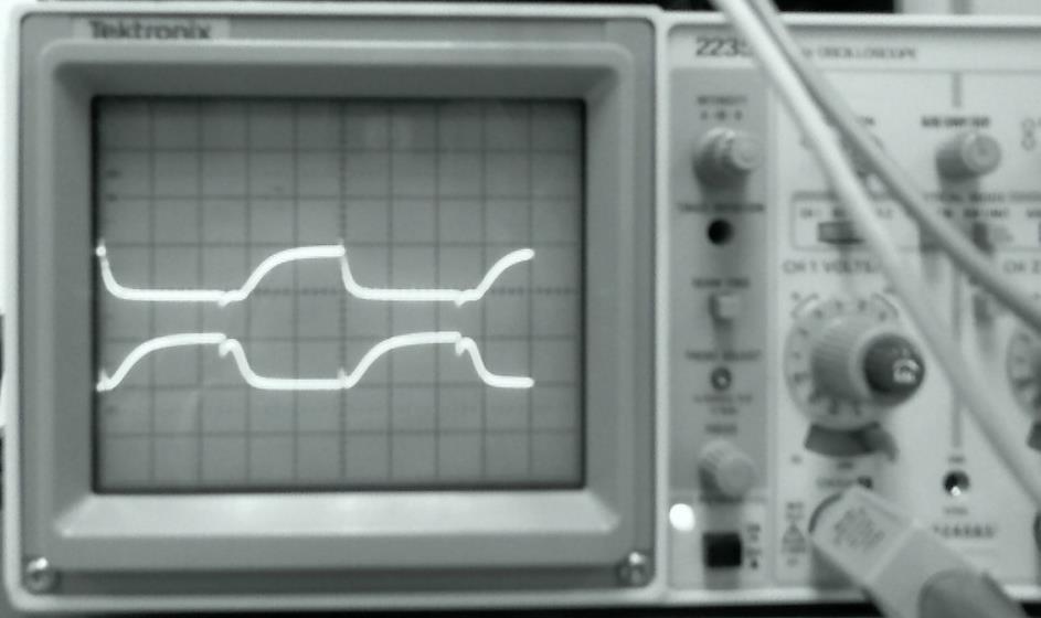
20 MEASURED RING OSCILLATOR OUTPUT RIT 2µm CMOS Ring Oscillator 73 Stage Ring at 5V td = 104.8ns / 2(73) = ns Rob Saxer 2005 Page 20


21 MOSFETS IN THE INVERTER OF 73 RING OSCILLATOR nmosfet pmosfet 73 Stage Ring Oscillator Page 21
22 FIND DIMENSIONS OF THE TRANSISTORS NMOS PMOS L 2u 2u W 12u 30u AD 12ux12u=144p 12ux30u=360p AS 12ux12u=144p 12ux30u=360p PD 2x(12u+12u)=48u 2x(12u+30u)=84u PS 2x(12u+12u)=48u 2x(12u+30u)=84u NRS NRD Stage Use Ctrl Click on all NMOS on OrCad Schematic Use Rochester Ctrl Institute Click of Technology on all PMOS on OrCad Schematic Then Enter Dimensions Page 22
23 SPICE MODELS FOR MOSFETS * LTSPICE uses Level=8 *For RIT Sub-CMOS 150 process with L=2u.MODEL RITSUBN8 NMOS (LEVEL=8 +VERSION=3.1 CAPMOD=2 MOBMOD=1 +TOX=1.5E-8 XJ=1.84E-7 NCH=1.45E17 NSUB=5.33E16 XT=8.66E-8 +VTH0=1.0 U0= 600 WINT=2.0E-7 LINT=1E-7 +NGATE=5E20 RSH=1082 JS=3.23E-8 JSW=3.23E-8 CJ=6.8E-4 MJ=0.5 PB=0.95 +CJSW=1.26E-10 MJSW=0.5 PBSW=0.95 PCLM=5 +CGSO=3.4E-10 CGDO=3.4E-10 CGBO=5.75E-10) * * LTSPICE uses Level=8 *For RIT Sub-CMOS 150 process with L=2u.MODEL RITSUBP8 PMOS (LEVEL=8 +VERSION=3.1 CAPMOD=2 MOBMOD=1 +TOX=1.5E-8 XJ=2.26E-7 NCH=7.12E16 NSUB=3.16E16 XT=8.66E-8 +VTH0=-1.0 U0= WINT=2.0E-7 LINT=2.26E-7 +NGATE=5E20 RSH=1347 JS=3.51E-8 JSW=3.51E-8 CJ=5.28E-4 MJ=0.5 PB=0.94 +CJSW=1.19E-10 MJSW=0.5 PBSW=0.94 +CGSO=4.5E-10 CGDO=4.5E-10 CGBO=5.75E-10) Page 23
24 FIND DIMENSIONS OF THE TRANSISTORS NMOS PMOS L 2u 2u W 12u 30u AD 12ux12u=144p 12ux30u=360p AS 12ux12u=144p 12ux30u=360p PD 2x(12u+12u)=48u 2x(12u+30u)=84u PS 2x(12u+12u)=48u 2x(12u+30u)=84u NRS NRD Stage Use Ctrl Click on all NMOS on OrCad Schematic Use Rochester Ctrl Institute Click of Technology on all PMOS on OrCad Schematic Then Enter Dimensions Page 24

25 GATE DELAY FROM SPICE Equal L and W Gate Rochester delay Institute is the of Technology time to get to 50% of the final value. td LTH = 441ns td HTL = 328ns Page 25
26 GATE DELAY Equal L and W Include parameters Gate Rochester delay Institute is of the Technology time to get to 50% of the final value. td LTH = 825ns td HTL = 599ns Page 26
27 INVERTER MODEL FOR LTH AND HTL TRANSISTION +V ReqP PMOS NMOS ReqN Ipmos Inmos Cin -125uA +100uA ReqN = ~ Vave/Iave = 3.75/125uA = 30K ohms ReqP = ~ Vave/Iave = 3.75/100uA = 38K ohms Gate delay is the time to get to 50% of the final value. Page 27
28 INVERTER RISE TIME AND FALL TIME ReqN = ~ Vave/Iave = 3.75/125uA = 30K ohms ReqP = ~ Vave/Iave = 3.75/100uA = 38K ohms RN = 1/(q µ n Dose) x Lnmos/Wnmos RP = 1/(q µ p Dose) x Lpmos/Wpmos Rise/Fall time is defined as the time for Vout to go from10% to 90%. For rise time equal to fall time the RC time constants are equal RN Cin = RP Cin Lnmos/(Wnmos µn) = Lpmos/(Wpmos µp) µp / µn = (Lpmos/Wpmos) / (Lnmos/Wnmos) Often Lpmos = Lnmos Finally µp / µn = (Wnmos/Wpmos) Wpmos = Wnmos (µn/µp) Page 28
29 Mobility (cm 2 / V sec) MOBILITY ^13 10^14 holes 10^15 10^16 electrons 10^17 10^18 Total Impurity Concentration (cm -3 ) See Dr. Fuller s Mobility Calculator 10^19 10^20 Electron Arsenic and hole mobilities in silicon Boron at 300 K as functions Phosphorus of the total dopant concentration (N). The values plotted are the results of the curve fitting measurements from several sources. The mobility curves can be generated using the equation below with the parameters shown: µ(n) = µ mi + (µ max-µ min ) {1 + (N/N ref ) } From Muller and Kamins, 3 rd Ed., pg 33 Parameter Arsenic Phosphorous Boron µ min µ max N ref 9.68X10^ X10^ X10^ Page 29
30 RISE TIME EQUALS FALL TIME Wpmos = 1.5 x Wnmos Gate Rochester delay Institute is of the Technology time to get to 50% of the final value. td LTH = 526ns td HTL = 663ns Page 30

31 RISE TIME EQUALS FALL TIME Wpmos = 1.25 x Wnmos Gate Rochester delay Institute is of the Technology time to get to 50% of the final value. td LTH = 604ns td HTL = 652ns Page 31
32 LOGIC GATE RISE TIME AND FALL TIME The inverter rise time is determined by the channel resistance and the capacitance to be charged or discharged. PMOS +V ReqP = 38K L/W Ipmos For L=1um and W=5um RC=34K/5 x 51.9fF = 0.353ns NMOS Inmos Cself Cwire CG ReqN= 30K L/W 26.6fF zeroff 25.3fF Page 32


33 WIRE RESISTANCE AND CAPACITANCE, LOW K, CU The wiring is typically aluminum or copper. The resistivity of aluminum is 26.5 nohm-cm and copper is 17.1 nohm-cm thus the wire will be lower resistance if copper. Page 33

34 MULTILAYER METAL, W PLUGS, CMP 8 Layers Metal Page 34


35 LOW-K FOR INTERCONNECT Page 35
36 LOGIC GATES RISE TIME AND FALL TIME The design guide line is that the logic gate under consideration should have the same rise time and fall time as the inverter (after we adjusted the inverter for equal rise time and fall time. Assume L s are the same. (W/L) pullup = ~ 1.5 (W/L) pulldown based on mobility only VA VB VOUT 3W +V VA VB NOR NAND W +V VA VB 1.5W VOUT W VA 3W NOR W VB VA 2W 2W NAND VB Page 36
37 SIZING AND TIMING FOR THREE-INPUT NAND To achieve equal rise time and fall time (and make these times approximately equal to the simple inverter rise time and fall time). The transistors length and width can be calculated. In the simple inverter the nmos W/L is the smallest values for that technology. The pmos is 1.5 times wider to give equal drive current. For a more complex gate there will be transistors in series and parallel and those combinations need to be considered when trying to achieve rise and fall times equivalent to the simple inverter. For example: M1, M2 and M3 have a combined length of 3L So the combined width should be 3W to give drive current equivalent to the nmos in the simple inverter. Each nmos 3W/L The pmos have a combined width of 3W and a length of L. The simple inverter calls for the pmos to have W/L of 1.5 so make L two times the L of the simple inverter. W/2L VA M2 M3 +V W/2L W/2L M1 3W/L 3W/L 3W/L VOUT VB VC Page 37
38 FAN IN AND FAN OUT CONSIDERATIONS Fan in refers to the number of inputs to a gate. It is common to have up to 8 inputs. In CMOS this implies that there are 8 transistors in parallel and 8 transistors in series. The 8 in parallel is not necessarily a problem but the 8 in series is because of the body effect on the threshold voltage of some of the transistors if they are all in the same well (at Vss or Vdd for p-well or n-well respectively) The solution to this problem is to use a Pseudo CMOS logic gate where the series transistors are replaced by a single transistor with the gate wired to VDD or Ground for NMOS or PMOS respectively. This transistor is always on. Fan-In = 6 Page 38

39 FAN IN AND FAN OUT CONSIDERATIONS What is the correct sizing for the transistors in this gate? Fan-In = 6 1.5W 2W Page 39
40 FAN OUT GATE CAPACITANCE Fan out refers to the number of gates connected to the output of a gate. Each gate adds more capacitance to be charged or discharged during switching which has implications on rise time, fall time and gate delay. The size (W and L) of the MOSFETS in the gate, G1, can be set to keep the gate delay small. C G = C Gin + C G-S + C G-D (1-Av) = 23fF + 2.3fF + 2.3fF x (1- -5) = ~25fF Fan-Out = 6 C fan-out = Fan-Out x (C G ) = 6 x 25fF = 150fF G1 C G C G C G C G C G C G Page 40
41 MONO STABLE MULTIVIBRATOR This circuit will give a pulse at Vout whose width depends on RC time constant. V DD = 5 V V trigger V DD 0 1 s R 1 2 V 2 3 C V F t V out 27 kω V C Start with Vtrigger=0 and Vc=0 Page 41
42 TWO PHASE NON OVERLAPPING CLOCK Synchronous circuits that use the two phase non overlapping clock can separate input quantities from output quantities used to calculate the results in feedback systems such as the finite state machine. 1 2 Page 42

43 SWITCHED CAPACITOR VOLTAGE DOUBLER 2 2 C1 1 Vdd C1 C Load R Load 2 Another example for two phase non overlapping clocks Page 43
44 TWO-PHASE CLOCK GENERATORS A B C CLOCK t 1 CLOCKBAR R S t 2 t 3 Q 1 2 R S Q 0 0 Qn INDETERMINATE CLOCK CLOCK BAR 1 t 1 t 2 t 1 2 t 3 t 3 = Page 44


45 TRANSISTOR LEVEL SCHEMATIC OF 2 PHASE CLOCK +V Layout 1 Clock 2 +V Page 45


46 TWO PHASE NON OVERLAPPING CLOCK Clock 1 2 Page 46

47 CMOS TWO PHASE NON-OVERLAPPING CLOCK Page 47
48 CMOS TWO PHASE NON-OVERLAPPING CLOCK Page 48

49 SIMULATION NON-OVERLAPPING CLOCK + BUFFERS CLOCK R t 2 1 t 1 BUFFERS CLOCKBAR S t 3 2 Page 49
50 SIMULATION NON-OVERLAPPING CLOCK + BUFFERS CLOCK R t 2 1 t 1 BUFFERS CLOCKBAR S t pF Loads Page 50

51 SIMULATION NON-OVERLAPPING CLOCK + BUFFERS CLOCK R t 2 1 t 1 BUFFERS CLOCKBAR S t 3 2 5pF Loads 10pF Loads Page 51

52 SIMULATION NON-OVERLAPPING CLOCK + BUFFERS CLOCK R t 2 1 t 1 BUFFERS CLOCKBAR S t 3 2 4xL 16xL Page 52
53 SIMULATION NON-OVERLAPPING CLOCK + BUFFERS CLOCK R t 2 1 t 1 BUFFERS CLOCKBAR S t pF Loads Page 53
 to other chips, other PCB s, and other devices.")
54 CMOS TRISTATE INPUT OUTPUT PAD The Input/Output/Tristate Pad is the interface between the chip and the rest of the system. The pad is typically connected via a printed circuit board (PCB) to other chips, other PCB s, and other devices. If an oscilloscope probe is connected to a chip it represents a large capacitive load (~10pF) in parallel with a 1MEG or 10MEG resistor. If the chip is connected in parallel with other chips (as is done in memory) via a data bus it represents a large capacitive load to the chip. In the case of a data bus the pad could be for an input or an output signal or high impedance (thus Tri State) Also, these pads are subject to possible electrostatic discharge (ESD) as connections are made to the pads. Page 54
55 TRISTATE I/O PAD WITH ESD PROTECTION - SCHEMATIC l/w=5/40 Vdd l/w=5/40 l/w=5/2000 l/w=5/20 Data Vdd l/w=5/20 Vdd Pad Vdd l/w=5/10 l/w=5/ l/w=5/46 Enable l/w=5/40 Vin l/w=5/20 l/w=5/20 l/w=5/20 l/w=5/1000 l/w=5/28 Page 55

56 TRISTATE I/O PAD WITH ESD PROTECTION - LAYOUT Page 56
 can generate high voltages.")
57 ELECTROSTATIC DISCHARGE Electrostatic Discharge (ESD) Dielectric Breakdown Strength of SiO2 is approximately 8 E6 V/cm, thus a 250 Å gate oxide will not sustain voltages in excess of 20 V Triboelectricity (electricity produced by rubbing two materials together) can generate high voltages. A person walking across a room can generate 20,000 Volts and if discharged into an IC can cause immediate failure or damage that will reduce operating life. Even with proper handling several hundred volts can be applied to the IC. Therefore, protection circuitry is needed to provide a safe path for discharge of this electricity. Page 57


58 ESD DAMAGE Page 58
59 ELECTROSTATIC DISCHARGE - PROTECTION CIRCUITRY VDD PAD R -10 I 0.7 V FIRST TRANSISTOR GATE Page 59
60 ELECTROSTATIC DISCHARGE - MODEL Human Model: 0 to 5000 Volts R = 1500 ohms L = 7.5 µh C = 100 pf R VDD Machine Model One: 0 to 100 Volts R = 100 ohms R VDD Machine Model Two L = 1.0 µh C = 200 pf R = 10 ohms Charged Device Model L = 50 nh C = 10 pf R = 1 ohms Page 60
61 REFERNCES 1. Hodges Jackson and Saleh, Analysis and Design of Digital Integrated Circuits, Chapter Sedra and Smith, Microelectronic Circuits, Sixth Edition, Chapter Dr. Fuller s Lecture Notes, Page 61
62 HOMEWORK HIGH SPEED LOGIC 1. Investigate a 100nm ring oscillator. Does the number of stages change the period of oscillation, explain. Does the number of stages change the inverter gate delay, td, explain. Does the size of the transistors affect the period of oscillation, explain. Does the supply voltage, VDD, affect the period of oscillation, explain. Does the temperature affect the period of oscillation, explain. 2. Use SPICE to illustrate some of the questions in problem The simple hand calculation for inverter gate delay, td, uses Resistors to represent the PMOS and NMOS transistors and capacitors to represent the gate self capacitance and input capacitance. Assume the wiring capacitance is zero. How are the resistors and capacitors different for 1um technology compared to 100nm technology. Provide approximate values for the resistors and capacitors for both technologies. Page 62
63 HOMEWORK HIGH SPEED LOGIC 4. Pro 4 5. Pro 5 6. Pro 6 Page 63
64 SPICE MODELS FOR MOSFETS *SPICE MODELS FOR RIT DEVICES - DR. LYNN FULLER *LOCATION DR.FULLER'S WEBPAGE - * *Used in Electronics II for CD4007 inverter chip *Note: Properties L=1u W=200u.MODEL RIT4007N7 NMOS (LEVEL=7 +VERSION=3.1 CAPMOD=2 MOBMOD=1 +TOX=1.5E-8 XJ=1.84E-7 NCH=1.45E17 NSUB=5.33E16 XT=8.66E-8 +VTH0=1.0 U0= 600 WINT=2.0E-7 LINT=1E-7 +NGATE=5E20 RSH=1082 JS=3.23E-8 JSW=3.23E-8 CJ=6.8E-4 MJ=0.5 PB=0.95 +CJSW=1.26E-10 MJSW=0.5 PBSW=0.95 PCLM=5 +CGSO=3.4E-10 CGDO=3.4E-10 CGBO=5.75E-10) * *Used in Electronics II for CD4007 inverter chip *Note: Properties L=1u W=200u.MODEL RIT4007P7 PMOS (LEVEL=7 +VERSION=3.1 CAPMOD=2 MOBMOD=1 +TOX=1.5E-8 XJ=2.26E-7 NCH=7.12E16 NSUB=3.16E16 XT=8.66E-8 +VTH0=-1.0 U0= WINT=2.0E-7 LINT=2.26E-7 +NGATE=5E20 RSH=1347 JS=3.51E-8 JSW=3.51E-8 CJ=5.28E-4 MJ=0.5 PB=0.94 +CJSW=1.19E-10 MJSW=0.5 PBSW=0.94 +CGSO=4.5E-10 CGDO=4.5E-10 CGBO=5.75E-10) Page 64
65 SPICE MODELS FOR MOSFETS *Used for ALD1103 chips *Note: Properties L=10u W=880u.MODEL RITALDN3 NMOS (LEVEL=3 +TPG=1 TOX=6.00E-8 LD=2.08E-6 WD=4.00E-7 +U0= 1215 VTO=0.73 THETA=0.222 RS=0.74 RD=0.74 DELTA=2.5 +NSUB=1.57E16 XJ=1.3E-6 VMAX=4.38E6 ETA=0.913 KAPPA=0.074 NFS=3E11 +CGSO=5.99E-10 CGDO=5.99E-10 CGBO=4.31E-10 PB=0.90 XQC=0.4) * *Used for ALD1103 chips *Note: Properties L=10u W=880u.MODEL RITALDP3 PMOS (LEVEL=3 +TPG=1 TOX=6.00E-8 LD=2.08E-6 WD=4.00E-7 +U0=550 VTO=-0.73 THETA=0.222 RS=0.74 RD=0.74 DELTA=2.5 +NSUB=1.57E16 XJ=1.3E-6 VMAX=4.38E6 ETA=0.913 KAPPA=0.074 NFS=3E11 +CGSO=5.99E-10 CGDO=5.99E-10 CGBO=4.31E-10 PB=0.90 XQC=0.4) Page 65
66 SPICE MODELS FOR MOSFETS * LTSPICE uses Level=8 *For RIT Sub-CMOS 150 process with L=2u.MODEL RITSUBN8 NMOS (LEVEL=8 +VERSION=3.1 CAPMOD=2 MOBMOD=1 +TOX=1.5E-8 XJ=1.84E-7 NCH=1.45E17 NSUB=5.33E16 XT=8.66E-8 +VTH0=1.0 U0= 600 WINT=2.0E-7 LINT=1E-7 +NGATE=5E20 RSH=1082 JS=3.23E-8 JSW=3.23E-8 CJ=6.8E-4 MJ=0.5 PB=0.95 +CJSW=1.26E-10 MJSW=0.5 PBSW=0.95 PCLM=5 +CGSO=3.4E-10 CGDO=3.4E-10 CGBO=5.75E-10) * * LTSPICE uses Level=8 *For RIT Sub-CMOS 150 process with L=2u.MODEL RITSUBP8 PMOS (LEVEL=8 +VERSION=3.1 CAPMOD=2 MOBMOD=1 +TOX=1.5E-8 XJ=2.26E-7 NCH=7.12E16 NSUB=3.16E16 XT=8.66E-8 +VTH0=-1.0 U0= WINT=2.0E-7 LINT=2.26E-7 +NGATE=5E20 RSH=1347 JS=3.51E-8 JSW=3.51E-8 CJ=5.28E-4 MJ=0.5 PB=0.94 +CJSW=1.19E-10 MJSW=0.5 PBSW=0.94 +CGSO=4.5E-10 CGDO=4.5E-10 CGBO=5.75E-10) Page 66
67 SPICE MODELS FOR MOSFETS * From Sub-Micron CMOS Manufacturing Classes in MicroE ~ 1um Technology.MODEL RITSUBN7 NMOS (LEVEL=7 +VERSION=3.1 CAPMOD=2 MOBMOD=1 +TOX=1.5E-8 XJ=1.84E-7 NCH=1.45E17 NSUB=5.33E16 XT=8.66E-8 +VTH0=1.0 U0= 600 WINT=2.0E-7 LINT=1E-7 +NGATE=5E20 RSH=1082 JS=3.23E-8 JSW=3.23E-8 CJ=6.8E-4 MJ=0.5 PB=0.95 +CJSW=1.26E-10 MJSW=0.5 PBSW=0.95 PCLM=5 +CGSO=3.4E-10 CGDO=3.4E-10 CGBO=5.75E-10) * *From Sub-Micron CMOS Manufacturing Classes in MicroE ~ 1um Technology.MODEL RITSUBP7 PMOS (LEVEL=7 +VERSION=3.1 CAPMOD=2 MOBMOD=1 +TOX=1.5E-8 XJ=2.26E-7 NCH=7.12E16 NSUB=3.16E16 XT=8.66E-8 +VTH0=-1.0 U0= WINT=2.0E-7 LINT=2.26E-7 +NGATE=5E20 RSH=1347 JS=3.51E-8 JSW=3.51E-8 CJ=5.28E-4 MJ=0.5 PB=0.94 +CJSW=1.19E-10 MJSW=0.5 PBSW=0.94 +CGSO=4.5E-10 CGDO=4.5E-10 CGBO=5.75E-10) Page 67
68 SPICE MODELS FOR MOSFETS * LTSPICE uses Level=8 * From Electronics II EEEE482 FOR ~100nm Technology.model EECMOSN NMOS (LEVEL=8 +VERSION=3.1 CAPMOD=2 MOBMOD=1 +TOX=5E-9 XJ=1.84E-7 NCH=1E17 NSUB=5E16 XT=5E-8 +VTH0=0.4 U0= 200 WINT=1E-8 LINT=1E-8 +NGATE=5E20 RSH=1000 JS=3.23E-8 JSW=3.23E-8 CJ=6.8E-4 MJ=0.5 PB=0.95 +CJSW=1.26E-10 MJSW=0.5 PBSW=0.95 PCLM=5 +CGSO=3.4E-10 CGDO=3.4E-10 CGBO=5.75E-10) * * LTSPICE uses Level=8 * From Electronics II EEEE482 FOR ~100nm Technology.model EECMOSP PMOS (LEVEL=8 +TOX=5E-9 XJ=0.05E-6 NCH=1E17 NSUB=5E16 XT=5E-8 +VTH0=-0.4 U0= 100 WINT=1E-8 LINT=1E-8 +NGATE=5E20 RSH=1000 JS=3.51E-8 JSW=3.51E-8 CJ=5.28E-4 MJ=0.5 PB=0.94 +CJSW=1.19E-10 MJSW=0.5 PBSW=0.94 PCLM=5 +CGSO=4.5E-10 CGDO=4.5E-10 CGBO=5.75E-10) * Page 68
MOSFET Internal Capacitance Dr. Lynn Fuller Webpage:
 ROCHESTER INSTITUTE OF TECHNOLOGY MICROELECTRONIC ENGINEERING Dr. Lynn Fuller Webpage: http://people.rit.edu/lffeee 82 Lomb Memorial Drive Rochester, NY 14623-5604 Email: Lynn.Fuller@rit.edu Department
Combinatorial and Sequential CMOS Circuits Dr. Lynn Fuller Webpage:
 ROCHESTER INSTITUTE OF TECHNOLOGY MICROELECTRONIC ENGINEERING Combinatorial and Sequential CMOS Circuits Webpage: http://people.rit.edu/lffeee 82 Lomb Memorial Drive Rochester, NY 14623-5604 Tel (585)
Transfer Gate and Dynamic Logic Dr. Lynn Fuller Webpage:
 ROCHESTER INSTITUTE OF TECHNOLOGY MICROELECTRONIC ENGINEERING Transfer Gate and Dynamic Logic Dr. Lynn Fuller Webpage: http://people.rit.edu/lffeee 82 Lomb Memorial Drive Rochester, NY 14623-5604 Tel (585)
MOS Amplifiers Dr. Lynn Fuller Webpage:
 ROCHESTER INSTITUTE OF TECHNOLOGY MICROELECTRONIC ENGINEERING Dr. Lynn Fuller Webpage: http://people.rit.edu/lffeee 82 Lomb Memorial Drive Rochester, NY 14623-5604 Email: Lynn.Fuller@rit.edu Department
Low Power CMOS Dr. Lynn Fuller Webpage:
 ROCHESTER INSTITUTE OF TECHNOLOGY MICROELECTRONIC ENGINEERING Dr. Lynn Fuller Webpage: http://people.rit.edu/lffeee 82 Lomb Memorial Drive Rochester, NY 14623-5604 Email: Lynn.Fuller@rit.edu Department
ESE 570: Digital Integrated Circuits and VLSI Fundamentals
 ESE 570: Digital Integrated Circuits and VLSI Fundamentals Lec 6: January 30, 2018 MOS Operating Regions, pt. 2 Lecture Outline! Operating Regions (review) " Subthreshold " Resistive " Saturation! Intro.
The Devices. Devices
 The The MOS Transistor Gate Oxyde Gate Source n+ Polysilicon Drain n+ Field-Oxyde (SiO 2 ) p-substrate p+ stopper Bulk Contact CROSS-SECTION of NMOS Transistor Cross-Section of CMOS Technology MOS transistors
ESE 570 MOS TRANSISTOR THEORY Part 2
 ESE 570 MOS TRANSISTOR THEORY Part 2 GCA (gradual channel approximation) MOS Transistor Model Strong Inversion Operation CMOS = NMOS + PMOS 2 TwoTerminal MOS Capacitor > nmos Transistor VGS
! MOS Capacitances. " Extrinsic. " Intrinsic. ! Lumped Capacitance Model. ! First Order Capacitor Summary. ! Capacitance Implications
 ESE 570: Digital Integrated Circuits and VLSI Fundamentals Lec 7: February, 07 MOS SPICE Models, MOS Parasitic Details Lecture Outline! MOS Capacitances " Extrinsic " Intrinsic! Lumped Capacitance Model!
ECE 546 Lecture 10 MOS Transistors
 ECE 546 Lecture 10 MOS Transistors Spring 2018 Jose E. Schutt-Aine Electrical & Computer Engineering University of Illinois jesa@illinois.edu NMOS Transistor NMOS Transistor N-Channel MOSFET Built on p-type
ESE 570: Digital Integrated Circuits and VLSI Fundamentals
 ESE 570: Digital Integrated Circuits and VLSI Fundamentals Lec 7: February 4, 2016 MOS SPICE Models, MOS Parasitic Details Lecture Outline! MOS Capacitances " Extrinsic " Intrinsic! Lumped Capacitance
ENEE 359a Digital VLSI Design
 SLIDE 1 ENEE 359a Digital VLSI Design & Logical Effort Prof. blj@ece.umd.edu Credit where credit is due: Slides contain original artwork ( Jacob 2004) as well as material taken liberally from Irwin & Vijay
ECE 342 Electronic Circuits. 3. MOS Transistors
 ECE 342 Electronic Circuits 3. MOS Transistors Jose E. Schutt-Aine Electrical & Computer Engineering University of Illinois jschutt@emlab.uiuc.edu 1 NMOS Transistor Typically L = 0.1 to 3 m, W = 0.2 to
(S&S ) PMOS: holes flow from Source to Drain. from Source to Drain. W.-Y. Choi. Electronic Circuits 2 (09/1)
 PMOS: holes flow from Source to Drain. from Source to Drain. W.-Y. Choi. Electronic Circuits 2 (09/1)") (S&S 4.1 4.3) NMOS: electrons flow from Source to Drain PMOS: holes flow from Source to Drain In cut-off ( v < V ), i = 0 GS t D NMOS I-V Characteristics In triode, ( v > V but v v v ) GS t DS GS T W 1
(S&S 4.1 4.3) NMOS: electrons flow from Source to Drain PMOS: holes flow from Source to Drain In cut-off ( v < V ), i = 0 GS t D NMOS I-V Characteristics In triode, ( v > V but v v v ) GS t DS GS T W 1
EE 330 Homework 5 Spring 2017 (This assignment will not be collected or graded)
") EE 330 Homework 5 Spring 2017 (This assignment will not be collected or graded) Assume the CMOS process is characterized by model parameters V TH =1V and µc OX =100µA/V 2. If any other model parameters
EE 330 Homework 5 Spring 2017 (This assignment will not be collected or graded) Assume the CMOS process is characterized by model parameters V TH =1V and µc OX =100µA/V 2. If any other model parameters
Fig. 1 CMOS Transistor Circuits (a) Inverter Out = NOT In, (b) NOR-gate C = NOT (A or B)
 Inverter Out = NOT In, (b) NOR-gate C = NOT (A or B)") 1 Introduction to Transistor-Level Logic Circuits 1 By Prawat Nagvajara At the transistor level of logic circuits, transistors operate as switches with the logic variables controlling the open or closed
1 Introduction to Transistor-Level Logic Circuits 1 By Prawat Nagvajara At the transistor level of logic circuits, transistors operate as switches with the logic variables controlling the open or closed
VLSI GATE LEVEL DESIGN UNIT - III P.VIDYA SAGAR ( ASSOCIATE PROFESSOR) Department of Electronics and Communication Engineering, VBIT
 Department of Electronics and Communication Engineering, VBIT") VLSI UNIT - III GATE LEVEL DESIGN P.VIDYA SAGAR ( ASSOCIATE PROFESSOR) contents GATE LEVEL DESIGN : Logic Gates and Other complex gates, Switch logic, Alternate gate circuits, Time Delays, Driving large
VLSI UNIT - III GATE LEVEL DESIGN P.VIDYA SAGAR ( ASSOCIATE PROFESSOR) contents GATE LEVEL DESIGN : Logic Gates and Other complex gates, Switch logic, Alternate gate circuits, Time Delays, Driving large
CMPEN 411 VLSI Digital Circuits. Lecture 03: MOS Transistor
 CMPEN 411 VLSI Digital Circuits Lecture 03: MOS Transistor Kyusun Choi [Adapted from Rabaey s Digital Integrated Circuits, Second Edition, 2003 J. Rabaey, A. Chandrakasan, B. Nikolic] CMPEN 411 L03 S.1
Study of MOSFET circuit
 ECE 570 Computer Aided Engineering for Integrated Circuits IC 752 - E Simulation Assignment No. 3 - Due: Oct. 30 (Th.), 2003 Study of MOSFET circuit Simulate the basic circuit of CMOS shift register shown
Topics to be Covered. capacitance inductance transmission lines
 Topics to be Covered Circuit Elements Switching Characteristics Power Dissipation Conductor Sizes Charge Sharing Design Margins Yield resistance capacitance inductance transmission lines Resistance of
Lecture 0: Introduction
 Lecture 0: Introduction Introduction q Integrated circuits: many transistors on one chip q Very Large Scale Integration (VLSI): bucketloads! q Complementary Metal Oxide Semiconductor Fast, cheap, low power
The Physical Structure (NMOS)
") The Physical Structure (NMOS) Al SiO2 Field Oxide Gate oxide S n+ Polysilicon Gate Al SiO2 SiO2 D n+ L channel P Substrate Field Oxide contact Metal (S) n+ (G) L W n+ (D) Poly 1 Transistor Resistance Two
The Physical Structure (NMOS) Al SiO2 Field Oxide Gate oxide S n+ Polysilicon Gate Al SiO2 SiO2 D n+ L channel P Substrate Field Oxide contact Metal (S) n+ (G) L W n+ (D) Poly 1 Transistor Resistance Two
MOSFET: Introduction
 E&CE 437 Integrated VLSI Systems MOS Transistor 1 of 30 MOSFET: Introduction Metal oxide semiconductor field effect transistor (MOSFET) or MOS is widely used for implementing digital designs Its major
Very Large Scale Integration (VLSI)
") Very Large Scale Integration (VLSI) Lecture 4 Dr. Ahmed H. Madian Ah_madian@hotmail.com Dr. Ahmed H. Madian-VLSI Contents Delay estimation Simple RC model Penfield-Rubenstein Model Logical effort Delay
Very Large Scale Integration (VLSI) Lecture 4 Dr. Ahmed H. Madian Ah_madian@hotmail.com Dr. Ahmed H. Madian-VLSI Contents Delay estimation Simple RC model Penfield-Rubenstein Model Logical effort Delay
S No. Questions Bloom s Taxonomy Level UNIT-I
 GROUP-A (SHORT ANSWER QUESTIONS) S No. Questions Bloom s UNIT-I 1 Define oxidation & Classify different types of oxidation Remember 1 2 Explain about Ion implantation Understand 1 3 Describe lithography
Lecture 4: CMOS Transistor Theory
 Introduction to CMOS VLSI Design Lecture 4: CMOS Transistor Theory David Harris, Harvey Mudd College Kartik Mohanram and Steven Levitan University of Pittsburgh Outline q Introduction q MOS Capacitor q
University of Pennsylvania Department of Electrical Engineering. ESE 570 Midterm Exam March 14, 2013 FORMULAS AND DATA
 University of Pennsylvania Department of Electrical Engineering ESE 570 Midterm Exam March 4, 03 FORMULAS AND DATA. PHYSICAL CONSTANTS: n i = intrinsic concentration undoped) silicon =.45 x 0 0 cm -3 @
L ECE 4211 UConn F. Jain Scaling Laws for NanoFETs Chapter 10 Logic Gate Scaling
 L13 04202017 ECE 4211 UConn F. Jain Scaling Laws for NanoFETs Chapter 10 Logic Gate Scaling Scaling laws: Generalized scaling (GS) p. 610 Design steps p.613 Nanotransistor issues (page 626) Degradation
EE 330 Homework 5 Fall 2018 (This assignment is due Wednesday Sept 19 at 12:00 noon)
") EE 330 Homework 5 Fall 2018 (This assignment is due Wednesday Sept 19 at 12:00 noon) Assume the CMOS process is characterized by model parameters VTH=1V and µcox=100µa/v 2. If any other model parameters
EE 330 Homework 5 Fall 2018 (This assignment is due Wednesday Sept 19 at 12:00 noon) Assume the CMOS process is characterized by model parameters VTH=1V and µcox=100µa/v 2. If any other model parameters
P. R. Nelson 1 ECE418 - VLSI. Midterm Exam. Solutions
 P. R. Nelson 1 ECE418 - VLSI Midterm Exam Solutions 1. (8 points) Draw the cross-section view for A-A. The cross-section view is as shown below.. ( points) Can you tell which of the metal1 regions is the
CMOS Inverter (static view)
") Review: Design Abstraction Levels SYSTEM CMOS Inverter (static view) + MODULE GATE [Adapted from Chapter 5. 5.3 CIRCUIT of G DEVICE Rabaey s Digital Integrated Circuits,, J. Rabaey et al.] S D Review:
Review: Design Abstraction Levels SYSTEM CMOS Inverter (static view) + MODULE GATE [Adapted from Chapter 5. 5.3 CIRCUIT of G DEVICE Rabaey s Digital Integrated Circuits,, J. Rabaey et al.] S D Review:
CMPEN 411 VLSI Digital Circuits. Lecture 04: CMOS Inverter (static view)
") CMPEN 411 VLSI Digital Circuits Lecture 04: CMOS Inverter (static view) Kyusun Choi [Adapted from Rabaey s Digital Integrated Circuits, Second Edition, 2003 J. Rabaey, A. Chandrakasan, B. Nikolic] CMPEN
CMPEN 411 VLSI Digital Circuits Lecture 04: CMOS Inverter (static view) Kyusun Choi [Adapted from Rabaey s Digital Integrated Circuits, Second Edition, 2003 J. Rabaey, A. Chandrakasan, B. Nikolic] CMPEN
Low Power VLSI Circuits and Systems Prof. Ajit Pal Department of Computer Science and Engineering Indian Institute of Technology, Kharagpur
 Low Power VLSI Circuits and Systems Prof. Ajit Pal Department of Computer Science and Engineering Indian Institute of Technology, Kharagpur Lecture No. # 08 MOS Inverters - III Hello, and welcome to today
ESE 570: Digital Integrated Circuits and VLSI Fundamentals
 ESE 570: Digital Integrated Circuits and VLSI Fundamentals Lec 4: January 23, 2018 MOS Transistor Theory, MOS Model Penn ESE 570 Spring 2018 Khanna Lecture Outline! CMOS Process Enhancements! Semiconductor
University of Toronto. Final Exam
 University of Toronto Final Exam Date - Apr 18, 011 Duration:.5 hrs ECE334 Digital Electronics Lecturer - D. Johns ANSWER QUESTIONS ON THESE SHEETS USING BACKS IF NECESSARY 1. Equation sheet is on last
Chapter 4 Field-Effect Transistors
 Chapter 4 Field-Effect Transistors Microelectronic Circuit Design Richard C. Jaeger Travis N. Blalock 5/5/11 Chap 4-1 Chapter Goals Describe operation of MOSFETs. Define FET characteristics in operation
EE115C Winter 2017 Digital Electronic Circuits. Lecture 3: MOS RC Model, CMOS Manufacturing
 EE115C Winter 2017 Digital Electronic Circuits Lecture 3: MOS RC Model, CMOS Manufacturing Agenda MOS Transistor: RC Model (pp. 104-113) S R on D CMOS Manufacturing Process (pp. 36-46) S S C GS G G C GD
The Intrinsic Silicon
 The Intrinsic ilicon Thermally generated electrons and holes Carrier concentration p i =n i ni=1.45x10 10 cm-3 @ room temp Generally: n i = 3.1X10 16 T 3/2 e -1.21/2KT cm -3 T= temperature in K o (egrees
APPENDIX D: Binning BSIM3v3 Parameters
 APPENDIX D: Binning BSIM3v3 Parameters Below is a list of all BSIM3v3 model parameters which can or cannot be binned. All model parameters which can be binned follow the following implementation: P L P
Integrated Circuit Design: OTA in 0.5µm Technology
 Integrated Circuit Design: OTA in 0.5µm Technology Omar X. Avelar, Omar de la Mora & Diego I. Romero INTEGRATED CIRCUITS DESIGN (ESI108A) Instituto Tecnológico y de Estudios Superiores de Occidente (ITESO)
Circuits. L2: MOS Models-2 (1 st Aug. 2013) B. Mazhari Dept. of EE, IIT Kanpur. B. Mazhari, IITK. G-Number
 B. Mazhari Dept. of EE, IIT Kanpur. B. Mazhari, IITK. G-Number") EE610: CMOS Analog Circuits L: MOS Models- (1 st Aug. 013) B. Mazhari Dept. of EE, IIT Kanpur 3 NMOS Models MOS MODEL Above Threshold Subthreshold ( GS > TN ) ( GS < TN ) Saturation ti Ti Triode ( DS >
EE610: CMOS Analog Circuits L: MOS Models- (1 st Aug. 013) B. Mazhari Dept. of EE, IIT Kanpur 3 NMOS Models MOS MODEL Above Threshold Subthreshold ( GS > TN ) ( GS < TN ) Saturation ti Ti Triode ( DS >
EE141Microelettronica. CMOS Logic
 Microelettronica CMOS Logic CMOS logic Power consumption in CMOS logic gates Where Does Power Go in CMOS? Dynamic Power Consumption Charging and Discharging Capacitors Short Circuit Currents Short Circuit
EEC 118 Lecture #2: MOSFET Structure and Basic Operation. Rajeevan Amirtharajah University of California, Davis Jeff Parkhurst Intel Corporation
 EEC 118 Lecture #2: MOSFET Structure and Basic Operation Rajeevan Amirtharajah University of California, Davis Jeff Parkhurst Intel Corporation Announcements Lab 1 this week, report due next week Bring
ESE 570: Digital Integrated Circuits and VLSI Fundamentals
 ESE 570: Digital Integrated Circuits and VLSI Fundamentals Lec 4: January 29, 2019 MOS Transistor Theory, MOS Model Penn ESE 570 Spring 2019 Khanna Lecture Outline! CMOS Process Enhancements! Semiconductor
APPENDIX A: Parameter List
 APPENDIX A: Parameter List A.1 BSIM3v3 Model Control Parameters none level BSIMv3 model selector 8 none Mobmod mobmod Mobility model selector 1 none Capmod capmod Flag for the short channel 1 none capacitance
MOS Transistor Theory
 CHAPTER 3 MOS Transistor Theory Outline 2 1. Introduction 2. Ideal I-V Characteristics 3. Nonideal I-V Effects 4. C-V Characteristics 5. DC Transfer Characteristics 6. Switch-level RC Delay Models MOS
APPENDIX A: Parameter List
 APPENDIX A: Parameter List A.1 BSIM3v3 Model Control Parameters none level BSIMv3 model selector 8 none Mobmod mobmod Mobility model selector 1 none Capmod capmod Flag for the short channel 2 none capacitance
Lecture 7 Circuit Delay, Area and Power
 Lecture 7 Circuit Delay, Area and Power lecture notes from S. Mitra Intro VLSI System course (EE271) Introduction to VLSI Systems 1 Circuits and Delay Introduction to VLSI Systems 2 Power, Delay and Area:
and V DS V GS V T (the saturation region) I DS = k 2 (V GS V T )2 (1+ V DS )
 I DS = k 2 (V GS V T )2 (1+ V DS )") ECE 4420 Spring 2005 Page 1 FINAL EXAMINATION NAME SCORE /100 Problem 1O 2 3 4 5 6 7 Sum Points INSTRUCTIONS: This exam is closed book. You are permitted four sheets of notes (three of which are your sheets
ECE 4420 Spring 2005 Page 1 FINAL EXAMINATION NAME SCORE /100 Problem 1O 2 3 4 5 6 7 Sum Points INSTRUCTIONS: This exam is closed book. You are permitted four sheets of notes (three of which are your sheets
ECE 342 Electronic Circuits. Lecture 6 MOS Transistors
 ECE 342 Electronic Circuits Lecture 6 MOS Transistors Jose E. Schutt-Aine Electrical & Computer Engineering University of Illinois jesa@illinois.edu 1 NMOS Transistor Typically L = 0.1 to 3 m, W = 0.2
ENGR890 Digital VLSI Design Fall Lecture 4: CMOS Inverter (static view)
") ENGR89 Digital VLSI Design Fall 5 Lecture 4: CMOS Inverter (static view) [Adapted from Chapter 5 of Digital Integrated Circuits, 3, J. Rabaey et al.] [Also borrowed from Vijay Narayanan and Mary Jane Irwin]
ENGR89 Digital VLSI Design Fall 5 Lecture 4: CMOS Inverter (static view) [Adapted from Chapter 5 of Digital Integrated Circuits, 3, J. Rabaey et al.] [Also borrowed from Vijay Narayanan and Mary Jane Irwin]
EEC 116 Lecture #5: CMOS Logic. Rajeevan Amirtharajah Bevan Baas University of California, Davis Jeff Parkhurst Intel Corporation
 EEC 116 Lecture #5: CMOS Logic Rajeevan mirtharajah Bevan Baas University of California, Davis Jeff Parkhurst Intel Corporation nnouncements Quiz 1 today! Lab 2 reports due this week Lab 3 this week HW
LECTURE 3 MOSFETS II. MOS SCALING What is Scaling?
 LECTURE 3 MOSFETS II Lecture 3 Goals* * Understand constant field and constant voltage scaling and their effects. Understand small geometry effects for MOS transistors and their implications modeling and
EEC 116 Lecture #3: CMOS Inverters MOS Scaling. Rajeevan Amirtharajah University of California, Davis Jeff Parkhurst Intel Corporation
 EEC 116 Lecture #3: CMOS Inverters MOS Scaling Rajeevan Amirtharajah University of California, Davis Jeff Parhurst Intel Corporation Outline Review: Inverter Transfer Characteristics Lecture 3: Noise Margins,
Practice 7: CMOS Capacitance
 Practice 7: CMOS Capacitance Digital Electronic Circuits Semester A 2012 MOSFET Capacitances MOSFET Capacitance Components 3 Gate to Channel Capacitance In general, the gate capacitance is similar to a
2007 Fall: Electronic Circuits 2 CHAPTER 10. Deog-Kyoon Jeong School of Electrical Engineering
 007 Fall: Electronic Circuits CHAPTER 10 Digital CMOS Logic Circuits Deog-Kyoon Jeong dkjeong@snu.ac.kr k School of Electrical Engineering Seoul lnational luniversity it Introduction In this chapter, we
6.012 Electronic Devices and Circuits
 Page 1 of 12 YOUR NAME Department of Electrical Engineering and Computer Science Massachusetts Institute of Technology 6.012 Electronic Devices and Circuits FINAL EXAMINATION Open book. Notes: 1. Unless
Lecture 3: CMOS Transistor Theory
 Lecture 3: CMOS Transistor Theory Outline Introduction MOS Capacitor nmos I-V Characteristics pmos I-V Characteristics Gate and Diffusion Capacitance 2 Introduction So far, we have treated transistors
Objective and Outline. Acknowledgement. Objective: Power Components. Outline: 1) Acknowledgements. Section 4: Power Components
 Acknowledgements. Section 4: Power Components") Objective: Power Components Outline: 1) Acknowledgements 2) Objective and Outline 1 Acknowledgement This lecture note has been obtained from similar courses all over the world. I wish to thank all the
Objective: Power Components Outline: 1) Acknowledgements 2) Objective and Outline 1 Acknowledgement This lecture note has been obtained from similar courses all over the world. I wish to thank all the
Lecture 5: DC & Transient Response
 Lecture 5: DC & Transient Response Outline q Pass Transistors q DC Response q Logic Levels and Noise Margins q Transient Response q RC Delay Models q Delay Estimation 2 Activity 1) If the width of a transistor
Lecture 12 CMOS Delay & Transient Response
 EE 471: Transport Phenomena in Solid State Devices Spring 2018 Lecture 12 CMOS Delay & Transient Response Bryan Ackland Department of Electrical and Computer Engineering Stevens Institute of Technology
Microelectronics Part 1: Main CMOS circuits design rules
 GBM8320 Dispositifs Médicaux telligents Microelectronics Part 1: Main CMOS circuits design rules Mohamad Sawan et al. Laboratoire de neurotechnologies Polystim! http://www.cours.polymtl.ca/gbm8320/! med-amine.miled@polymtl.ca!
UNIVERSITY OF CALIFORNIA College of Engineering Department of Electrical Engineering and Computer Sciences. Professor Oldham Fall 1999
 UNIVERSITY OF CLIFORNI College of Engineering Department of Electrical Engineering and Computer Sciences Professor Oldham Fall 1999 EECS 40 FINL EXM 13 December 1999 Name: Last, First Student ID: T: Kusuma
Digital Integrated Circuits EECS 312
 14 12 10 8 6 Fujitsu VP2000 IBM 3090S Pulsar 4 IBM 3090 IBM RY6 CDC Cyber 205 IBM 4381 IBM RY4 2 IBM 3081 Apache Fujitsu M380 IBM 370 Merced IBM 360 IBM 3033 Vacuum Pentium II(DSIP) 0 1950 1960 1970 1980
MOS Transistor I-V Characteristics and Parasitics
 ECEN454 Digital Integrated Circuit Design MOS Transistor I-V Characteristics and Parasitics ECEN 454 Facts about Transistors So far, we have treated transistors as ideal switches An ON transistor passes
VLSI VLSI CIRCUIT DESIGN PROCESSES P.VIDYA SAGAR ( ASSOCIATE PROFESSOR) Department of Electronics and Communication Engineering, VBIT
 Department of Electronics and Communication Engineering, VBIT") VLSI VLSI CIRCUIT DESIGN PROCESSES P.VIDYA SAGAR ( ASSOCIATE PROFESSOR) SYLLABUS UNIT II VLSI CIRCUIT DESIGN PROCESSES: VLSI Design Flow, MOS Layers, Stick Diagrams, Design Rules and Layout, 2 m CMOS Design
VLSI VLSI CIRCUIT DESIGN PROCESSES P.VIDYA SAGAR ( ASSOCIATE PROFESSOR) SYLLABUS UNIT II VLSI CIRCUIT DESIGN PROCESSES: VLSI Design Flow, MOS Layers, Stick Diagrams, Design Rules and Layout, 2 m CMOS Design
Device Models (PN Diode, MOSFET )
") Device Models (PN Diode, MOSFET ) Instructor: Steven P. Levitan steve@ece.pitt.edu TA: Gayatri Mehta, José Martínez Book: Digital Integrated Circuits: A Design Perspective; Jan Rabaey Lab Notes: Handed
Device Models (PN Diode, MOSFET ) Instructor: Steven P. Levitan steve@ece.pitt.edu TA: Gayatri Mehta, José Martínez Book: Digital Integrated Circuits: A Design Perspective; Jan Rabaey Lab Notes: Handed
6.012 Electronic Devices and Circuits Spring 2005
 6.012 Electronic Devices and Circuits Spring 2005 May 16, 2005 Final Exam (200 points) -OPEN BOOK- Problem NAME RECITATION TIME 1 2 3 4 5 Total General guidelines (please read carefully before starting):
The Devices: MOS Transistors
 The Devices: MOS Transistors References: Semiconductor Device Fundamentals, R. F. Pierret, Addison-Wesley Digital Integrated Circuits: A Design Perspective, J. Rabaey et.al. Prentice Hall NMOS Transistor
CARNEGIE MELLON UNIVERSITY DEPARTMENT OF ELECTRICAL AND COMPUTER ENGINEERING DIGITAL INTEGRATED CIRCUITS FALL 2002
 CARNEGIE MELLON UNIVERSITY DEPARTMENT OF ELECTRICAL AND COMPUTER ENGINEERING 18-322 DIGITAL INTEGRATED CIRCUITS FALL 2002 Final Examination, Monday Dec. 16, 2002 NAME: SECTION: Time: 180 minutes Closed
CMOS Transistors, Gates, and Wires
 CMOS Transistors, Gates, and Wires Should the hardware abstraction layers make today s lecture irrelevant? pplication R P C W / R W C W / 6.375 Complex Digital Systems Christopher atten February 5, 006
ELEN0037 Microelectronic IC Design. Prof. Dr. Michael Kraft
 ELEN0037 Microelectronic IC Design Prof. Dr. Michael Kraft Lecture 2: Technological Aspects Technology Passive components Active components CMOS Process Basic Layout Scaling CMOS Technology Integrated
Spiral 2 7. Capacitance, Delay and Sizing. Mark Redekopp
 2-7.1 Spiral 2 7 Capacitance, Delay and Sizing Mark Redekopp 2-7.2 Learning Outcomes I understand the sources of capacitance in CMOS circuits I understand how delay scales with resistance, capacitance
ECE 497 JS Lecture - 12 Device Technologies
 ECE 497 JS Lecture - 12 Device Technologies Spring 2004 Jose E. Schutt-Aine Electrical & Computer Engineering University of Illinois jose@emlab.uiuc.edu 1 NMOS Transistor 2 ρ Source channel charge density
Dynamic operation 20
 Dynamic operation 20 A simple model for the propagation delay Symmetric inverter (rise and fall delays are identical) otal capacitance is linear t p Minimum length devices R W C L t = 0.69R C = p W L 0.69
Today s lecture. EE141- Spring 2003 Lecture 4. Design Rules CMOS Inverter MOS Transistor Model
 - Spring 003 Lecture 4 Design Rules CMOS Inverter MOS Transistor Model Today s lecture Design Rules The CMOS inverter at a glance An MOS transistor model for manual analysis Important! Labs start next
Lecture 04 Review of MOSFET
 ECE 541/ME 541 Microelectronic Fabrication Techniques Lecture 04 Review of MOSFET Zheng Yang (ERF 3017, email: yangzhen@uic.edu) What is a Transistor? A Switch! An MOS Transistor V GS V T V GS S Ron D
Integrated Circuits & Systems
 Federal University of Santa Catarina Center for Technology Computer Science & Electronics Engineering Integrated Circuits & Systems INE 5442 Lecture 13 The CMOS Inverter: dynamic behavior (delay) guntzel@inf.ufsc.br
EE 560 MOS TRANSISTOR THEORY PART 2. Kenneth R. Laker, University of Pennsylvania
 1 EE 560 MOS TRANSISTOR THEORY PART nmos TRANSISTOR IN LINEAR REGION V S = 0 V G > V T0 channel SiO V D = small 4 C GC C BC substrate depletion region or bulk B p nmos TRANSISTOR AT EDGE OF SATURATION
CMOS Logic Gates. University of Connecticut 172
 CMOS Logic Gates University of Connecticut 172 Basic CMOS Inverter Operation V IN P O N O p-channel enhancementtype MOSFET; V T < 0 n-channel enhancementtype MOSFET; V T > 0 If V IN 0, N O is cut off and
MOS Transistor Theory
 MOS Transistor Theory So far, we have viewed a MOS transistor as an ideal switch (digital operation) Reality: less than ideal EE 261 Krish Chakrabarty 1 Introduction So far, we have treated transistors
THE INVERTER. Inverter
 THE INVERTER DIGITAL GATES Fundamental Parameters Functionality Reliability, Robustness Area Performance» Speed (delay)» Power Consumption» Energy Noise in Digital Integrated Circuits v(t) V DD i(t) (a)
ECEN474/704: (Analog) VLSI Circuit Design Spring 2018
 VLSI Circuit Design Spring 2018") ECEN474/704: (Analog) VLSI Circuit Design Spring 2018 Lecture 4: MOS ransistor Modeling Sam Palermo Analog & Mixed-Signal Center exas A&M University Agenda MOS ransistor Modeling MOS Spice Models MOS High-Order
ECEN474/704: (Analog) VLSI Circuit Design Spring 2018 Lecture 4: MOS ransistor Modeling Sam Palermo Analog & Mixed-Signal Center exas A&M University Agenda MOS ransistor Modeling MOS Spice Models MOS High-Order
Interconnects. Wire Resistance Wire Capacitance Wire RC Delay Crosstalk Wire Engineering Repeaters. ECE 261 James Morizio 1
 Interconnects Wire Resistance Wire Capacitance Wire RC Delay Crosstalk Wire Engineering Repeaters ECE 261 James Morizio 1 Introduction Chips are mostly made of wires called interconnect In stick diagram,
Digital Electronics Part II - Circuits
 Digital Electronics Part - Circuits Dr.. J. Wassell Gates from Transistors ntroduction Logic circuits are non-linear, consequently we will introduce a graphical technique for analysing such circuits The
Lecture 23. Dealing with Interconnect. Impact of Interconnect Parasitics
 Lecture 23 Dealing with Interconnect Impact of Interconnect Parasitics Reduce Reliability Affect Performance Classes of Parasitics Capacitive Resistive Inductive 1 INTERCONNECT Dealing with Capacitance
nmos IC Design Report Module: EEE 112
 nmos IC Design Report Author: 1302509 Zhao Ruimin Module: EEE 112 Lecturer: Date: Dr.Zhao Ce Zhou June/5/2015 Abstract This lab intended to train the experimental skills of the layout designing of the
UNIVERSITY OF CALIFORNIA, BERKELEY College of Engineering Department of Electrical Engineering and Computer Sciences
 UNIVERSITY OF CALIFORNIA, BERKELEY College of Engineering Department of Electrical Engineering and Computer Sciences Elad Alon Homework #2 EECS141 Due Thursday, September 9, 5pm, box in 240 Cory PROBLEM
EE 560 MOS TRANSISTOR THEORY
 1 EE 560 MOS TRANSISTOR THEORY PART 1 TWO TERMINAL MOS STRUCTURE V G (GATE VOLTAGE) 2 GATE OXIDE SiO 2 SUBSTRATE p-type doped Si (N A = 10 15 to 10 16 cm -3 ) t ox V B (SUBSTRATE VOLTAGE) EQUILIBRIUM:
PRESIDENCY UNIVERSITY DEPARTMENT OF ELECTRICAL AND COMPUTER ENGINEERING EE 310: VLSI System Laboratory. Contents
 PRESIDENCY UNIVERSITY DEPARTMENT OF ELECTRICAL AND COMPUTER ENGINEERING EE 310: VLSI System Laboratory Contents Experiment No Name of The Experiments. Page Experiment-1 INTRODUCTION TO CIRCUIT SIMULATION
! CMOS Process Enhancements. ! Semiconductor Physics. " Band gaps. " Field Effects. ! MOS Physics. " Cut-off. " Depletion.
 ESE 570: Digital Integrated Circuits and VLSI Fundamentals Lec 4: January 3, 018 MOS Transistor Theory, MOS Model Lecture Outline! CMOS Process Enhancements! Semiconductor Physics " Band gaps " Field Effects!
Pressure and Flow Sensors for Biological Measurements Dr. Lynn Fuller
 ROCHESTER INSTITUTE OF TECHNOLOGY MICROELECTRONIC ENGINEERING Pressure and Flow Sensors for Biological Measurements Dr. Lynn Fuller Webpage: http://people.rit.edu/lffeee 82 Lomb Memorial Drive Rochester,
! CMOS Process Enhancements. ! Semiconductor Physics. " Band gaps. " Field Effects. ! MOS Physics. " Cut-off. " Depletion.
 ESE 570: Digital Integrated Circuits and VLSI Fundamentals Lec 4: January 9, 019 MOS Transistor Theory, MOS Model Lecture Outline CMOS Process Enhancements Semiconductor Physics Band gaps Field Effects
Semiconductor memories
 Semiconductor memories Semiconductor Memories Data in Write Memory cell Read Data out Some design issues : How many cells? Function? Power consuption? Access type? How fast are read/write operations? Semiconductor
EE 434 Lecture 33. Logic Design
 EE 434 Lecture 33 Logic Design Review from last time: Ask the inverter how it will interpret logic levels V IN V OUT V H =? V L =? V LARGE V H V L V H Review from last time: The two-inverter loop X Y X
Page 1 of (2 pts) What is the purpose of the keeper transistor in a dynamic logic gate?
 What is the purpose of the keeper transistor in a dynamic logic gate?") Page 1 of 6 EE 434 Exam 2 Fall 2004 Name Instructions: nswer the following questions and solve the following problems. In problems relating to timing or delay calculations, assume you are working in a
Page 1 of 6 EE 434 Exam 2 Fall 2004 Name Instructions: nswer the following questions and solve the following problems. In problems relating to timing or delay calculations, assume you are working in a
ESE570 Spring University of Pennsylvania Department of Electrical and System Engineering Digital Integrated Cicruits AND VLSI Fundamentals
 University of Pennsylvania Department of Electrical and System Engineering Digital Integrated Cicruits AND VLSI Fundamentals ESE570, Spring 017 Final Wednesday, May 3 4 Problems with point weightings shown.
CHAPTER 15 CMOS DIGITAL LOGIC CIRCUITS
 CHAPTER 5 CMOS DIGITAL LOGIC CIRCUITS Chapter Outline 5. CMOS Logic Gate Circuits 5. Digital Logic Inverters 5.3 The CMOS Inverter 5.4 Dynamic Operation of the CMOS Inverter 5.5 Transistor Sizing 5.6 Power
Exam 2 Fall How does the total propagation delay (T HL +T LH ) for an inverter sized for equal
 for an inverter sized for equal") EE 434 Exam 2 Fall 2006 Name Instructions. Students may bring 2 pages of notes to this exam. There are 10 questions and 5 problems. The questions are worth 2 points each and the problems are all worth
EE 434 Exam 2 Fall 2006 Name Instructions. Students may bring 2 pages of notes to this exam. There are 10 questions and 5 problems. The questions are worth 2 points each and the problems are all worth
Chapter 5 CMOS Logic Gate Design
 Chapter 5 CMOS Logic Gate Design Section 5. -To achieve correct operation of integrated logic gates, we need to satisfy 1. Functional specification. Temporal (timing) constraint. (1) In CMOS, incorrect