Practice 7: CMOS Capacitance
|
|
|
- Samson Floyd
- 5 years ago
- Views:
Transcription
1 Practice 7: CMOS Capacitance Digital Electronic Circuits Semester A 2012
2 MOSFET Capacitances
3 MOSFET Capacitance Components 3
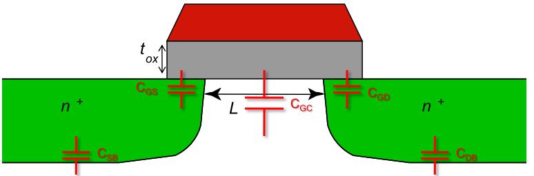
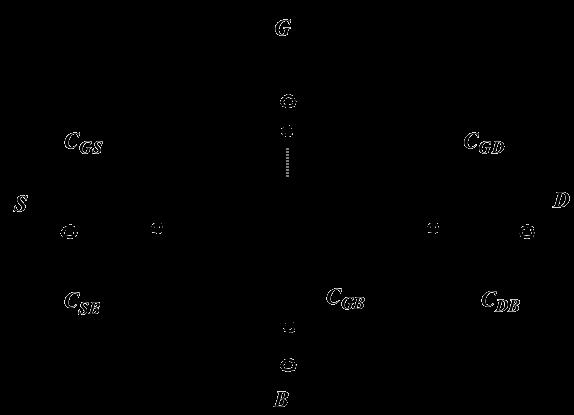
4 Gate to Channel Capacitance In general, the gate capacitance is similar to a parallel plate capacitor: A Cg Cox W L t ox However, what is the other terminal of the gate capacitance? This is dependent on the existence and characteristics of the channel. But we have to attribute the capacitance to one of the electrical terminals (i.e. G, S, D, B) of the transistor. 4
5 Gate to Channel Capacitance In cut-off, no channel exists. All capacitance is to the body: CGB Cg Cox W L C GS C GD In linear, the channel extends across the entire length. There is no capacitance to body. 0 We attribute half of the gate capacitance to the source and half to the drain. CGB CGS CGD Cg CoxWL 2 2 5
6 Gate to Channel Capacitance In saturation, the channel ends before the drain. There is no capacitance to the drain! There is still no capacitance to the body. The total capacitance is smaller than the full value. C 0 C 0 GD GB 2 2 CGS Cg Cox W L 3 3 Velocity saturation does not affect the channel. Capacitance components should be calculated according to long channel approximations! 6
7 Overlap Capacitances Overlap capacitances exist independently of the channel. The length of the overlap is deterministic, therefore: C C W L C W GD, overlap ox D, overlap D, overlap We will assume that the source and drain are equivalent. In actuality, this is layout dependent. C C C D, overlap S, overlap ov 7
8 Diffusion Capacitance Diffusion capacitance is made up of the reverse-bias capacitance of the source and drain diodes. This capacitance is voltage dependent and is proportional to the junction area of the diode. Cbottom C j W Ldiff C C W 2L sidewalls sw diff CDB CSB Cbottom Csidewalls We will usually give you this as a pre-calculated capacitance. 8
9 MOSFET Capacitances - Summary Component Cut-off Linear Saturation C GB C ox WL 0 0 C GS C ov W 0.5C ox WL + C ov W 2/3C ox WL + C ov W C GD C ov W 0.5C ox WL + C ov W C ov W C DS, C DB C diff C diff C diff 9
10 CMOS Inverter Capacitances
 We only care about the relevant capacitance during the 50% transition!")
11 Delay Capacitance Assumptions We would like to estimate the capacitance of a CMOS stage for propagation delay calculation (t pd =0.69RC) We only care about the relevant capacitance during the 50% transition! To make things easier, we will assume all capacitances are to Ground and lump them together: Driver Load C wire C C C C out out, driver wire in, load C out,1 C in,2 C int C ext C int C ext 11
12 Input and Output Capacitances Input Capacitances for CMOS gates are the Gate capacitances: C GB C GS C GD Output Capacitances for CMOS gates are the drain capacitances: C DB C GD V in G C GSP C GDP C GDN G C GSN B C GBN S C GBP D D B S C SBP C DBP V out C DBN C SBN 12
13 Driver Capacitance We will start by looking at the Output Capacitance of the Driver: C DBn is between Vout and ground. Without losing too much accuracy, we will assume that C DBp is to ground. But we have another component of the output capacitance: The feedthrough capacitance from Vin to Vout (C GDp and C GDn ). These are mainly overlap capacitances! But what is their size? V in G C GDP C GSP C GDN G C GSN B C GBN S C GBP D D B S C SBP C DBP V out C DBN C SBN C 13 out, driver Cint DBn C DBp C C C GDp GDn

14 Driver Capacitance We need to consider the Miller Effect: C GSP S V in G C GDP C GDN B C GBP D D C SBP C DBP V out C DBN So we get 2C GD,overlap G C GSN C GBN B S C SBN C 14 out, driver Cint DBn C DBp C C C 2CovWGDp n 2CGDn ovwp
15 Load Input Capacitance We look at all the capacitances connected to the gates of the load: C GSn and C GBn are between Vout and ground. Without losing much accuracy, we will assume C GSp and C GBp are to ground. Since we change from 0 to V DD /2, most of the time one transistor is cut-off, while the other is linear. So we can say that C G =C ox WL and not separate C GB, C GS and C GD. V in G C GDP C GSP C GDN G C GSN B C GBN S C GBP D D B S C SBP C DBP V out C DBN C SBN 15 C W L C oxw GSp p LCp GBp Cin, load C GSn ox n Cn GBn
16 Load Input Capacitance But what about Miller? Remember, this is a non-accurate approximation! There is very little Miller effect on the second stage because it hasn t started to switch. Considering that L=L eff +2L ov, we will usually just use C in =C ox WL. V in G C GDP C GSP C GDN B S C GBP D D C SBP C DBP V out G C GSN C GBN B S C DBN C SBN 16 Cin, load CoxWn Ln CoxWp Lp
17 CMOS Capacitances - Summary Driver Load C wire C out,1 C in,2 C int C ext C C Cout Cout, driver Cwire Cin, load int ext C C C C C W C W 2, out driver int DBn DBp ov n ov p C C FO C ext wire in, load C C W L C W L in, load ox n n ox p p 17
18 Examples
19 Exercise 1 Find the output capacitance of an inverter driving 4 identical inverters with: C C C C fF μm ; 6 ff μm ; 1.5fF; 1.15fF ov ox DBp DBn W L ; W L ; C 0.5 ff n n p p wire 19
20 Exercise 1 We ll just use the estimations we developed: C, C C 2C W 2C W out driver DBn DBp ov n ov p 1.5 ff 1.15 ff ff ff 3.58 ff C C W L C W L in,load ox n n ox p p ff 2.25 ff C C C 4 C ff out out, driver wire in, load 20
21 Exercise 1 Now find the total power consumption of the circuit operating at a frequency of 1GHz with a 2.5V supply. 1 2 C C stage C stage switch out out C 4 C out out, driver ff ff 27.4 ff P f C V 2 dyn switch DD 2 1GHz 27.4 ff 2.5V W Pstatic 0 21
22 Exercise 2: Moed B

23 Exercise 2: Moed B 2010 N1 N2 N1 cut-off N2 - linear 23
24 Exercise 2: Moed B 2010 V GN1 =V GN2 =V DD /2=0.9V N1, N2 - linear N1 N2 24
Digital Microelectronic Circuits ( )
") Digital Microelectronic ircuits (361-1-3021 ) Presented by: Dr. Alex Fish Lecture 5: Parasitic apacitance and Driving a Load 1 Motivation Thus far, we have learned how to model our essential building block,
Digital Microelectronic ircuits (361-1-3021 ) Presented by: Dr. Alex Fish Lecture 5: Parasitic apacitance and Driving a Load 1 Motivation Thus far, we have learned how to model our essential building block,
ECE321 Electronics I
 ECE31 Electronics Lecture 1: CMOS nverter: Noise Margin & Delay Model Payman Zarkesh-Ha Office: ECE Bldg. 30B Office hours: Tuesday :00-3:00PM or by appointment E-mail: payman@ece.unm.edu Slide: 1 CMOS
EEC 118 Lecture #5: CMOS Inverter AC Characteristics. Rajeevan Amirtharajah University of California, Davis Jeff Parkhurst Intel Corporation
 EEC 8 Lecture #5: CMOS Inverter AC Characteristics Rajeevan Amirtharajah University of California, Davis Jeff Parkhurst Intel Corporation Acknowledgments Slides due to Rajit Manohar from ECE 547 Advanced
EE 466/586 VLSI Design. Partha Pande School of EECS Washington State University
 EE 466/586 VLSI Design Partha Pande School of EECS Washington State University pande@eecs.wsu.edu Lecture 9 Propagation delay Power and delay Tradeoffs Follow board notes Propagation Delay Switching Time
Lecture 3: CMOS Transistor Theory
 Lecture 3: CMOS Transistor Theory Outline Introduction MOS Capacitor nmos I-V Characteristics pmos I-V Characteristics Gate and Diffusion Capacitance 2 Introduction So far, we have treated transistors
University of Pennsylvania Department of Electrical Engineering. ESE 570 Midterm Exam March 14, 2013 FORMULAS AND DATA
 University of Pennsylvania Department of Electrical Engineering ESE 570 Midterm Exam March 4, 03 FORMULAS AND DATA. PHYSICAL CONSTANTS: n i = intrinsic concentration undoped) silicon =.45 x 0 0 cm -3 @
The Physical Structure (NMOS)
") The Physical Structure (NMOS) Al SiO2 Field Oxide Gate oxide S n+ Polysilicon Gate Al SiO2 SiO2 D n+ L channel P Substrate Field Oxide contact Metal (S) n+ (G) L W n+ (D) Poly 1 Transistor Resistance Two
The Physical Structure (NMOS) Al SiO2 Field Oxide Gate oxide S n+ Polysilicon Gate Al SiO2 SiO2 D n+ L channel P Substrate Field Oxide contact Metal (S) n+ (G) L W n+ (D) Poly 1 Transistor Resistance Two
Lecture Outline. ESE 570: Digital Integrated Circuits and VLSI Fundamentals. Review: CMOS Inverter: Visual VTC. Review: CMOS Inverter: Visual VTC
 ESE 570: Digital Integrated Circuits and LSI Fundamentals Lec 0: February 4, 207 MOS Inverter: Dynamic Characteristics Lecture Outline! Review: Symmetric CMOS Inverter Design! Inverter Power! Dynamic Characteristics
Check course home page periodically for announcements. Homework 2 is due TODAY by 5pm In 240 Cory
 EE141 Fall 005 Lecture 6 MOS Capacitances, Propagation elay Important! Check course home page periodically for announcements Homework is due TOAY by 5pm In 40 Cory Homework 3 will be posted TOAY ue Thursday
ELEC 3908, Physical Electronics, Lecture 26. MOSFET Small Signal Modelling
 ELEC 3908, Physical Electronics, Lecture 26 MOSFET Small Signal Modelling Lecture Outline MOSFET small signal behavior will be considered in the same way as for the diode and BJT Capacitances will be considered
VLSI Design and Simulation
 VLSI Design and Simulation Performance Characterization Topics Performance Characterization Resistance Estimation Capacitance Estimation Inductance Estimation Performance Characterization Inverter Voltage
Integrated Circuits & Systems
 Federal University of Santa Catarina Center for Technology Computer Science & Electronics Engineering Integrated Circuits & Systems INE 5442 Lecture 13 The CMOS Inverter: dynamic behavior (delay) guntzel@inf.ufsc.br
ESE 570: Digital Integrated Circuits and VLSI Fundamentals
 ESE 570: Digital Integrated Circuits and VLSI Fundamentals Lec 10: February 15, 2018 MOS Inverter: Dynamic Characteristics Penn ESE 570 Spring 2018 Khanna Lecture Outline! Inverter Power! Dynamic Characteristics
EE115C Winter 2017 Digital Electronic Circuits. Lecture 3: MOS RC Model, CMOS Manufacturing
 EE115C Winter 2017 Digital Electronic Circuits Lecture 3: MOS RC Model, CMOS Manufacturing Agenda MOS Transistor: RC Model (pp. 104-113) S R on D CMOS Manufacturing Process (pp. 36-46) S S C GS G G C GD
Fig. 1 CMOS Transistor Circuits (a) Inverter Out = NOT In, (b) NOR-gate C = NOT (A or B)
 Inverter Out = NOT In, (b) NOR-gate C = NOT (A or B)") 1 Introduction to Transistor-Level Logic Circuits 1 By Prawat Nagvajara At the transistor level of logic circuits, transistors operate as switches with the logic variables controlling the open or closed
1 Introduction to Transistor-Level Logic Circuits 1 By Prawat Nagvajara At the transistor level of logic circuits, transistors operate as switches with the logic variables controlling the open or closed
2007 Fall: Electronic Circuits 2 CHAPTER 10. Deog-Kyoon Jeong School of Electrical Engineering
 007 Fall: Electronic Circuits CHAPTER 10 Digital CMOS Logic Circuits Deog-Kyoon Jeong dkjeong@snu.ac.kr k School of Electrical Engineering Seoul lnational luniversity it Introduction In this chapter, we
EE 330. Lecture 35. Parasitic Capacitances in MOS Devices
 EE 330 Lecture 35 Parasitic Capacitances in MOS Devices Exam 2 Wed Oct 24 Exam 3 Friday Nov 16 Review from Last Lecture Cascode Configuration Discuss V CC gm1 gm1 I B VCC V OUT g02 g01 A - β β VXX Q 2
Announcements. EE141- Fall 2002 Lecture 7. MOS Capacitances Inverter Delay Power
 - Fall 2002 Lecture 7 MOS Capacitances Inverter Delay Power Announcements Wednesday 12-3pm lab cancelled Lab 4 this week Homework 2 due today at 5pm Homework 3 posted tonight Today s lecture MOS capacitances
THE INVERTER. Inverter
 THE INVERTER DIGITAL GATES Fundamental Parameters Functionality Reliability, Robustness Area Performance» Speed (delay)» Power Consumption» Energy Noise in Digital Integrated Circuits v(t) V DD i(t) (a)
MOSFET: Introduction
 E&CE 437 Integrated VLSI Systems MOS Transistor 1 of 30 MOSFET: Introduction Metal oxide semiconductor field effect transistor (MOSFET) or MOS is widely used for implementing digital designs Its major
Integrated Circuits & Systems
 Federal University of Santa Catarina Center for Technology Computer Science & Electronics Engineering Integrated Circuits & Systems INE 5442 Lecture 14 The CMOS Inverter: dynamic behavior (sizing, inverter
ECE 342 Electronic Circuits. 3. MOS Transistors
 ECE 342 Electronic Circuits 3. MOS Transistors Jose E. Schutt-Aine Electrical & Computer Engineering University of Illinois jschutt@emlab.uiuc.edu 1 NMOS Transistor Typically L = 0.1 to 3 m, W = 0.2 to
MOS Transistor Theory
 CHAPTER 3 MOS Transistor Theory Outline 2 1. Introduction 2. Ideal I-V Characteristics 3. Nonideal I-V Effects 4. C-V Characteristics 5. DC Transfer Characteristics 6. Switch-level RC Delay Models MOS
ESE 570: Digital Integrated Circuits and VLSI Fundamentals
 ESE 570: Digital Integrated Circuits and VLSI Fundamentals Lec 10: February 16, 2016 MOS Inverter: Dynamic Characteristics Lecture Outline! Review: Symmetric CMOS Inverter Design! Inverter Power! Dynamic
MOS Transistor I-V Characteristics and Parasitics
 ECEN454 Digital Integrated Circuit Design MOS Transistor I-V Characteristics and Parasitics ECEN 454 Facts about Transistors So far, we have treated transistors as ideal switches An ON transistor passes
! MOS Capacitances. " Extrinsic. " Intrinsic. ! Lumped Capacitance Model. ! First Order Capacitor Summary. ! Capacitance Implications
 ESE 570: Digital Integrated Circuits and VLSI Fundamentals Lec 7: February, 07 MOS SPICE Models, MOS Parasitic Details Lecture Outline! MOS Capacitances " Extrinsic " Intrinsic! Lumped Capacitance Model!
Dynamic operation 20
 Dynamic operation 20 A simple model for the propagation delay Symmetric inverter (rise and fall delays are identical) otal capacitance is linear t p Minimum length devices R W C L t = 0.69R C = p W L 0.69
Lecture 210 Physical Aspects of ICs (12/15/01) Page 210-1
 Page 210-1") Lecture 210 Physical Aspects of ICs (12/15/01) Page 210-1 LECTURE 210 PHYSICAL ASPECTS OF ICs (READING: Text-Sec. 2.5, 2.6, 2.8) INTRODUCTION Objective Illustrate the physical aspects of integrated circuits
Lecture 210 Physical Aspects of ICs (12/15/01) Page 210-1 LECTURE 210 PHYSICAL ASPECTS OF ICs (READING: Text-Sec. 2.5, 2.6, 2.8) INTRODUCTION Objective Illustrate the physical aspects of integrated circuits
Digital Microelectronic Circuits ( ) The CMOS Inverter. Lecture 4: Presented by: Adam Teman
 The CMOS Inverter. Lecture 4: Presented by: Adam Teman") Digital Microelectronic Circuits (361-1-301 ) Presented by: Adam Teman Lecture 4: The CMOS Inverter 1 Last Lectures Moore s Law Terminology» Static Properties» Dynamic Properties» Power The MOSFET Transistor»
Digital Microelectronic Circuits (361-1-301 ) Presented by: Adam Teman Lecture 4: The CMOS Inverter 1 Last Lectures Moore s Law Terminology» Static Properties» Dynamic Properties» Power The MOSFET Transistor»
ECE 546 Lecture 10 MOS Transistors
 ECE 546 Lecture 10 MOS Transistors Spring 2018 Jose E. Schutt-Aine Electrical & Computer Engineering University of Illinois jesa@illinois.edu NMOS Transistor NMOS Transistor N-Channel MOSFET Built on p-type
EECS 141: FALL 05 MIDTERM 1
 University of California College of Engineering Department of Electrical Engineering and Computer Sciences D. Markovic TuTh 11-1:3 Thursday, October 6, 6:3-8:pm EECS 141: FALL 5 MIDTERM 1 NAME Last SOLUTION
ECE 438: Digital Integrated Circuits Assignment #4 Solution The Inverter
 ECE 438: Digital Integrated Circuits Assignment #4 The Inverter Text: Chapter 5, Digital Integrated Circuits 2 nd Ed, Rabaey 1) Consider the CMOS inverter circuit in Figure P1 with the following parameters.
MOS Transistor Theory
 MOS Transistor Theory So far, we have viewed a MOS transistor as an ideal switch (digital operation) Reality: less than ideal EE 261 Krish Chakrabarty 1 Introduction So far, we have treated transistors
EE105 Fall 2014 Microelectronic Devices and Circuits. NMOS Transistor Capacitances: Saturation Region
 EE105 Fall 014 Microelectronic Devices and Circuits Prof. Ming C. Wu wu@eecs.berkeley.edu 511 Sutardja Dai Hall (SDH) 1 NMOS Transistor Capacitances: Saturation Region Drain no longer connected to channel
P. R. Nelson 1 ECE418 - VLSI. Midterm Exam. Solutions
 P. R. Nelson 1 ECE418 - VLSI Midterm Exam Solutions 1. (8 points) Draw the cross-section view for A-A. The cross-section view is as shown below.. ( points) Can you tell which of the metal1 regions is the
Design of Analog Integrated Circuits
 Design of Analog Integrated Circuits Chapter 11: Introduction to Switched- Capacitor Circuits Textbook Chapter 13 13.1 General Considerations 13.2 Sampling Switches 13.3 Switched-Capacitor Amplifiers 13.4
ECE321 Electronics I
 EE31 Electronics I Lecture 8: MOSET Threshold Voltage and Parasitic apacitances Payman Zarkesh-Ha Office: EE Bldg. 3B Office hours: Tuesday :-3:PM or by appointment E-mail: payman@ece.unm.edu Slide: 1
ECE 546 Lecture 11 MOS Amplifiers
 ECE 546 Lecture MOS Amplifiers Spring 208 Jose E. Schutt-Aine Electrical & Computer Engineering University of Illinois jesa@illinois.edu ECE 546 Jose Schutt Aine Amplifiers Definitions Used to increase
ESE 570: Digital Integrated Circuits and VLSI Fundamentals
 ESE 570: Digital Integrated Circuits and VLSI Fundamentals Lec 7: February 4, 2016 MOS SPICE Models, MOS Parasitic Details Lecture Outline! MOS Capacitances " Extrinsic " Intrinsic! Lumped Capacitance
The Inverter. Digital Integrated Circuits A Design Perspective. Jan M. Rabaey Anantha Chandrakasan Borivoje Nikolic
 Digital Integrated Circuits A Design Perspective Jan M. Rabaey Anantha Chandrakasan Borivoje Nikolic The Inverter Revised from Digital Integrated Circuits, Jan M. Rabaey el, 2003 Propagation Delay CMOS
EE 435. Lecture 37. Parasitic Capacitances in MOS Devices. String DAC Parasitic Capacitances
 EE 435 Lecture 37 Parasitic Capacitances in MOS Devices String DAC Parasitic Capacitances Parasitic Capacitors in MOSFET (will initially consider two) Parasitic Capacitors in MOSFET C GCH Parasitic Capacitors
CMPEN 411 VLSI Digital Circuits Spring 2012
 CMPEN 411 VLSI Digital Circuits Spring 2012 Lecture 09: Resistance & Inverter Dynamic View [Adapted from Rabaey s Digital Integrated Circuits, Second Edition, 2003 J. Rabaey, A. Chandrakasan, B. Nikolic]
Lecture 4: CMOS Transistor Theory
 Introduction to CMOS VLSI Design Lecture 4: CMOS Transistor Theory David Harris, Harvey Mudd College Kartik Mohanram and Steven Levitan University of Pittsburgh Outline q Introduction q MOS Capacitor q
DC and Transient. Courtesy of Dr. Daehyun Dr. Dr. Shmuel and Dr.
 DC and Transient Courtesy of Dr. Daehyun Lim@WSU, Dr. Harris@HMC, Dr. Shmuel Wimer@BIU and Dr. Choi@PSU http://csce.uark.edu +1 (479) 575-604 yrpeng@uark.edu Pass Transistors We have assumed source is
Sample-and-Holds David Johns and Ken Martin University of Toronto
 Sample-and-Holds David Johns and Ken Martin (johns@eecg.toronto.edu) (martin@eecg.toronto.edu) slide 1 of 18 Sample-and-Hold Circuits Also called track-and-hold circuits Often needed in A/D converters
The Wire. Digital Integrated Circuits A Design Perspective. Jan M. Rabaey Anantha Chandrakasan Borivoje Nikolic. July 30, 2002
 Digital Integrated Circuits A Design Perspective Jan M. Rabaey Anantha Chandrakasan Borivoje Nikolic The Wire July 30, 2002 1 The Wire transmitters receivers schematics physical 2 Interconnect Impact on
and V DS V GS V T (the saturation region) I DS = k 2 (V GS V T )2 (1+ V DS )
 I DS = k 2 (V GS V T )2 (1+ V DS )") ECE 4420 Spring 2005 Page 1 FINAL EXAMINATION NAME SCORE /100 Problem 1O 2 3 4 5 6 7 Sum Points INSTRUCTIONS: This exam is closed book. You are permitted four sheets of notes (three of which are your sheets
ECE 4420 Spring 2005 Page 1 FINAL EXAMINATION NAME SCORE /100 Problem 1O 2 3 4 5 6 7 Sum Points INSTRUCTIONS: This exam is closed book. You are permitted four sheets of notes (three of which are your sheets
The transistor is not in the cutoff region. the transistor is in the saturation region. To see this, recognize that in a long-channel transistor ifv
 ECE 440 Spring 005 Page 1 Homework Assignment No. Solutions P.4 For each transistor, first determine if the transistor is in cutoff by checking to see if GS is less than or greater than. may have to be
ECE 497 JS Lecture - 12 Device Technologies
 ECE 497 JS Lecture - 12 Device Technologies Spring 2004 Jose E. Schutt-Aine Electrical & Computer Engineering University of Illinois jose@emlab.uiuc.edu 1 NMOS Transistor 2 ρ Source channel charge density
5.0 CMOS Inverter. W.Kucewicz VLSICirciuit Design 1
 5.0 CMOS Inverter W.Kucewicz VLSICirciuit Design 1 Properties Switching Threshold Dynamic Behaviour Capacitance Propagation Delay nmos/pmos Ratio Power Consumption Contents W.Kucewicz VLSICirciuit Design
ESE570 Spring University of Pennsylvania Department of Electrical and System Engineering Digital Integrated Cicruits AND VLSI Fundamentals
 University of Pennsylvania Department of Electrical and System Engineering Digital Integrated Cicruits AND VLSI Fundamentals ESE570, Spring 2018 Final Monday, Apr 0 5 Problems with point weightings shown.
Lecture 4: CMOS review & Dynamic Logic
 Lecture 4: CMOS review & Dynamic Logic Reading: ch5, ch6 Overview CMOS basics Power and energy in CMOS Dynamic logic 1 CMOS Properties Full rail-to-rail swing high noise margins Logic levels not dependent
High-to-Low Propagation Delay t PHL
 High-to-Low Propagation Delay t PHL V IN switches instantly from low to high. Driver transistor (n-channel) immediately switches from cutoff to saturation; the p-channel pull-up switches from triode to
Midterm. ESE 570: Digital Integrated Circuits and VLSI Fundamentals. Lecture Outline. Pass Transistor Logic. Restore Output.
 ESE 570: Digital Integrated Circuits and VLSI Fundamentals Lec 16: March 21, 2017 Transmission Gates, Euler Paths, Energy Basics Review Midterm! Midterm " Mean: 79.5 " Standard Dev: 14.5 2 Lecture Outline!
ECE-343 Test 2: Mar 21, :00-8:00, Closed Book. Name : SOLUTION
 ECE-343 Test 2: Mar 21, 2012 6:00-8:00, Closed Book Name : SOLUTION 1. (25 pts) (a) Draw a circuit diagram for a differential amplifier designed under the following constraints: Use only BJTs. (You may
! Inverter Power. ! Dynamic Characteristics. " Delay ! P = I V. ! Tricky part: " Understanding I. " (pairing with correct V) ! Dynamic current flow:
 ! Dynamic current flow:") ESE 570: Digital Integrated ircuits and LSI Fundamentals Lecture Outline! Inverter Power! Dynamic haracteristics Lec 10: February 15, 2018 MOS Inverter: Dynamic haracteristics " Delay 3 Power Inverter
ESE 570: Digital Integrated ircuits and LSI Fundamentals Lecture Outline! Inverter Power! Dynamic haracteristics Lec 10: February 15, 2018 MOS Inverter: Dynamic haracteristics " Delay 3 Power Inverter
Name: Grade: Q1 Q2 Q3 Q4 Q5 Total. ESE370 Fall 2015
 University of Pennsylvania Department of Electrical and System Engineering Circuit-Level Modeling, Design, and Optimization for Digital Systems ESE370, Fall 205 Midterm Wednesday, November 4 Point values
Lecture 5: DC & Transient Response
 Lecture 5: DC & Transient Response Outline q Pass Transistors q DC Response q Logic Levels and Noise Margins q Transient Response q RC Delay Models q Delay Estimation 2 Activity 1) If the width of a transistor
ESE 570: Digital Integrated Circuits and VLSI Fundamentals
 ESE 570: Digital Integrated Circuits and VLSI Fundamentals Lec 15: March 15, 2018 Euler Paths, Energy Basics and Optimization Midterm! Midterm " Mean: 89.7 " Standard Dev: 8.12 2 Lecture Outline! Euler
Lecture 10 MOSFET (III) MOSFET Equivalent Circuit Models
 MOSFET Equivalent Circuit Models") Lecture 10 MOSFET (III) MOSFET Equivalent Circuit Models Outline Lowfrequency smallsignal equivalent circuit model Highfrequency smallsignal equivalent circuit model Reading Assignment: Howe and Sodini;
Lecture 10 MOSFET (III) MOSFET Equivalent Circuit Models Outline Lowfrequency smallsignal equivalent circuit model Highfrequency smallsignal equivalent circuit model Reading Assignment: Howe and Sodini;
The Devices. Digital Integrated Circuits A Design Perspective. Jan M. Rabaey Anantha Chandrakasan Borivoje Nikolic. July 30, 2002
 Digital Integrated Circuits A Design Perspective Jan M. Rabaey Anantha Chandrakasan Borivoje Nikolic The Devices July 30, 2002 Goal of this chapter Present intuitive understanding of device operation Introduction
Lecture 12 CMOS Delay & Transient Response
 EE 471: Transport Phenomena in Solid State Devices Spring 2018 Lecture 12 CMOS Delay & Transient Response Bryan Ackland Department of Electrical and Computer Engineering Stevens Institute of Technology
CMOS Inverter (static view)
") Review: Design Abstraction Levels SYSTEM CMOS Inverter (static view) + MODULE GATE [Adapted from Chapter 5. 5.3 CIRCUIT of G DEVICE Rabaey s Digital Integrated Circuits,, J. Rabaey et al.] S D Review:
Review: Design Abstraction Levels SYSTEM CMOS Inverter (static view) + MODULE GATE [Adapted from Chapter 5. 5.3 CIRCUIT of G DEVICE Rabaey s Digital Integrated Circuits,, J. Rabaey et al.] S D Review:
ENGR890 Digital VLSI Design Fall Lecture 4: CMOS Inverter (static view)
") ENGR89 Digital VLSI Design Fall 5 Lecture 4: CMOS Inverter (static view) [Adapted from Chapter 5 of Digital Integrated Circuits, 3, J. Rabaey et al.] [Also borrowed from Vijay Narayanan and Mary Jane Irwin]
ENGR89 Digital VLSI Design Fall 5 Lecture 4: CMOS Inverter (static view) [Adapted from Chapter 5 of Digital Integrated Circuits, 3, J. Rabaey et al.] [Also borrowed from Vijay Narayanan and Mary Jane Irwin]
Topic 4. The CMOS Inverter
 Topic 4 The CMOS Inverter Peter Cheung Department of Electrical & Electronic Engineering Imperial College London URL: www.ee.ic.ac.uk/pcheung/ E-mail: p.cheung@ic.ac.uk Topic 4-1 Noise in Digital Integrated
Chapter 5. The Inverter. V1. April 10, 03 V1.1 April 25, 03 V2.1 Nov Inverter
 Chapter 5 The Inverter V1. April 10, 03 V1.1 April 25, 03 V2.1 Nov.12 03 Objective of This Chapter Use Inverter to know basic CMOS Circuits Operations Watch for performance Index such as Speed (Delay calculation)
CMPEN 411 VLSI Digital Circuits. Lecture 04: CMOS Inverter (static view)
") CMPEN 411 VLSI Digital Circuits Lecture 04: CMOS Inverter (static view) Kyusun Choi [Adapted from Rabaey s Digital Integrated Circuits, Second Edition, 2003 J. Rabaey, A. Chandrakasan, B. Nikolic] CMPEN
CMPEN 411 VLSI Digital Circuits Lecture 04: CMOS Inverter (static view) Kyusun Choi [Adapted from Rabaey s Digital Integrated Circuits, Second Edition, 2003 J. Rabaey, A. Chandrakasan, B. Nikolic] CMPEN
ENEE 359a Digital VLSI Design
 SLIDE 1 ENEE 359a Digital VLSI Design & Logical Effort Prof. blj@ece.umd.edu Credit where credit is due: Slides contain original artwork ( Jacob 2004) as well as material taken liberally from Irwin & Vijay
Lecture 13 MOSFET as an amplifier with an introduction to MOSFET small-signal model and small-signal schematics. Lena Peterson
 Lecture 13 MOSFET as an amplifier with an introduction to MOSFET small-signal model and small-signal schematics Lena Peterson 2015-10-13 Outline (1) Why is the CMOS inverter gain not infinite? Large-signal
VLSI GATE LEVEL DESIGN UNIT - III P.VIDYA SAGAR ( ASSOCIATE PROFESSOR) Department of Electronics and Communication Engineering, VBIT
 Department of Electronics and Communication Engineering, VBIT") VLSI UNIT - III GATE LEVEL DESIGN P.VIDYA SAGAR ( ASSOCIATE PROFESSOR) contents GATE LEVEL DESIGN : Logic Gates and Other complex gates, Switch logic, Alternate gate circuits, Time Delays, Driving large
VLSI UNIT - III GATE LEVEL DESIGN P.VIDYA SAGAR ( ASSOCIATE PROFESSOR) contents GATE LEVEL DESIGN : Logic Gates and Other complex gates, Switch logic, Alternate gate circuits, Time Delays, Driving large
6.012 Electronic Devices and Circuits Spring 2005
 6.012 Electronic Devices and Circuits Spring 2005 May 16, 2005 Final Exam (200 points) -OPEN BOOK- Problem NAME RECITATION TIME 1 2 3 4 5 Total General guidelines (please read carefully before starting):
ESE570 Spring University of Pennsylvania Department of Electrical and System Engineering Digital Integrated Cicruits AND VLSI Fundamentals
 University of Pennsylvania Department of Electrical and System Engineering Digital Integrated Cicruits AND VLSI Fundamentals ESE570, Spring 017 Final Wednesday, May 3 4 Problems with point weightings shown.
Step 1. Finding V M. Goal: Þnd V M = input voltage for the output = V M both transistors are saturated at V IN = V M since
 Step 1. Finding V M Goal: Þnd V M = input voltage for the output = V M both transistors are saturated at V IN = V M since V DSn = V M - 0 > V M - V Tn V SDp = V DD - V M = (V DD - V M ) V Tp Equate drain
Circuits. L2: MOS Models-2 (1 st Aug. 2013) B. Mazhari Dept. of EE, IIT Kanpur. B. Mazhari, IITK. G-Number
 B. Mazhari Dept. of EE, IIT Kanpur. B. Mazhari, IITK. G-Number") EE610: CMOS Analog Circuits L: MOS Models- (1 st Aug. 013) B. Mazhari Dept. of EE, IIT Kanpur 3 NMOS Models MOS MODEL Above Threshold Subthreshold ( GS > TN ) ( GS < TN ) Saturation ti Ti Triode ( DS >
EE610: CMOS Analog Circuits L: MOS Models- (1 st Aug. 013) B. Mazhari Dept. of EE, IIT Kanpur 3 NMOS Models MOS MODEL Above Threshold Subthreshold ( GS > TN ) ( GS < TN ) Saturation ti Ti Triode ( DS >
Last Lecture. Power Dissipation CMOS Scaling. EECS 141 S02 Lecture 8
 EECS 141 S02 Lecture 8 Power Dissipation CMOS Scaling Last Lecture CMOS Inverter loading Switching Performance Evaluation Design optimization Inverter Sizing 1 Today CMOS Inverter power dissipation» Dynamic»
EEC 116 Lecture #3: CMOS Inverters MOS Scaling. Rajeevan Amirtharajah University of California, Davis Jeff Parkhurst Intel Corporation
 EEC 116 Lecture #3: CMOS Inverters MOS Scaling Rajeevan Amirtharajah University of California, Davis Jeff Parhurst Intel Corporation Outline Review: Inverter Transfer Characteristics Lecture 3: Noise Margins,
Lecture 10 MOSFET (III) MOSFET Equivalent Circuit Models
 MOSFET Equivalent Circuit Models") Lecture 1 MOSFET (III) MOSFET Equivalent Circuit Models Outline Lowfrequency smallsignal equivalent circuit model Highfrequency smallsignal equivalent circuit model Reading Assignment: Howe and Sodini;
Lecture 1 MOSFET (III) MOSFET Equivalent Circuit Models Outline Lowfrequency smallsignal equivalent circuit model Highfrequency smallsignal equivalent circuit model Reading Assignment: Howe and Sodini;
EE 560 MOS TRANSISTOR THEORY PART 2. Kenneth R. Laker, University of Pennsylvania
 1 EE 560 MOS TRANSISTOR THEORY PART nmos TRANSISTOR IN LINEAR REGION V S = 0 V G > V T0 channel SiO V D = small 4 C GC C BC substrate depletion region or bulk B p nmos TRANSISTOR AT EDGE OF SATURATION
Digital Integrated Circuits
 Chapter 6 The CMOS Inverter 1 Contents Introduction (MOST models) 0, 1 st, 2 nd order The CMOS inverter : The static behavior: o DC transfer characteristics, o Short-circuit current The CMOS inverter :
Lecture 6 Power Zhuo Feng. Z. Feng MTU EE4800 CMOS Digital IC Design & Analysis 2010
 EE4800 CMOS Digital IC Design & Analysis Lecture 6 Power Zhuo Feng 6.1 Outline Power and Energy Dynamic Power Static Power 6.2 Power and Energy Power is drawn from a voltage source attached to the V DD
ECE-343 Test 1: Feb 10, :00-8:00pm, Closed Book. Name : SOLUTION
 ECE-343 Test : Feb 0, 00 6:00-8:00pm, Closed Book Name : SOLUTION C Depl = C J0 + V R /V o ) m C Diff = τ F g m ω T = g m C µ + C π ω T = g m I / D C GD + C or V OV GS b = τ i τ i = R i C i ω H b Z = Z
CHAPTER 15 CMOS DIGITAL LOGIC CIRCUITS
 CHAPTER 5 CMOS DIGITAL LOGIC CIRCUITS Chapter Outline 5. CMOS Logic Gate Circuits 5. Digital Logic Inverters 5.3 The CMOS Inverter 5.4 Dynamic Operation of the CMOS Inverter 5.5 Transistor Sizing 5.6 Power
EE 330 Lecture 17. MOSFET Modeling CMOS Process Flow
 EE 330 Lecture 17 MOSFET Modeling CMOS Process Flow Review from Last Lecture Limitations of Existing Models V DD V OUT V OUT V DD?? V IN V OUT V IN V IN V DD Switch-Level Models V DD Simple square-law
Switching circuits: basics and switching speed
 ECE137B notes; copyright 2018 Switching circuits: basics and switching speed Mark Rodwell, University of California, Santa Barbara Amplifiers vs. switching circuits Some transistor circuit might have V
EEC 118 Lecture #2: MOSFET Structure and Basic Operation. Rajeevan Amirtharajah University of California, Davis Jeff Parkhurst Intel Corporation
 EEC 118 Lecture #2: MOSFET Structure and Basic Operation Rajeevan Amirtharajah University of California, Davis Jeff Parkhurst Intel Corporation Announcements Lab 1 this week, report due next week Bring
Lecture 5: DC & Transient Response
 Lecture 5: DC & Transient Response Outline Pass Transistors DC Response Logic Levels and Noise Margins Transient Response RC Delay Models Delay Estimation 2 Pass Transistors We have assumed source is grounded
Answers. Name: Grade: Q1 Q2 Q3 Q4 Total mean: 83, stdev: 14. ESE370 Fall 2017
 University of Pennsylvania Department of Electrical and System Engineering Circuit-Level Modeling, Design, and Optimization for Digital Systems ESE370, Fall 2017 Midterm 2 Monday, November 6 Point values
Amplifiers, Source followers & Cascodes
 Amplifiers, Source followers & Cascodes Willy Sansen KULeuven, ESAT-MICAS Leuven, Belgium willy.sansen@esat.kuleuven.be Willy Sansen 0-05 02 Operational amplifier Differential pair v- : B v + Current mirror
Lecture 6: DC & Transient Response
 Lecture 6: DC & Transient Response Slides courtesy of Deming Chen Slides based on the initial set from David Harris CMOS VLSI Design Outline Pass Transistors DC Response Logic Levels and Noise Margins
Lecture 5: CMOS Transistor Theory
 Lecture 5: CMOS Transistor Theory Slides courtesy of Deming Chen Slides based on the initial set from David Harris CMOS VLSI Design Outline q q q q q q q Introduction MOS Capacitor nmos I-V Characteristics
Digital Integrated Circuits (83-313) Lecture 5: Interconnect. Semester B, Lecturer: Adam Teman TAs: Itamar Levi, Robert Giterman 1
 Lecture 5: Interconnect. Semester B, Lecturer: Adam Teman TAs: Itamar Levi, Robert Giterman 1") Digital Integrated Circuits (83-313) Lecture 5: Interconnect Semester B, 2015-16 Lecturer: Adam Teman TAs: Itamar Levi, Robert Giterman 1 What will we learn today? 1 A First Glance at Interconnect 2 3
Digital Integrated Circuits (83-313) Lecture 5: Interconnect Semester B, 2015-16 Lecturer: Adam Teman TAs: Itamar Levi, Robert Giterman 1 What will we learn today? 1 A First Glance at Interconnect 2 3
Digital Electronics Part II - Circuits
 Digital Electronics Part - Circuits Dr.. J. Wassell Gates from Transistors ntroduction Logic circuits are non-linear, consequently we will introduce a graphical technique for analysing such circuits The
CARNEGIE MELLON UNIVERSITY DEPARTMENT OF ELECTRICAL AND COMPUTER ENGINEERING DIGITAL INTEGRATED CIRCUITS FALL 2002
 CARNEGIE MELLON UNIVERSITY DEPARTMENT OF ELECTRICAL AND COMPUTER ENGINEERING 18-322 DIGITAL INTEGRATED CIRCUITS FALL 2002 Final Examination, Monday Dec. 16, 2002 NAME: SECTION: Time: 180 minutes Closed
LECTURE 3 MOSFETS II. MOS SCALING What is Scaling?
 LECTURE 3 MOSFETS II Lecture 3 Goals* * Understand constant field and constant voltage scaling and their effects. Understand small geometry effects for MOS transistors and their implications modeling and
Lecture 14 - Digital Circuits (III) CMOS. April 1, 2003
 CMOS. April 1, 2003") 6.12 - Microelectronic Devices and Circuits - Spring 23 Lecture 14-1 Lecture 14 - Digital Circuits (III) CMOS April 1, 23 Contents: 1. Complementary MOS (CMOS) inverter: introduction 2. CMOS inverter:
6.12 - Microelectronic Devices and Circuits - Spring 23 Lecture 14-1 Lecture 14 - Digital Circuits (III) CMOS April 1, 23 Contents: 1. Complementary MOS (CMOS) inverter: introduction 2. CMOS inverter:
The CMOS Inverter: A First Glance
 The CMOS Inverter: A First Glance V DD S D V in V out C L D S CMOS Inverter N Well V DD V DD PMOS 2λ PMOS Contacts In Out In Out Metal 1 NMOS Polysilicon NMOS GND CMOS Inverter: Steady State Response V
3. Design a stick diagram for the PMOS logic shown below [16] Y = (A + B).C. 4. Design a layout diagram for the CMOS logic shown below [16]
![3. Design a stick diagram for the PMOS logic shown below [16] Y = (A + B).C. 4. Design a layout diagram for the CMOS logic shown below [16]](/thumbs/96/128765118.jpg "3. Design a stick diagram for the PMOS logic shown below [16] Y = (A + B).C. 4. Design a layout diagram for the CMOS logic shown below [16]") Code No: RR420203 Set No. 1 1. (a) Find g m and r ds for an n-channel transistor with V GS = 1.2V; V tn = 0.8V; W/L = 10; µncox = 92 µa/v 2 and V DS = Veff + 0.5V The out put impedance constant. λ = 95.3
Code No: RR420203 Set No. 1 1. (a) Find g m and r ds for an n-channel transistor with V GS = 1.2V; V tn = 0.8V; W/L = 10; µncox = 92 µa/v 2 and V DS = Veff + 0.5V The out put impedance constant. λ = 95.3
Digital Integrated Circuits 2nd Inverter
 Digital Integrated Circuits The Inverter The CMOS Inverter V DD Analysis Inverter complex gate Cost V in V out complexity & Area Integrity and robustness C L Static behavior Performance Dynamic response
EE 330 Lecture 18. Small-signal Model (very preliminary) Bulk CMOS Process Flow
 Bulk CMOS Process Flow") EE 330 Lecture 18 Small-signal Model (very preliminary) Bulk CMOS Process Flow Review from Last Lecture How many models of the MOSFET do we have? Switch-level model (2) Square-law model Square-law model
EE 330 Lecture 18 Small-signal Model (very preliminary) Bulk CMOS Process Flow Review from Last Lecture How many models of the MOSFET do we have? Switch-level model (2) Square-law model Square-law model
Low Power VLSI Circuits and Systems Prof. Ajit Pal Department of Computer Science and Engineering Indian Institute of Technology, Kharagpur
 Low Power VLSI Circuits and Systems Prof. Ajit Pal Department of Computer Science and Engineering Indian Institute of Technology, Kharagpur Lecture No. # 08 MOS Inverters - III Hello, and welcome to today