Topics to be Covered. capacitance inductance transmission lines
|
|
|
- Harvey Cooper
- 5 years ago
- Views:
Transcription
1 Topics to be Covered Circuit Elements Switching Characteristics Power Dissipation Conductor Sizes Charge Sharing Design Margins Yield resistance capacitance inductance transmission lines
2 Resistance of uniform slabs: R = ρ L / tw ohms ρ = resistivity t = thickness Define Sheet Resistance : R S = ρ/t ohms/square R = R S (L/W) Resistance Calculations
3 Table 4.1 Typical sheet resistances for conductors Sheet Resistance ohm/sq. Material Min. Typical Max. Metal (Al) Silicides Diffusion (n+ and p+) Polysilicon CMOS3 n+ diffusion p+ diffusion * poly CMOS4S metal * Note: Doping poly p+ increases R S by approx. 40%
4 Transistor Channel Resistance In the linear region, approximate: R C = k L/W where k = [µ(ε 0 ε r /t ox ) (V GS - V t )] -1 Typical k = ohms/sq. Approximate CMOS4S: n-channel 2250 p-channel 4500
5 Contact Resistance Typical values: CMOS1B CMOS4S n+ diff contact 5-10 Ω 20 Ω p+ diff contact 5-12 Ω 20 Ω poly (n+ doped) 1 Ω 10 Ω poly (p+ doped) 5-20 Ω 10 Ω metal 1 - metal 2.12 Ω
6 Other Electrical Parameters Resistance ohms/sq. n+ diffusion 45 p+ diffusion 100 n+ poly 30 p+ poly 45 n-well 1.8k (geometry and voltage dependent) metal metal metal 1 - diffusion contacts 20 ohms (1.2 x 1.2 microns)* metal 1 - poly contacts 10 ohms (1.2 x 1.2 microns)* metal 1 - metal 2 vias ohms (1.6 x 1.6 microns)* * physical dimensions, not design scale dimensions
7 Capacitance Area Component (pf/um 2 )* Edge Component (pf/um)* metal 1 - field 2.9E E-5 metal 1 - poly 6.0E-5 metal 1 - diffusion 5.5E-5 poly - field 6.4E E-5 metal 2 - field 1.6E E-5 metal 2 - poly 2.5E-5 metal 2 - diffusion 2.0E-5 metal 2 - metal 1 5.2E-5 capacitor poly to poly 7.76E E-4 *physical dimensions, not design scale dimensions
8 MOS Capacitor Transistor Gates Silicon surface can be in one of 3 modes: 1. Accumulation (V G < 0 for n-device) C 0 = ε 0 ε ox /t ox * A (ε ox is approx. 3.9) 2. Depletion (0 < V G < V t ) Depletion layer of depth d formed under gate. d depends on gate voltage. Effect is C 0 in series with C DEP : C DEP = ε 0 ε SI (A/d) (ε SI is approx. 12) C GB = C 0 C DEP /(C 0 + C DEP ) C DEP decreases with voltage
9 3. Inversion (V G > V t ) Conductive channel restores C GB to C 0 for low frequencies only (< 100 hz) At high frequency, minority carrier mobility gets in the way and behaves like maximum inversion.
10 Transistor Parasitic Capacitance C GS, C GD C DB, C SB C GB Gate-to-channel, lumped at source/drains Diffusion-to-bulk Gate-to-bulk
11 Transistors Parasitic Capacitances (con t) Figure 4.5 Circuit symbols for parasitic capacitances
12 C a p a c i t a n c e P a r a m e t e r O f f L i n e a r S a t u r a t i o n C GB C 0 GS C 0 GD C = C + C + C G GB GS GD ε A 0 0 t OX ε A 2 ε A 2 t 2 t A 3 t ε A ε A 2 ε A t ε t OX OX 0 OX 3 t OX OX OX ε = ε 0 * ε OX i.e.: C G is approx. C 0 Typical = 0.01pF
13 Diffusion Capacitance C ja = area capacitance C jp = peripheral capacitance C D = (C ja )(ab) + (C jp )(2a + 2b) note: (ab) = area ; (2a + 2b) = perimeter *see next slide for basic structure
14 Diffusion Capacitance (con t)
15 Typical Values: C ja (pf/µm 2 ) C jp (pf/µm) MOS1S n-diff. 1 x x 10-4 MOS1S p-diff. 1 x x 10-4 CMOS3 n 4.4 x x 10-4 CMOS3 p 1.5 x x 10-4 CMOS4S n 2.9 x x 10-4 CMOS4S p 4.1 x x 10-4 note: in spice C ja = CJ and C jp = CJSW
16 Inductance Normally not a problem for on-chip wires. Can be a problem for bonding wires. On-chip L = 20 ph/mm Bonding wire and package inductance = 3-15 nh. V = LdI/dt = (5nH)(2.5mA)/(1ns) = 12.5mV Only a problem for high performance chips.
17 Metal / Poly to substrate Parallel plate model: Routing Capacitance C = (ε / t) A But fringing effect gives rise to a perimeter component similar to sidewall cap in diffusion. CMOS3 Data: C A (pf / µm 2 ) C P (pf / µm) Metal field 2.7 x x 10-4 Poly field 6.0 x x 10-4
18 Distributed RC Effect in Wires C dv dt j = (I - I ) j-1 j j-1 j j j+1 = (V - V ) R - (V - V ) R rc dv dt = d 2 V 2 dx where x = distance from input r = resistance per unit legth c = capacitance per unit length
19 Distributed RC Effect in Wires
20 Solving for propagation time of voltage step along wire of length x: t X = k x 2 Alternate solution of: t n = 1/2 (R C n(n+1)) As n = # of sections approaches infinity the alternate solution becomes: t l = 1/2 (r c l 2 ) where r = resistance per µ c = capacitance per µ l = length (µ) The result may be that it is desirable to break long signals into shorter segments with buffers inserted.
21 *continued from last slide Note: Both R and C are important here!! It is helpful to know gate caps, etc.
22 Guideline: Keep wire delay τ W well under gate delay τ G i.e.: τ W << τ G therefore l << sqrt(2 τ G / rc) For τ G = 2 nsec and typical parameters, we get the following as a guidline:
23 Switching Characteristics t r = time 10% to 90% t f = time 90% to 10% t d = delay from input transition to output transition (50%) t r = time 10% to 90% t f = time 90% to 10% t d = delay from input transition to output transition (50%)
24 Delay Time Delay of single gate dominated by output rise and fall time t dr = t r /2 t df = t f /2 Average gate delay t av = (t df +t dr )/2 = (t r + t f )/4 For more accuracy use analytical or emperical models.
25 Switching Characteristics (con t) Circuit Model:
26 Switching Characteristics (con t) Fall Time: t = 0 : V 0 = V DD V IN = 0 C L charged V IN goes to V DD p-transistor goes to off.
27 Switching Characteristics (con t)
28 Switching Characteristics (con t) Two phases: 1. T 1 saturated C L dv 0 /dt + β n /2 (V DD - V tn ) 2 = 0 V 0 >= V DD - V tn 2. T 1 linear Approximate Solution: V t = 1 V ; V DD = 5 V t f is approx. 4 C L / (β n V DD )
29 Emperical Delay Models t f = A N C L t r = A P C L β N A N and A P are derived from SPICE simulations from different transistors Note: A/B is an effective resistance, t f & t r are RC - delays Gate Delays series transistors: 1 / β eff = 1 / β / β parallel transistors: β eff = β 1 + β t f =t r requires b n = b p or W p = 2W n if L p = L n (for CMOS4S) Logic simulators will use a delay vs. load capacitance model for each type of gate. e.g.: β P
30 Thus for this gate the delay equations would be t = k r t = k f 2.12 ns (k is in pf) 3.82 ns (k is in pf)
31 Switch Level Models Model every transistor as a resistor. Simple RC s to determine delays in a circuit.
32 Switch Level Models (con t)
33 SPICE Example Transient Analysis of CMOS Inverter Note: C OUT is gates of load inverter Gate area = (3 x 3) + (3 x 5.4) = 25.2 µ 2 Gate cap = 25.2 x = pf
34
35 Cascaded Stages - It is better to drive a large load with a number of inverters (which increase in size) than with a single small inverter - Stage ratios vary from 2-10 with approx. 2.7 giving optimum speed Power Dissipation Static - Leakage currents ( na) per device P S is approx nw Dynamic - Switching transient current - Charge and discharge of load capacitance P D = C L V DD2 f P For large circuits difficult to estimate what percentage of nodes are switching, typically assume 50% if unknown
36 Conductor Sizes - Always metal power lines - Metal migration : current density < 0.25 ma/µm - Power supply noise - RC delay : power and ground bounce - Large number of small contacts (vias) when changing layers Charge Sharing C B C S - to ensure reliable charge transfer C B > 10 C S
37 Design Margins - Temperature: commercial : 0-70 o C industrial military - Supply Voltage +/- 10% - Process Variations 2-3σ : o C : o C see next slide for the diagram
38 Design Margins (con t) Figure 4.41 The distribution of process parameters
39 - Design corners - simulate circuits at all appropriate corners checking maximum speed, power, setup and hold times, timing hazards, race conditions, etc. Yield number of good chips Y= X 100% total number of chips Depends on : technology : chip area : layout
40 Two common models AD Y = e Small Chips Y > 30% Y = 1 - e AD -AD 2 Large Chips Y < 30% A = area of chip D = defect density (i.e.: lethal defects per cm 2 ) D is typically 1-5 defects per cm 2 - Yield can be improved by the incorporation of redundant structures.
41 Logic Structures - complementary static CMOS : large area : slow : always works - alternate structures : smaller : faster : increased complexity : decreased stability Example Function Z = (A B) + C
42 - pseudo NMOS 1. similar to NMOS 2. ratioed logic 3. power dissipation (static) 4. reduced noise margins 5. 1/2 transistor 6. t f smaller due to reduced load capacitance
43 - dynamic CMOS 1. precharge and evaluate phase 2. pull-down time increased 3. input can change only during recharge 4. cannot be cascaded 5. 1/2 transistors 6. dynamic (minimum clock) 7. charge redistribution
44 - domino logic 1. similar to dynamic CMOS 2. two extra transistors 3. extra inverter delay 4. stages can be cascaded 5. stages evaluate one after another (domino) 6. non-inverting structures only
45 - pass transistor logic 1. reduced transistors 2. no supply current 3. require complementary signals for inputs 4. smaller load capacitances
46 Inverter Layouts

47 Inverter Layouts (cont.)
48 NAND
49 NOR
50 Important Factors to Consider for Complex Gates Series Transistors Connections Body Effect Source-Drain Capacitance Charge Distribution
51
52 1. Series Connection

53 2. Body Effect
54 3. Source-Drain Connections
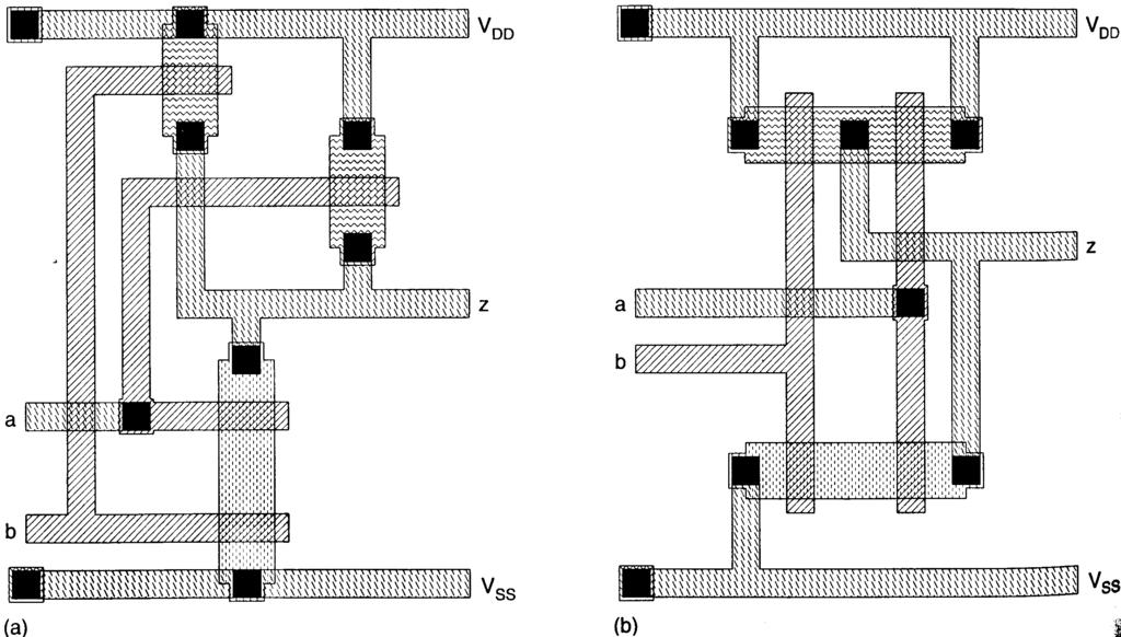
 circuit, b) poly select lines (with metal crossover)")
55 4. Charge Redistribution Routing to a transmission gate 2-input multiplexer a) circuit, b) poly select lines (with metal crossover) a) b)


56 Charge Redistribution (con t) Figure input multiplexer layouts
57 Summary complementary logic is the best option in most CMOS circuits noise immunity low DC power dissipation generally fast creation is highly automated pseudo-nmos finds use in large fan-in NOR gates e.g. ROMs, PLAs, carry look-ahead adders
58 Summary (cont.) higher static power dissipation clocked CMOS logic offers some relief for hot electron processes and conditions pass logic is fast if structures are limited to a few series transmission gates no CAD support for synthesis
59 Summary (cont.) domino logic useful for low-power high speed applications charge redistribution requires lots of simulation/development time speed advantage diminishes in poorly designed clock schemes (i.e. precharge time)
60 Pseudo 2-phase clocking: a) waveforms and special latching
61 Pseudo 2-phase clocking b) clockskew and c) slow clock edges
62 2-phase flip-flop and skew reduction
63
64 Dynamic Flip Flop
65 Static Flip-Flop
66 Static Latch
67 Static D flip-flop Table 5.5 Static D flip-flop set/reset truth table INPUTS OUTPUT CL D R S Q X X X X X X 1 1 NA
68 Recommended Clocking Approaches For first time designs that use mostly static logic, use single phase clocking and selfcontained static registers standard cells gate arrays For RAM s, ROM s and PLA s, use two phase clocking In the past, it guaranteed correct latch behaviour and dynamic latch operation
69 Recommended Clocking Approaches (cont.) Today, cycle times are very short difficult to guarantee non-overlap in all process corners Use single phase clocking for complex high-speed CMOS circuits generate special clock needs locally Use alternative clocking schemes only in special circumstances
70 I/O Pads design required detailed circuits and process knowledge use library functions pads have constant height (power connections) bonding pad 150µ x 150µ (double bond to power)
71 Pads (cont.) Types of Pads input output tristate I/O V DD GND analog
72 Pads (cont.) families of pads with different sizes ring and core supplies multiple supplies for a large number of I/O s > 40 pins 2 sets reduce noise, IR drops automatic frame programs to generate pad ring resistance and protection diodes are to prevent damage from ESD TTL requires switching threshold near 1.4volts
73 Tristate Pad
74 V DD and GND Pads simple pads made out of metal generally placed as far away from each other as possible
75 Output Pads even number of inverters size of inverters dictated by drive requirements can drive either CMOS or TTL
76 Input Pads
EE141Microelettronica. CMOS Logic
 Microelettronica CMOS Logic CMOS logic Power consumption in CMOS logic gates Where Does Power Go in CMOS? Dynamic Power Consumption Charging and Discharging Capacitors Short Circuit Currents Short Circuit
MOSFET: Introduction
 E&CE 437 Integrated VLSI Systems MOS Transistor 1 of 30 MOSFET: Introduction Metal oxide semiconductor field effect transistor (MOSFET) or MOS is widely used for implementing digital designs Its major
VLSI Design and Simulation
 VLSI Design and Simulation Performance Characterization Topics Performance Characterization Resistance Estimation Capacitance Estimation Inductance Estimation Performance Characterization Inverter Voltage
Digital Integrated Circuits A Design Perspective
 Semiconductor Memories Adapted from Chapter 12 of Digital Integrated Circuits A Design Perspective Jan M. Rabaey et al. Copyright 2003 Prentice Hall/Pearson Outline Memory Classification Memory Architectures
VLSI GATE LEVEL DESIGN UNIT - III P.VIDYA SAGAR ( ASSOCIATE PROFESSOR) Department of Electronics and Communication Engineering, VBIT
 Department of Electronics and Communication Engineering, VBIT") VLSI UNIT - III GATE LEVEL DESIGN P.VIDYA SAGAR ( ASSOCIATE PROFESSOR) contents GATE LEVEL DESIGN : Logic Gates and Other complex gates, Switch logic, Alternate gate circuits, Time Delays, Driving large
VLSI UNIT - III GATE LEVEL DESIGN P.VIDYA SAGAR ( ASSOCIATE PROFESSOR) contents GATE LEVEL DESIGN : Logic Gates and Other complex gates, Switch logic, Alternate gate circuits, Time Delays, Driving large
Digital Integrated Circuits A Design Perspective. Semiconductor. Memories. Memories
 Digital Integrated Circuits A Design Perspective Semiconductor Chapter Overview Memory Classification Memory Architectures The Memory Core Periphery Reliability Case Studies Semiconductor Memory Classification
Fig. 1 CMOS Transistor Circuits (a) Inverter Out = NOT In, (b) NOR-gate C = NOT (A or B)
 Inverter Out = NOT In, (b) NOR-gate C = NOT (A or B)") 1 Introduction to Transistor-Level Logic Circuits 1 By Prawat Nagvajara At the transistor level of logic circuits, transistors operate as switches with the logic variables controlling the open or closed
1 Introduction to Transistor-Level Logic Circuits 1 By Prawat Nagvajara At the transistor level of logic circuits, transistors operate as switches with the logic variables controlling the open or closed
MOS Transistor Theory
 CHAPTER 3 MOS Transistor Theory Outline 2 1. Introduction 2. Ideal I-V Characteristics 3. Nonideal I-V Effects 4. C-V Characteristics 5. DC Transfer Characteristics 6. Switch-level RC Delay Models MOS
Topics. Dynamic CMOS Sequential Design Memory and Control. John A. Chandy Dept. of Electrical and Computer Engineering University of Connecticut
 Topics Dynamic CMOS Sequential Design Memory and Control Dynamic CMOS In static circuits at every point in time (except when switching) the output is connected to either GND or V DD via a low resistance
MOS Transistor I-V Characteristics and Parasitics
 ECEN454 Digital Integrated Circuit Design MOS Transistor I-V Characteristics and Parasitics ECEN 454 Facts about Transistors So far, we have treated transistors as ideal switches An ON transistor passes
EE 560 CHIP INPUT AND OUTPUT (I/0) CIRCUITS. Kenneth R. Laker, University of Pennsylvania
 CIRCUITS. Kenneth R. Laker, University of Pennsylvania") 1 EE 560 CHIP INPUT AND OUTPUT (I/0) CIRCUITS 2 -> ESD PROTECTION CIRCUITS (INPUT PADS) -> ON-CHIP CLOCK GENERATION & DISTRIBUTION -> OUTPUT PADS -> ON-CHIP NOISE DUE TO PARASITIC INDUCTANCE -> SUPER BUFFER
1 EE 560 CHIP INPUT AND OUTPUT (I/0) CIRCUITS 2 -> ESD PROTECTION CIRCUITS (INPUT PADS) -> ON-CHIP CLOCK GENERATION & DISTRIBUTION -> OUTPUT PADS -> ON-CHIP NOISE DUE TO PARASITIC INDUCTANCE -> SUPER BUFFER
ESE 570: Digital Integrated Circuits and VLSI Fundamentals
 ESE 570: Digital Integrated Circuits and VLSI Fundamentals Lec 19: March 29, 2018 Memory Overview, Memory Core Cells Today! Charge Leakage/Charge Sharing " Domino Logic Design Considerations! Logic Comparisons!
Lecture 4: CMOS Transistor Theory
 Introduction to CMOS VLSI Design Lecture 4: CMOS Transistor Theory David Harris, Harvey Mudd College Kartik Mohanram and Steven Levitan University of Pittsburgh Outline q Introduction q MOS Capacitor q
and V DS V GS V T (the saturation region) I DS = k 2 (V GS V T )2 (1+ V DS )
 I DS = k 2 (V GS V T )2 (1+ V DS )") ECE 4420 Spring 2005 Page 1 FINAL EXAMINATION NAME SCORE /100 Problem 1O 2 3 4 5 6 7 Sum Points INSTRUCTIONS: This exam is closed book. You are permitted four sheets of notes (three of which are your sheets
ECE 4420 Spring 2005 Page 1 FINAL EXAMINATION NAME SCORE /100 Problem 1O 2 3 4 5 6 7 Sum Points INSTRUCTIONS: This exam is closed book. You are permitted four sheets of notes (three of which are your sheets
CMOS Digital Integrated Circuits Lec 13 Semiconductor Memories
 Lec 13 Semiconductor Memories 1 Semiconductor Memory Types Semiconductor Memories Read/Write (R/W) Memory or Random Access Memory (RAM) Read-Only Memory (ROM) Dynamic RAM (DRAM) Static RAM (SRAM) 1. Mask
S No. Questions Bloom s Taxonomy Level UNIT-I
 GROUP-A (SHORT ANSWER QUESTIONS) S No. Questions Bloom s UNIT-I 1 Define oxidation & Classify different types of oxidation Remember 1 2 Explain about Ion implantation Understand 1 3 Describe lithography
MOS Transistor Theory
 MOS Transistor Theory So far, we have viewed a MOS transistor as an ideal switch (digital operation) Reality: less than ideal EE 261 Krish Chakrabarty 1 Introduction So far, we have treated transistors
ESE 570: Digital Integrated Circuits and VLSI Fundamentals
 ESE 570: Digital Integrated Circuits and VLSI Fundamentals Lec 18: March 27, 2018 Dynamic Logic, Charge Injection Lecture Outline! Sequential MOS Logic " D-Latch " Timing Constraints! Dynamic Logic " Domino
The Physical Structure (NMOS)
") The Physical Structure (NMOS) Al SiO2 Field Oxide Gate oxide S n+ Polysilicon Gate Al SiO2 SiO2 D n+ L channel P Substrate Field Oxide contact Metal (S) n+ (G) L W n+ (D) Poly 1 Transistor Resistance Two
The Physical Structure (NMOS) Al SiO2 Field Oxide Gate oxide S n+ Polysilicon Gate Al SiO2 SiO2 D n+ L channel P Substrate Field Oxide contact Metal (S) n+ (G) L W n+ (D) Poly 1 Transistor Resistance Two
Lecture 16: Circuit Pitfalls
 Introduction to CMOS VLSI Design Lecture 16: Circuit Pitfalls David Harris Harvey Mudd College Spring 2004 Outline Pitfalls Detective puzzle Given circuit and symptom, diagnose cause and recommend solution
Lecture 23. Dealing with Interconnect. Impact of Interconnect Parasitics
 Lecture 23 Dealing with Interconnect Impact of Interconnect Parasitics Reduce Reliability Affect Performance Classes of Parasitics Capacitive Resistive Inductive 1 INTERCONNECT Dealing with Capacitance
Semiconductor Memories
 Semiconductor References: Adapted from: Digital Integrated Circuits: A Design Perspective, J. Rabaey UCB Principles of CMOS VLSI Design: A Systems Perspective, 2nd Ed., N. H. E. Weste and K. Eshraghian
! Charge Leakage/Charge Sharing. " Domino Logic Design Considerations. ! Logic Comparisons. ! Memory. " Classification. " ROM Memories.
 ESE 57: Digital Integrated Circuits and VLSI Fundamentals Lec 9: March 9, 8 Memory Overview, Memory Core Cells Today! Charge Leakage/ " Domino Logic Design Considerations! Logic Comparisons! Memory " Classification
Semiconductor memories
 Semiconductor memories Semiconductor Memories Data in Write Memory cell Read Data out Some design issues : How many cells? Function? Power consuption? Access type? How fast are read/write operations? Semiconductor
Chapter 5 CMOS Logic Gate Design
 Chapter 5 CMOS Logic Gate Design Section 5. -To achieve correct operation of integrated logic gates, we need to satisfy 1. Functional specification. Temporal (timing) constraint. (1) In CMOS, incorrect
CMOS Logic Gates. University of Connecticut 172
 CMOS Logic Gates University of Connecticut 172 Basic CMOS Inverter Operation V IN P O N O p-channel enhancementtype MOSFET; V T < 0 n-channel enhancementtype MOSFET; V T > 0 If V IN 0, N O is cut off and
Lecture 12 CMOS Delay & Transient Response
 EE 471: Transport Phenomena in Solid State Devices Spring 2018 Lecture 12 CMOS Delay & Transient Response Bryan Ackland Department of Electrical and Computer Engineering Stevens Institute of Technology
THE INVERTER. Inverter
 THE INVERTER DIGITAL GATES Fundamental Parameters Functionality Reliability, Robustness Area Performance» Speed (delay)» Power Consumption» Energy Noise in Digital Integrated Circuits v(t) V DD i(t) (a)
Low Power VLSI Circuits and Systems Prof. Ajit Pal Department of Computer Science and Engineering Indian Institute of Technology, Kharagpur
 Low Power VLSI Circuits and Systems Prof. Ajit Pal Department of Computer Science and Engineering Indian Institute of Technology, Kharagpur Lecture No. # 08 MOS Inverters - III Hello, and welcome to today
ENEE 359a Digital VLSI Design
 SLIDE 1 ENEE 359a Digital VLSI Design & Logical Effort Prof. blj@ece.umd.edu Credit where credit is due: Slides contain original artwork ( Jacob 2004) as well as material taken liberally from Irwin & Vijay
Digital Integrated Circuits Designing Combinational Logic Circuits. Fuyuzhuo
 Digital Integrated Circuits Designing Combinational Logic Circuits Fuyuzhuo Introduction Digital IC Dynamic Logic Introduction Digital IC EE141 2 Dynamic logic outline Dynamic logic principle Dynamic logic
GMU, ECE 680 Physical VLSI Design 1
 ECE680: Physical VLSI Design Chapter VIII Semiconductor Memory (chapter 12 in textbook) 1 Chapter Overview Memory Classification Memory Architectures The Memory Core Periphery Reliability Case Studies
University of Pennsylvania Department of Electrical Engineering. ESE 570 Midterm Exam March 14, 2013 FORMULAS AND DATA
 University of Pennsylvania Department of Electrical Engineering ESE 570 Midterm Exam March 4, 03 FORMULAS AND DATA. PHYSICAL CONSTANTS: n i = intrinsic concentration undoped) silicon =.45 x 0 0 cm -3 @
SEMICONDUCTOR MEMORIES
 SEMICONDUCTOR MEMORIES Semiconductor Memory Classification RWM NVRWM ROM Random Access Non-Random Access EPROM E 2 PROM Mask-Programmed Programmable (PROM) SRAM FIFO FLASH DRAM LIFO Shift Register CAM
Interconnect (2) Buffering Techniques.Transmission Lines. Lecture Fall 2003
 Buffering Techniques.Transmission Lines. Lecture Fall 2003") Interconnect (2) Buffering Techniques.Transmission Lines Lecture 12 18-322 Fall 2003 A few announcements Partners Lab Due Times Midterm 1 is nearly here Date: 10/14/02, time: 3:00-4:20PM, place: in class
Interconnect (2) Buffering Techniques.Transmission Lines Lecture 12 18-322 Fall 2003 A few announcements Partners Lab Due Times Midterm 1 is nearly here Date: 10/14/02, time: 3:00-4:20PM, place: in class
The Devices. Devices
 The The MOS Transistor Gate Oxyde Gate Source n+ Polysilicon Drain n+ Field-Oxyde (SiO 2 ) p-substrate p+ stopper Bulk Contact CROSS-SECTION of NMOS Transistor Cross-Section of CMOS Technology MOS transistors
COMBINATIONAL LOGIC. Combinational Logic
 COMINTIONL LOGIC Overview Static CMOS Conventional Static CMOS Logic Ratioed Logic Pass Transistor/Transmission Gate Logic Dynamic CMOS Logic Domino np-cmos Combinational vs. Sequential Logic In Logic
Electronic Devices and Circuits Lecture 15 - Digital Circuits: Inverter Basics - Outline Announcements. = total current; I D
 6.012 - Electronic Devices and Circuits Lecture 15 - Digital Circuits: Inverter asics - Outline Announcements Handout - Lecture Outline and Summary The MOSFET alpha factor - use definition in lecture,
ECE 546 Lecture 10 MOS Transistors
 ECE 546 Lecture 10 MOS Transistors Spring 2018 Jose E. Schutt-Aine Electrical & Computer Engineering University of Illinois jesa@illinois.edu NMOS Transistor NMOS Transistor N-Channel MOSFET Built on p-type
9/18/2008 GMU, ECE 680 Physical VLSI Design
 ECE680: Physical VLSI Design Chapter III CMOS Device, Inverter, Combinational circuit Logic and Layout Part 3 Combinational Logic Gates (textbook chapter 6) 9/18/2008 GMU, ECE 680 Physical VLSI Design
Digital Integrated Circuits A Design Perspective
 Digital Integrated Circuits Design Perspective Designing Combinational Logic Circuits Fuyuzhuo School of Microelectronics,SJTU Introduction Digital IC Dynamic Logic Introduction Digital IC 2 EE141 Dynamic
Dynamic Combinational Circuits. Dynamic Logic
 Dynamic Combinational Circuits Dynamic circuits Charge sharing, charge redistribution Domino logic np-cmos (zipper CMOS) Krish Chakrabarty 1 Dynamic Logic Dynamic gates use a clocked pmos pullup Two modes:
Lecture 5. MOS Inverter: Switching Characteristics and Interconnection Effects
 Lecture 5 MOS Inverter: Switching Characteristics and Interconnection Effects Introduction C load = (C gd,n + C gd,p + C db,n + C db,p ) + (C int + C g ) Lumped linear capacitance intrinsic cap. extrinsic
Hw 6 and 7 Graded and available Project Phase 2 Graded Project Phase 3 Launch Today
 EECS141 1 Hw 8 Posted Last one to be graded Due Friday April 30 Hw 6 and 7 Graded and available Project Phase 2 Graded Project Phase 3 Launch Today EECS141 2 1 6 5 4 3 2 1 0 1.5 2 2.5 3 3.5 4 Frequency
EECS 141 F01 Lecture 17
 EECS 4 F0 Lecture 7 With major inputs/improvements From Mary-Jane Irwin (Penn State) Dynamic CMOS In static circuits at every point in time (except when switching) the output is connected to either GND
CMOS Logic Gates. University of Connecticut 181
 CMOS Logic Gates University of Connecticut 181 Basic CMOS Inverter Operation V IN P O N O p-channel enhancementtype MOSFET; V T < 0 n-channel enhancementtype MOSFET; V T > 0 If V IN 0, N O is cut off and
EE115C Winter 2017 Digital Electronic Circuits. Lecture 3: MOS RC Model, CMOS Manufacturing
 EE115C Winter 2017 Digital Electronic Circuits Lecture 3: MOS RC Model, CMOS Manufacturing Agenda MOS Transistor: RC Model (pp. 104-113) S R on D CMOS Manufacturing Process (pp. 36-46) S S C GS G G C GD
CARNEGIE MELLON UNIVERSITY DEPARTMENT OF ELECTRICAL AND COMPUTER ENGINEERING DIGITAL INTEGRATED CIRCUITS FALL 2002
 CARNEGIE MELLON UNIVERSITY DEPARTMENT OF ELECTRICAL AND COMPUTER ENGINEERING 18-322 DIGITAL INTEGRATED CIRCUITS FALL 2002 Final Examination, Monday Dec. 16, 2002 NAME: SECTION: Time: 180 minutes Closed
Lecture 3: CMOS Transistor Theory
 Lecture 3: CMOS Transistor Theory Outline Introduction MOS Capacitor nmos I-V Characteristics pmos I-V Characteristics Gate and Diffusion Capacitance 2 Introduction So far, we have treated transistors
The Devices: MOS Transistors
 The Devices: MOS Transistors References: Semiconductor Device Fundamentals, R. F. Pierret, Addison-Wesley Digital Integrated Circuits: A Design Perspective, J. Rabaey et.al. Prentice Hall NMOS Transistor
ESE570 Spring University of Pennsylvania Department of Electrical and System Engineering Digital Integrated Cicruits AND VLSI Fundamentals
 University of Pennsylvania Department of Electrical and System Engineering Digital Integrated Cicruits AND VLSI Fundamentals ESE570, Spring 017 Final Wednesday, May 3 4 Problems with point weightings shown.
Static CMOS Circuits. Example 1
 Static CMOS Circuits Conventional (ratio-less) static CMOS Covered so far Ratio-ed logic (depletion load, pseudo nmos) Pass transistor logic ECE 261 Krish Chakrabarty 1 Example 1 module mux(input s, d0,
CMOS Inverter (static view)
") Review: Design Abstraction Levels SYSTEM CMOS Inverter (static view) + MODULE GATE [Adapted from Chapter 5. 5.3 CIRCUIT of G DEVICE Rabaey s Digital Integrated Circuits,, J. Rabaey et al.] S D Review:
Review: Design Abstraction Levels SYSTEM CMOS Inverter (static view) + MODULE GATE [Adapted from Chapter 5. 5.3 CIRCUIT of G DEVICE Rabaey s Digital Integrated Circuits,, J. Rabaey et al.] S D Review:
Semiconductor Memory Classification
 Semiconductor Memory Classification Read-Write Memory Non-Volatile Read-Write Memory Read-Only Memory Random Access Non-Random Access EPROM E 2 PROM Mask-Programmed Programmable (PROM) SRAM FIFO FLASH
Lecture 5: CMOS Transistor Theory
 Lecture 5: CMOS Transistor Theory Slides courtesy of Deming Chen Slides based on the initial set from David Harris CMOS VLSI Design Outline q q q q q q q Introduction MOS Capacitor nmos I-V Characteristics
Spiral 2 7. Capacitance, Delay and Sizing. Mark Redekopp
 2-7.1 Spiral 2 7 Capacitance, Delay and Sizing Mark Redekopp 2-7.2 Learning Outcomes I understand the sources of capacitance in CMOS circuits I understand how delay scales with resistance, capacitance
Device Models (PN Diode, MOSFET )
") Device Models (PN Diode, MOSFET ) Instructor: Steven P. Levitan steve@ece.pitt.edu TA: Gayatri Mehta, José Martínez Book: Digital Integrated Circuits: A Design Perspective; Jan Rabaey Lab Notes: Handed
Device Models (PN Diode, MOSFET ) Instructor: Steven P. Levitan steve@ece.pitt.edu TA: Gayatri Mehta, José Martínez Book: Digital Integrated Circuits: A Design Perspective; Jan Rabaey Lab Notes: Handed
Lecture 7 Circuit Delay, Area and Power
 Lecture 7 Circuit Delay, Area and Power lecture notes from S. Mitra Intro VLSI System course (EE271) Introduction to VLSI Systems 1 Circuits and Delay Introduction to VLSI Systems 2 Power, Delay and Area:
Chapter 2 CMOS Transistor Theory. Jin-Fu Li Department of Electrical Engineering National Central University Jungli, Taiwan
 Chapter 2 CMOS Transistor Theory Jin-Fu Li Department of Electrical Engineering National Central University Jungli, Taiwan Outline Introduction MOS Device Design Equation Pass Transistor Jin-Fu Li, EE,
ECE 497 JS Lecture - 12 Device Technologies
 ECE 497 JS Lecture - 12 Device Technologies Spring 2004 Jose E. Schutt-Aine Electrical & Computer Engineering University of Illinois jose@emlab.uiuc.edu 1 NMOS Transistor 2 ρ Source channel charge density
Lecture 25. Semiconductor Memories. Issues in Memory
 Lecture 25 Semiconductor Memories Issues in Memory Memory Classification Memory Architectures TheMemoryCore Periphery 1 Semiconductor Memory Classification RWM NVRWM ROM Random Access Non-Random Access
EEC 118 Lecture #6: CMOS Logic. Rajeevan Amirtharajah University of California, Davis Jeff Parkhurst Intel Corporation
 EEC 118 Lecture #6: CMOS Logic Rajeevan mirtharajah University of California, Davis Jeff Parkhurst Intel Corporation nnouncements Quiz 1 today! Lab 2 reports due this week Lab 3 this week HW 3 due this
ENEE 359a Digital VLSI Design
 SLIDE 1 ENEE 359a Digital VLSI Design Prof. blj@eng.umd.edu Credit where credit is due: Slides contain original artwork ( Jacob 2004) as well as material taken liberally from Irwin & Vijay s CSE477 slides
KINGS COLLEGE OF ENGINEERING DEPARTMENT OF ELECTRONICS AND COMMUNICATION ENGINEERING QUESTION BANK
 KINGS COLLEGE OF ENGINEERING DEPARTMENT OF ELECTRONICS AND COMMUNICATION ENGINEERING QUESTION BANK SUBJECT CODE: EC 1354 SUB.NAME : VLSI DESIGN YEAR / SEMESTER: III / VI UNIT I MOS TRANSISTOR THEORY AND
MM74C150 MM82C19 16-Line to 1-Line Multiplexer 3-STATE 16-Line to 1-Line Multiplexer
 MM74C150 MM82C19 16-Line to 1-Line Multiplexer 3-STATE 16-Line to 1-Line Multiplexer General Description The MM74C150 and MM82C19 multiplex 16 digital lines to 1 output. A 4-bit address code determines
Interconnects. Wire Resistance Wire Capacitance Wire RC Delay Crosstalk Wire Engineering Repeaters. ECE 261 James Morizio 1
 Interconnects Wire Resistance Wire Capacitance Wire RC Delay Crosstalk Wire Engineering Repeaters ECE 261 James Morizio 1 Introduction Chips are mostly made of wires called interconnect In stick diagram,
Announcements. EE141- Fall 2002 Lecture 25. Interconnect Effects I/O, Power Distribution
 - Fall 2002 Lecture 25 Interconnect Effects I/O, Power Distribution Announcements Homework 9 due next Tuesday Hardware lab this week Project phase 2 due in two weeks 1 Today s Lecture Impact of interconnects»
Dynamic Combinational Circuits. Dynamic Logic
 Dynamic Combinational Circuits Dynamic circuits Charge sharing, charge redistribution Domino logic np-cmos (zipper CMOS) Krish Chakrabarty 1 Dynamic Logic Dynamic gates use a clocked pmos pullup Two modes:
Lecture 5: DC & Transient Response
 Lecture 5: DC & Transient Response Outline q Pass Transistors q DC Response q Logic Levels and Noise Margins q Transient Response q RC Delay Models q Delay Estimation 2 Activity 1) If the width of a transistor
EE141- Fall 2002 Lecture 27. Memory EE141. Announcements. We finished all the labs No homework this week Projects are due next Tuesday 9am EE141
 - Fall 2002 Lecture 27 Memory Announcements We finished all the labs No homework this week Projects are due next Tuesday 9am 1 Today s Lecture Memory:» SRAM» DRAM» Flash Memory 2 Floating-gate transistor
Miscellaneous Lecture topics. Mary Jane Irwin [Adapted from Rabaey s Digital Integrated Circuits, 2002, J. Rabaey et al.]
![Miscellaneous Lecture topics. Mary Jane Irwin [Adapted from Rabaey s Digital Integrated Circuits, 2002, J. Rabaey et al.]](/thumbs/81/84503671.jpg "Miscellaneous Lecture topics. Mary Jane Irwin [Adapted from Rabaey s Digital Integrated Circuits, 2002, J. Rabaey et al.]") Miscellaneous Lecture topics Mary Jane Irwin [dapted from Rabaey s Digital Integrated Circuits, 2002, J. Rabaey et al.] MOS Switches MOS transistors can be viewed as simple switches. In an N-Switch, the
Miscellaneous Lecture topics Mary Jane Irwin [dapted from Rabaey s Digital Integrated Circuits, 2002, J. Rabaey et al.] MOS Switches MOS transistors can be viewed as simple switches. In an N-Switch, the
EEC 116 Lecture #5: CMOS Logic. Rajeevan Amirtharajah Bevan Baas University of California, Davis Jeff Parkhurst Intel Corporation
 EEC 116 Lecture #5: CMOS Logic Rajeevan mirtharajah Bevan Baas University of California, Davis Jeff Parkhurst Intel Corporation nnouncements Quiz 1 today! Lab 2 reports due this week Lab 3 this week HW
Digital Integrated Circuits A Design Perspective
 Designing ombinational Logic ircuits dapted from hapter 6 of Digital Integrated ircuits Design Perspective Jan M. Rabaey et al. opyright 2003 Prentice Hall/Pearson 1 ombinational vs. Sequential Logic In
NTE74HC173 Integrated Circuit TTL High Speed CMOS, 4 Bit D Type Flip Flop with 3 State Outputs
 NTE74HC173 Integrated Circuit TTL High Speed CMOS, 4 Bit D Type Flip Flop with 3 State Outputs Description: The NTE74HC173 is an high speed 3 State Quad D Type Flip Flop in a 16 Lead DIP type package that
The Wire. Digital Integrated Circuits A Design Perspective. Jan M. Rabaey Anantha Chandrakasan Borivoje Nikolic. July 30, 2002
 Digital Integrated Circuits A Design Perspective Jan M. Rabaey Anantha Chandrakasan Borivoje Nikolic The Wire July 30, 2002 1 The Wire transmitters receivers schematics physical 2 Interconnect Impact on
Introduction to CMOS VLSI. Chapter 2: CMOS Transistor Theory. Harris, 2004 Updated by Li Chen, Outline
 Introduction to MOS VLSI Design hapter : MOS Transistor Theory copyright@david Harris, 004 Updated by Li hen, 010 Outline Introduction MOS apacitor nmos IV haracteristics pmos IV haracteristics Gate and
ECE 438: Digital Integrated Circuits Assignment #4 Solution The Inverter
 ECE 438: Digital Integrated Circuits Assignment #4 The Inverter Text: Chapter 5, Digital Integrated Circuits 2 nd Ed, Rabaey 1) Consider the CMOS inverter circuit in Figure P1 with the following parameters.
MOSFET and CMOS Gate. Copy Right by Wentai Liu
 MOSFET and CMOS Gate CMOS Inverter DC Analysis - Voltage Transfer Curve (VTC) Find (1) (2) (3) (4) (5) (6) V OH min, V V OL min, V V IH min, V V IL min, V OHmax OLmax IHmax ILmax NM L = V ILmax V OL max
Switched-Capacitor Circuits David Johns and Ken Martin University of Toronto
 Switched-Capacitor Circuits David Johns and Ken Martin University of Toronto (johns@eecg.toronto.edu) (martin@eecg.toronto.edu) University of Toronto 1 of 60 Basic Building Blocks Opamps Ideal opamps usually
Semiconductor Memories
 !"#"$%&'()$*#+%$*,' -"+./"$0 1'!*0"#)'2*+03*.$"4* Jan M. Rabaey Anantha Chandrakasan Borivoje Nikolic Semiconductor Memories December 20, 2002 !"#$%&'()*&'*+&, Memory Classification Memory Architectures
ESE 570: Digital Integrated Circuits and VLSI Fundamentals
 ESE 570: Digital Integrated Circuits and VLSI Fundamentals Lec 7: February 4, 2016 MOS SPICE Models, MOS Parasitic Details Lecture Outline! MOS Capacitances " Extrinsic " Intrinsic! Lumped Capacitance
Homework Assignment #5 EE 477 Spring 2017 Professor Parker
 Homework Assignment #5 EE 477 Spring 2017 Professor Parker Question 1: (15%) Compute the worst-case rising and falling RC time constants at point B of the circuit below using the Elmore delay method. Assume
DC and Transient. Courtesy of Dr. Daehyun Dr. Dr. Shmuel and Dr.
 DC and Transient Courtesy of Dr. Daehyun Lim@WSU, Dr. Harris@HMC, Dr. Shmuel Wimer@BIU and Dr. Choi@PSU http://csce.uark.edu +1 (479) 575-604 yrpeng@uark.edu Pass Transistors We have assumed source is
3. Design a stick diagram for the PMOS logic shown below [16] Y = (A + B).C. 4. Design a layout diagram for the CMOS logic shown below [16]
![3. Design a stick diagram for the PMOS logic shown below [16] Y = (A + B).C. 4. Design a layout diagram for the CMOS logic shown below [16]](/thumbs/96/128765118.jpg "3. Design a stick diagram for the PMOS logic shown below [16] Y = (A + B).C. 4. Design a layout diagram for the CMOS logic shown below [16]") Code No: RR420203 Set No. 1 1. (a) Find g m and r ds for an n-channel transistor with V GS = 1.2V; V tn = 0.8V; W/L = 10; µncox = 92 µa/v 2 and V DS = Veff + 0.5V The out put impedance constant. λ = 95.3
Code No: RR420203 Set No. 1 1. (a) Find g m and r ds for an n-channel transistor with V GS = 1.2V; V tn = 0.8V; W/L = 10; µncox = 92 µa/v 2 and V DS = Veff + 0.5V The out put impedance constant. λ = 95.3
Lecture 12: MOS Capacitors, transistors. Context
 Lecture 12: MOS Capacitors, transistors Context In the last lecture, we discussed PN diodes, and the depletion layer into semiconductor surfaces. Small signal models In this lecture, we will apply those
Objective and Outline. Acknowledgement. Objective: Power Components. Outline: 1) Acknowledgements. Section 4: Power Components
 Acknowledgements. Section 4: Power Components") Objective: Power Components Outline: 1) Acknowledgements 2) Objective and Outline 1 Acknowledgement This lecture note has been obtained from similar courses all over the world. I wish to thank all the
Objective: Power Components Outline: 1) Acknowledgements 2) Objective and Outline 1 Acknowledgement This lecture note has been obtained from similar courses all over the world. I wish to thank all the
Chapter 4 Field-Effect Transistors
 Chapter 4 Field-Effect Transistors Microelectronic Circuit Design Richard C. Jaeger Travis N. Blalock 5/5/11 Chap 4-1 Chapter Goals Describe operation of MOSFETs. Define FET characteristics in operation
ESE 570: Digital Integrated Circuits and VLSI Fundamentals
 ESE 570: Digital Integrated Circuits and VLSI Fundamentals Lec 24: April 19, 2018 Crosstalk and Wiring, Transmission Lines Lecture Outline! Crosstalk! Repeaters in Wiring! Transmission Lines " Where transmission
! MOS Capacitances. " Extrinsic. " Intrinsic. ! Lumped Capacitance Model. ! First Order Capacitor Summary. ! Capacitance Implications
 ESE 570: Digital Integrated Circuits and VLSI Fundamentals Lec 7: February, 07 MOS SPICE Models, MOS Parasitic Details Lecture Outline! MOS Capacitances " Extrinsic " Intrinsic! Lumped Capacitance Model!
Clock Strategy. VLSI System Design NCKUEE-KJLEE
 Clock Strategy Clocked Systems Latch and Flip-flops System timing Clock skew High speed latch design Phase locked loop ynamic logic Multiple phase Clock distribution Clocked Systems Most VLSI systems are
ECE 342 Electronic Circuits. 3. MOS Transistors
 ECE 342 Electronic Circuits 3. MOS Transistors Jose E. Schutt-Aine Electrical & Computer Engineering University of Illinois jschutt@emlab.uiuc.edu 1 NMOS Transistor Typically L = 0.1 to 3 m, W = 0.2 to
CMOS INVERTER. Last Lecture. Metrics for qualifying digital circuits. »Cost» Reliability» Speed (delay)»performance
»performance") CMOS INVERTER Last Lecture Metrics for qualifying digital circuits»cost» Reliability» Speed (delay)»performance 1 Today s lecture The CMOS inverter at a glance An MOS transistor model for manual analysis
CMOS INVERTER Last Lecture Metrics for qualifying digital circuits»cost» Reliability» Speed (delay)»performance 1 Today s lecture The CMOS inverter at a glance An MOS transistor model for manual analysis
EE 466/586 VLSI Design. Partha Pande School of EECS Washington State University
 EE 466/586 VLSI Design Partha Pande School of EECS Washington State University pande@eecs.wsu.edu Lecture 8 Power Dissipation in CMOS Gates Power in CMOS gates Dynamic Power Capacitance switching Crowbar
EEC 118 Lecture #2: MOSFET Structure and Basic Operation. Rajeevan Amirtharajah University of California, Davis Jeff Parkhurst Intel Corporation
 EEC 118 Lecture #2: MOSFET Structure and Basic Operation Rajeevan Amirtharajah University of California, Davis Jeff Parkhurst Intel Corporation Announcements Lab 1 this week, report due next week Bring
EE241 - Spring 2000 Advanced Digital Integrated Circuits. Announcements
 EE241 - Spring 2 Advanced Digital Integrated Circuits Lecture 11 Low Power-Low Energy Circuit Design Announcements Homework #2 due Friday, 3/3 by 5pm Midterm project reports due in two weeks - 3/7 by 5pm
Digital Integrated Circuits. The Wire * Fuyuzhuo. *Thanks for Dr.Guoyong.SHI for his slides contributed for the talk. Digital IC.
 Digital Integrated Circuits The Wire * Fuyuzhuo *Thanks for Dr.Guoyong.SHI for his slides contributed for the talk Introduction The Wire transmitters receivers schematics physical 2 Interconnect Impact
NTE4514B & NTE4515B Integrated Circuit CMOS, 4 Bit Latch/4 to 16 Line Decoder
 NTE4514B & NTE4515B Integrated Circuit CMOS, 4 Bit Latch/4 to 16 Line Decoder Description: The NTE4514B (output active high option) and NTE4515B (output active low option) are two output options of a 4
Lecture 34: Portable Systems Technology Background Professor Randy H. Katz Computer Science 252 Fall 1995
 Lecture 34: Portable Systems Technology Background Professor Randy H. Katz Computer Science 252 Fall 1995 RHK.F95 1 Technology Trends: Microprocessor Capacity 100000000 10000000 Pentium Transistors 1000000
! Crosstalk. ! Repeaters in Wiring. ! Transmission Lines. " Where transmission lines arise? " Lossless Transmission Line.
 ESE 570: Digital Integrated Circuits and VLSI Fundamentals Lec 24: April 19, 2018 Crosstalk and Wiring, Transmission Lines Lecture Outline! Crosstalk! Repeaters in Wiring! Transmission Lines " Where transmission
Digital Electronics Part II - Circuits
 Digital Electronics Part - Circuits Dr.. J. Wassell Gates from Transistors ntroduction Logic circuits are non-linear, consequently we will introduce a graphical technique for analysing such circuits The