MOS Amplifiers Dr. Lynn Fuller Webpage:
|
|
|
- Tabitha Anderson
- 5 years ago
- Views:
Transcription
1 ROCHESTER INSTITUTE OF TECHNOLOGY MICROELECTRONIC ENGINEERING Dr. Lynn Fuller Webpage: 82 Lomb Memorial Drive Rochester, NY Department webpage: MOS_Amplifiers.ppt Page 1
2 OUTLINE Introduction Voltage Transfer Curve (VTC) NMOS Inverting Amplifier Resistor Load NMOS Enhancement Load NMOS Enhancement V++ NMOS Depletion Load CMOS Biasing The Amplifier Resistor RG Feedback Resistor from Vout to Vin References Homework Appendix SPICE Models Cadence Parameter Sweeps Page 2
3 INTRODUCTION There are many ways to make an inverting amplifier. Lets start with the common source with resistor load inverting amplifier. The voltage transfer curve, VTC (Vout vs Vin) shows where large change in Vout vs Vin occurs and if the circuit is biased in this region we can realize a voltage amplifier. Vin Vout R +V Vout +V Vout Slope = Gain SYMBOL Vin RESISTOR LOAD 0 0 VTC +Vin Page 3
4 VIN CALCULATION OF VOLTAGE TRANSFER CURVE R +V DD VOUT NMOS-M1 RESISTOR LOAD First figure out if the transistor is sub-threshold or off, Vgs < Vth and Vgd < Vth non-saturation, Vgs > Vth and Vgd > Vth saturation region, Vgs > Vth and Vgd < Vth Note: Rochester Vin Institute = Vgs, of Technology Vout = Vds, therefore Vgd = Vin-Vout Vth might be +1volt +V 0 VOUT 0 M1 Off Vth M1 Saturation M1 Linear VTC +V VIN Page 4
5 CALCULATION OF VTC VIN R +V DD I D VOUT NMOS-M1 RESISTOR LOAD Next calculate Vout = V DD I D R using the correct equation for I D for the transistor depending on region of operation Linear (Non-Saturation) I D = µw Cox (Vg-Vt-V d /2)V d L +V 0 VOUT 0 M1 Off Vth M1 Saturation Cox = Cox/Area = o r/xox M1 Linear Saturation +V VIN I D = µw Cox (Vg-Vt) 2 2L Page 5
6 CALCULATION OF VTC M1 in Saturation Vout = V DD R I D = Given: V DD and R We know the following: Cox = Cox/Area = o r/xox o = 8.85e-14 F/cm r=3.9 for oxide Xox = gate oxide thickness W= width of MOSFET L=Length of MOSFET Vt = Threshold Voltage µ = mobility V DD - R µw Cox (Vin-Vt) 2 2L Page 6
7 CALCULATION OF VTC M1 in Non-Saturation Vout = V DD I D R Vout = V DD I D R = V DD - R µw Cox (Vg-Vt-V d /2)V d L Kx Vo = V DD - R Kx(Vin-Vt-Vo/2)Vo Vo = V DD - R Kx(Vin-Vt)Vo- RKxVo 2 /2 quadratic formula 0 = V DD - R Kx(Vin-Vt - 1)Vo- RKxVo 2 /2 a x 2 + bx + c = 0 x = -b +/- b 2-4ac 2a Page 7
8 CALCULATION OF VTC M1 in Non-Saturation Vout = b +/- b 2-2V DD /KxR b=(vin Vt + 1/KxR) 2a Page 8

9 CALCULATION OF VTC Note: Equations only valid in specific regions Page 9

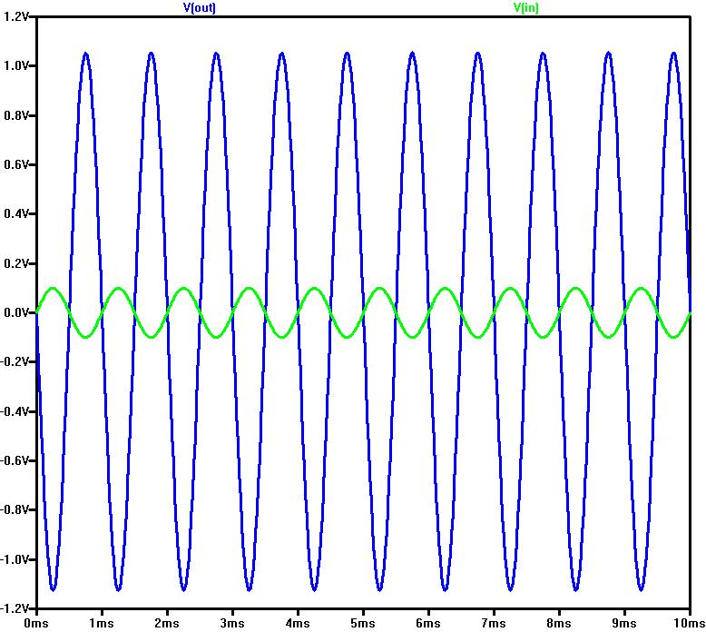
10 LTSPICE VTC PARAMETER SWEEP OF RL Add the step command to the schematic. Runs SPICE with different values of RL See appendix for Cadence PSPICE parameter sweeps IDS = 1.0mA RL= 10K 50K R1=10K VGS = 2.63V Gain of ~12V/V for 10K Rload and 1mA Page 10
11 COMMON SOURCE MOSFET AMPLIFIER +V DD Vin RS C1 RG RD + VGS - C2 RL NMOS M1 VOUT VG I D = µw Cox (Vg-Vt) 2 2L Middle of DC load line is I D = ½ Vdd/RD Page 11
12 COMMON SOURCE MOSFET AMPLIFIER I D = µw Cox (Vg-Vt) 2 2L If V DD =20V and RD=10K find Vg to give I D =1mA Middle of DC load line is I D = ½ Vdd/RD We know µ, W, L, Cox, Vt see SPICE Model at end of this document We can find Vgs to give I D =1mA For the RIT4007N7 transistor SPICE model Uo=1300 Ueff=~650 W=170u L=10u Tox=4E-8m Vt=1.4 KP=µCox = e / 4E-6 = 0.056m KP x W/L = 0.056m x 170µ/10µ = 0.952m Solve for Vg to give ID of 1mA Vg = (2 x 1m/0.952m )^ = = 2.93volts Vov = 1.53volts Page 12
13 AC EQUIVALENT CIRCUIT Vin RS RG + Vgs - gm Vgs ro RD RL + Vo - Batteries are short circuits, current sources are open circuits, capacitors are shorted. Transistor is replaced by its AC equivalent circuit. (inside dotted box) gm = d Id / d Vgs ro = d Vds / d Id at the Q point 1/slope from ID-VDS family at the Q point Page 13
14 ro, gm AND Vt FROM MEASURED ID-VDS Measured CD4007 NMOS Id vs Vds Family of Curves Extraction of Lambda, gm and Vt from measured Ids vs Vds Family of curves. ro = 1/slope = 20.9K ohms DID = 0.8ma l = slope/idsat = /5.837ma = ~0.01 ID VGS = 5.0V 4.5V 4.0V 3.5V 3.0V 2.5V 2.0V DVG = 0.5V gm = DID/DVG =0.8ma/0.5V = 1.6m S Vt = VGS where ID ~ zero = ~1.4V Page 14
15 gm is the change in current ID with change in gate voltage Vg (in excess of the threshold voltage, Vov) at the Q point ID gm= d ID / d VG slope of ID vs VG textbook gm = µcox (W/L) Vov TRANSCONDUCTANCE gm RIT4007N7 Vt=1.4 Vgs = 2.6V Vov = 1.2V gm = 1.4m gm ID gm Mobility (µ) decreases with increase in doping concentration, increase in gate and drain voltage, increase in temperature. LTSPICE Simulated Id-Vgs Curves in Saturation Region Page 15

16 SPICE CIRCUIT FOR ID vs VGS IN SATURATION Page 16

17 SPICE CIRCUIT FOR ID vs VGS NON-SATURATION Page 17
18 gm AND Vt FROM MEASURED ID-VGS Measured CD4007 NMOS Id vs Vgs Curves ID VG = VD gm = did/dvg gm = Vt = x-intercept = ~1.38V Extraction of gm from measured Ids vs Vgs in saturation region Vdg = 0 Extraction of Vt from measured Ids vs Vgs in linear region Vds = 0.1V Page 18
19 AC EQUIVALENT CIRCUIT Vin RS RG + Vgs - gm Vgs ro RL RD + Vo - µ is reduced to ½ of Uo to account for mobility degradation, Ueff = ~650 Voltage gain Vo = -gm Vgs ro//rd//rl = Vgs (ro//10k//rl) Vgs= RG/(RS+RG)Vin = Vin if RG is very big KP W/L = µ Cox (W/L) =(650)(8.85E-14)(3.9)(17)/4e-6=0.953m gm = 0.953m x Vov = 0.953m x 1.53 = 1.45mS Vo/Vin = -gm RD = -1.45m 10K = V/V (if RL is infinite and RG is big) This gm from did/dvgs using textbook equation for ID in saturation Page 19


20 SPICE FOR MOSEFET AMPLIFIER CIRCUIT Page 20
21 SUMMARY Hand Calculation SPICE IC 1mA 1mA VGS 2.93 V 2.63 V gm 1.45 ms 1.4 ms Rin Infinite infinite ro infinite 20 K ohm Vo/Vin 14.5 V/V 10.9 V/V Hand calculations from equation for ID for MOSFET in saturation. LTSPICE for CD4007 NMOSFET in common source amp circuit. Page 21
22 VIN VTC NMOS INVERTER- NMOS ENHANCEMENT LOAD +V M1 VO M2 NMOS ENHANCEMENT LOAD I M1 Vt + V - Vt 0 +V M2 is the switch and M1 is the load. The load limits the current when M2 is on. The load could be a resistor but an NMOS transistor with gate connected to the drain is smaller in size and also limits current. See the I-V characteristics. In the first quadrant the transistor approximates the resistor. However, Vout high is below VDD by the threshold voltage of M1 Cox = Cox/Area = o r/xox I 1/R V +V 0 VOUT M2 Off Vt Page 22 Gain = M2 & M1 Saturation M2 Linear W/L switch W/L load VIN I D = µw Cox (Vg-Vt) 2 2L Saturation
23 DERIVATION OF GAIN EXPRESSION VIN +VDD M1 VO M2 Assume Vout = Vin and both transistors are in saturation for the steep part of the VTC. The current in M1 is equal to the current in M2 is equal. Also assume Vt is the same for both transistors. I 2 = I 1 µw 2 Cox /2L 2 (V G -V t ) 2 = µw 1 Cox /2L 1 (V G -V t ) 2 W 2 /L 2 (V G -V t ) 2 = W 1 /L 1 (V G -V t ) 2 But, V G2 is VIN and V G1 = VO +Vt (W 2 /L 2 ) (V IN -V t ) 2 = (W 1 /L 1) (VO +Vt -V t ) 2 Gain = d VO/d V IN Gain = W2/L2 W1/L1 Gain = W/L switch W/L load Page 23

24 VTC NMOS INVERTER- NMOS ENHANCEMENT LOAD Gain = W/L switch W/L load G=9.5 G=5.5 G=2.2 Note: increasing L of the load is equivalent to increasing R of a resistor load, Vout high is Vdd Vt M1, Gain is shown. Page 24
25 VTC NMOS INVERTER- NMOS ENHANCEMENT LOAD AND V++ GATE BIAS VIN V++ +V M1 VO M2 NMOS ENHANCEMENT LOAD V++ GATE BIAS Gain = W/L switch W/L load M2 is the switch and M1 is the load. The load limits the current when M2 is on. The load could be a resistor but an NMOS transistor is smaller. M1 is always on because the gate voltage is above the supply voltage. (Vgs is always above the threshold voltage. Vout max is the supply voltage. The threshold voltage of M1 depends on source to substrate voltage for M1. Page 25

26 VTC NMOS INVERTER- NMOS ENHANCEMENT LOAD AND V++ GATE BIAS Gain = W/L switch W/L load G=2.2 G=9.5 G=5.5 Note: increasing Rochester Institute of L Technology of the load is equivalent to increasing R of a resistor load, Vout high is Vdd, Gain is shown. Page 26
27 VTC NMOS INVERTER NMOS DEPLETION LOAD VIN +V M1 VO M2 I Vt + V - I 1/R Gain = W/L switch W/L load NMOS DEPLETION LOAD Vt V M2 is the switch and M1 is the load. The load limits the current when M2 is on. In the first quadrant the transistor approximates the resistor. M1 is always on because its threshold voltage is set to zero or slightly negative by ion implant. Note: transistor M1 symbol has solid line between D and S. Page 27
28 VTC NMOS INVERTER NMOS DEPLETION LOAD * From Sub-Micron CMOS Manufacturing Classes in MicroE ~ 1um Technology.MODEL RITSUBN7D NMOS (LEVEL=7 +VERSION=3.1 CAPMOD=2 MOBMOD=1 +TOX=1.5E-8 XJ=1.84E-7 NCH=1.45E17 NSUB=5.33E16 XT=8.66E-8 +VTH0=-1.0 U0= 600 WINT=2.0E-7 LINT=1E-7 +NGATE=5E20 RSH=1082 JS=3.23E-8 JSW=3.23E-8 CJ=6.8E-4 MJ=0.5 PB=0.95 +CJSW=1.26E-10 MJSW=0.5 PBSW=0.95 PCLM=5 +CGSO=3.4E-10 CGDO=3.4E-10 CGBO=5.75E-10) Need a new SPICE model for the Depletion mode NMOS. New model name and negative VTH0. Using ion implant the VTH0 can be made negative. Page 28
29 VTC NMOS INVERTER NMOS DEPLETION LOAD D D D Gain = W/L switch W/L load G=2.2 G=9.5 G=5.5 Note: increasing L of the load is equivalent to increasing R of a resistor load, Vout high is Vdd, Gain is shown. Page 29
30 VIN +V CMOS PMOS VO NMOS CMOS - CALCULATION OF VTC +V First figure out if the transistor is sub-threshold or off, Vgs < Vth and Vgd < Vth non-saturation, Vgs > Vth and Vgd > Vth saturation region, Vgs > Vth and Vgd < Vth 0 VOUT 0 nmos off nmos sat pmos linear nmos & pmos saturation Vthn pmos sat nmos linear V-Vthp pmos off +V VIN Note: Vin Rochester = Institute Vgs, of Vout Technology = Vds, therefore Vgd = Vin-Vout Vth might be +1volt Page 30
31 CMOS INVERTER VOUT VIN VOUT +V Q point +V Idd Slope = Gain VIN VO CMOS 0 0 +V VIN Vinv Page 31
32 BIASING AT VIN = VOUT V+ Vin RG pmos nmos Vout Since no DC current flows into the gate for either MOSFET the voltage across RG is zero. DC Vin=Vout and is the Q point. RG can be large but not infinite. Page 32
33 Vin RS Rin AC EQUIVALENT CIRCUIT + Vgs - RG gm n Vgs gm p Vgs ro n ro p Rout Batteries are short circuits, current sources are open circuits, capacitors are shorted. Transistor is replaced by its AC equivalent circuit. NMOS and PMOS are in parallel If RG and RL is large the gain is Vo/Vin= ~(gm n +gm p ) (ro n //ro p ) RL + Vo - Example: Vo/Vin = (1.5m+1.5m)(20K//20K) =30 V/V Page 33


34 CMOS AMPLIFIER BIASED AT VIN=VOUT Page 34
35 COMPARISON OF 10u, 1u AND 100n CMOS INVERTERS VDD = 5 volts VDD = 3.3 volts VDD = 2.5 volts Imax=5.4mA Imax=100uA Imax=21uA Gain=-90 Gain=-17 Gain=-6 RITALDN3/RITALDP3 L=10u W=880u L=10u W=880u RITSUBN7/RITSUBP7 Ln=1u Wn=2u Lp=1u Wp=2u EECMOSN/EECMOSP Ln=180n Wp=200n Ln=180n Wp=200n Page 35
36 MULTI-STAGE CAPACITOR COUPLED MOS AMP +V DD +V DD Vin RS C1 RG RD + VGS - C2 M1 RG RD + VGS - M2 C3 VOUT RL VG VG Rs Ro1 Ro2 Rin1 + AvVin1 + Rin2 AvVin Vin1 - Vin2 - vs - - RL + - vo Stage 1 Stage 2 Page 36
37 OTHER CONFIGURATIONS Common Gate Biasing Schemes still working on these Page 37
38 REFERNCES 1. Sedra and Smith, Microelectronic Circuits, Sixth Edition, Chapter Dr. Fuller s Lecture Notes, Page 38
39 HOMEWORK MOS AMPLIFIERS 1. Derive the equation gm = µcox (W/L) Vov starting from the equation for Id in the saturation region. 2. Design a NMOS amplifier with NMOS enhancement load to give a gain of 10V/V or more. 3. How can you get higher voltage gain for the CMOS Amplifier shown in the SPICE simulation in the lecture notes? Page 39
40 SPICE MODELS FOR CD4007 MOSFETS *SPICE MODELS FOR RIT DEVICES - DR. LYNN FULLER *LOCATION DR.FULLER'S WEBPAGE - * *Used in Electronics II for CD4007 inverter chip *Note: Properties L=10u W=170u Ad=8500p As=8500p Pd=440u Ps=440u NRD=0.1 NRS=0.1.MODEL RIT4007N7 NMOS (LEVEL=7 +VERSION=3.1 CAPMOD=2 MOBMOD=1 +TOX=4E-8 XJ=2.9E-7 NCH=4E15 NSUB=5.33E15 XT=8.66E-8 +VTH0=1.4 U0= 1300 WINT=2.0E-7 LINT=1E-7 +NGATE=5E20 RSH=300 JS=3.23E-8 JSW=3.23E-8 CJ=6.8E-8 MJ=0.5 PB=0.95 +CJSW=1.26E-10 MJSW=0.5 PBSW=0.95 PCLM=5 +CGSO=3.4E-10 CGDO=3.4E-10 CGBO=5.75E-10) * *Used in Electronics II for CD4007 inverter chip *Note: Properties L=10u W=360u Ad=18000p As=18000p Pd=820u Ps=820u NRS=O.54 NRD=0.54.MODEL RIT4007P7 PMOS (LEVEL=7 +VERSION=3.1 CAPMOD=2 MOBMOD=1 +TOX=5E-8 XJ=2.26E-7 NCH=1E15 NSUB=8E14 XT=8.66E-8 +VTH0=-1.65 U0= 400 WINT=1.0E-6 LINT=1E-6 +NGATE=5E20 RSH=1347 JS=3.51E-8 JSW=3.51E-8 CJ=5.28E-8 MJ=0.5 PB=0.94 +CJSW=1.19E-10 MJSW=0.5 PBSW=0.94 pclm=5 +CGSO=4.5E-10 CGDO=4.5E-10 CGBO=5.75E-10) Page 40
41 SPICE MODELS FOR MOSFETS * From Sub-Micron CMOS Manufacturing Classes in MicroE ~ 1um Technology.MODEL RITSUBN7 NMOS (LEVEL=7 +VERSION=3.1 CAPMOD=2 MOBMOD=1 +TOX=1.5E-8 XJ=1.84E-7 NCH=1.45E17 NSUB=5.33E16 XT=8.66E-8 +VTH0=1.0 U0= 600 WINT=2.0E-7 LINT=1E-7 +NGATE=5E20 RSH=1082 JS=3.23E-8 JSW=3.23E-8 CJ=6.8E-4 MJ=0.5 PB=0.95 +CJSW=1.26E-10 MJSW=0.5 PBSW=0.95 PCLM=5 +CGSO=3.4E-10 CGDO=3.4E-10 CGBO=5.75E-10) * *From Sub-Micron CMOS Manufacturing Classes in MicroE ~ 1um Technology.MODEL RITSUBP7 PMOS (LEVEL=7 +VERSION=3.1 CAPMOD=2 MOBMOD=1 +TOX=1.5E-8 XJ=2.26E-7 NCH=7.12E16 NSUB=3.16E16 XT=8.66E-8 +VTH0=-1.0 U0= WINT=2.0E-7 LINT=2.26E-7 +NGATE=5E20 RSH=1347 JS=3.51E-8 JSW=3.51E-8 CJ=5.28E-4 MJ=0.5 PB=0.94 +CJSW=1.19E-10 MJSW=0.5 PBSW=0.94 +CGSO=4.5E-10 CGDO=4.5E-10 CGBO=5.75E-10) Page 41
42 SPICE MODELS FOR MOSFETS * LTSPICE uses Level=8 * From Electronics II EEEE482 FOR ~100nm Technology.model EECMOSN NMOS (LEVEL=8 +VERSION=3.1 CAPMOD=2 MOBMOD=1 +TOX=5E-9 XJ=1.84E-7 NCH=1E17 NSUB=5E16 XT=5E-8 +VTH0=0.4 U0= 200 WINT=1E-8 LINT=1E-8 +NGATE=5E20 RSH=1000 JS=3.23E-8 JSW=3.23E-8 CJ=6.8E-4 MJ=0.5 PB=0.95 +CJSW=1.26E-10 MJSW=0.5 PBSW=0.95 PCLM=5 +CGSO=3.4E-10 CGDO=3.4E-10 CGBO=5.75E-10) * * LTSPICE uses Level=8 * From Electronics II EEEE482 FOR ~100nm Technology.model EECMOSP PMOS (LEVEL=8 +TOX=5E-9 XJ=0.05E-6 NCH=1E17 NSUB=5E16 XT=5E-8 +VTH0=-0.4 U0= 100 WINT=1E-8 LINT=1E-8 +NGATE=5E20 RSH=1000 JS=3.51E-8 JSW=3.51E-8 CJ=5.28E-4 MJ=0.5 PB=0.94 +CJSW=1.19E-10 MJSW=0.5 PBSW=0.94 PCLM=5 +CGSO=4.5E-10 CGDO=4.5E-10 CGBO=5.75E-10) * Page 42


43 APPENDIX - CADENCE PARAMETER SWEEPS Select Parameters: from the special library and put on schematic. Then double click it. Select New Property. Give a Name and starting Value in Add New Property dialog box shown below. Apply. Page 43

44 APPENDIX - CADENCE PARAMETER SWEEPS Return to schematic and change the value of the resistor to {Rval} Including curly brackets Where this is the new property name given in the attribute editor The primary sweep is for V1, zero to 5 volts in small steps. Parameter sweep can be a list of values as shown. Page 44
45 APPENDIX - CADENCE PARAMETER SWEEPS 5.0V V(output) 4.0V R=1K 3.0V 2.0V 50K 10K 1.0V 0V 0V 1.0V 2.0V 3.0V 4.0V 5.0V V(output) V_V1 Vin Page 45
Transfer Gate and Dynamic Logic Dr. Lynn Fuller Webpage:
 ROCHESTER INSTITUTE OF TECHNOLOGY MICROELECTRONIC ENGINEERING Transfer Gate and Dynamic Logic Dr. Lynn Fuller Webpage: http://people.rit.edu/lffeee 82 Lomb Memorial Drive Rochester, NY 14623-5604 Tel (585)
Combinatorial and Sequential CMOS Circuits Dr. Lynn Fuller Webpage:
 ROCHESTER INSTITUTE OF TECHNOLOGY MICROELECTRONIC ENGINEERING Combinatorial and Sequential CMOS Circuits Webpage: http://people.rit.edu/lffeee 82 Lomb Memorial Drive Rochester, NY 14623-5604 Tel (585)
High Speed Logic Circuits Dr. Lynn Fuller Webpage:
 ROCHESTER INSTITUTE OF TECHNOLOGY MICROELECTRONIC ENGINEERING Circuits Webpage: http://people.rit.edu/lffeee 82 Lomb Memorial Drive Rochester, NY 14623-5604 Tel (585) 475-2035 Fax (585) 475-5041 Email:
MOSFET Internal Capacitance Dr. Lynn Fuller Webpage:
 ROCHESTER INSTITUTE OF TECHNOLOGY MICROELECTRONIC ENGINEERING Dr. Lynn Fuller Webpage: http://people.rit.edu/lffeee 82 Lomb Memorial Drive Rochester, NY 14623-5604 Email: Lynn.Fuller@rit.edu Department
Lecture 13 MOSFET as an amplifier with an introduction to MOSFET small-signal model and small-signal schematics. Lena Peterson
 Lecture 13 MOSFET as an amplifier with an introduction to MOSFET small-signal model and small-signal schematics Lena Peterson 2015-10-13 Outline (1) Why is the CMOS inverter gain not infinite? Large-signal
ECE 523/421 - Analog Electronics University of New Mexico Solutions Homework 3
 ECE 523/42 - Analog Electronics University of New Mexico Solutions Homework 3 Problem 7.90 Show that when ro is taken into account, the voltage gain of the source follower becomes G v v o v sig R L r o
Low Power CMOS Dr. Lynn Fuller Webpage:
 ROCHESTER INSTITUTE OF TECHNOLOGY MICROELECTRONIC ENGINEERING Dr. Lynn Fuller Webpage: http://people.rit.edu/lffeee 82 Lomb Memorial Drive Rochester, NY 14623-5604 Email: Lynn.Fuller@rit.edu Department
ECEN474/704: (Analog) VLSI Circuit Design Spring 2018
 VLSI Circuit Design Spring 2018") ECEN474/704: (Analog) VLSI Circuit Design Spring 2018 Lecture 4: MOS ransistor Modeling Sam Palermo Analog & Mixed-Signal Center exas A&M University Agenda MOS ransistor Modeling MOS Spice Models MOS High-Order
ECEN474/704: (Analog) VLSI Circuit Design Spring 2018 Lecture 4: MOS ransistor Modeling Sam Palermo Analog & Mixed-Signal Center exas A&M University Agenda MOS ransistor Modeling MOS Spice Models MOS High-Order
Digital Integrated Circuits
 Chapter 6 The CMOS Inverter 1 Contents Introduction (MOST models) 0, 1 st, 2 nd order The CMOS inverter : The static behavior: o DC transfer characteristics, o Short-circuit current The CMOS inverter :
1. (50 points, BJT curves & equivalent) For the 2N3904 =(npn) and the 2N3906 =(pnp)
 For the 2N3904 =(npn) and the 2N3906 =(pnp)") HW 3 1. (50 points, BJT curves & equivalent) For the 2N3904 =(npn) and the 2N3906 =(pnp) a) Obtain in Spice the transistor curves given on the course web page except do in separate plots, one for the npn
HW 3 1. (50 points, BJT curves & equivalent) For the 2N3904 =(npn) and the 2N3906 =(pnp) a) Obtain in Spice the transistor curves given on the course web page except do in separate plots, one for the npn
ECE 342 Electronic Circuits. 3. MOS Transistors
 ECE 342 Electronic Circuits 3. MOS Transistors Jose E. Schutt-Aine Electrical & Computer Engineering University of Illinois jschutt@emlab.uiuc.edu 1 NMOS Transistor Typically L = 0.1 to 3 m, W = 0.2 to
Today s lecture. EE141- Spring 2003 Lecture 4. Design Rules CMOS Inverter MOS Transistor Model
 - Spring 003 Lecture 4 Design Rules CMOS Inverter MOS Transistor Model Today s lecture Design Rules The CMOS inverter at a glance An MOS transistor model for manual analysis Important! Labs start next
(S&S ) PMOS: holes flow from Source to Drain. from Source to Drain. W.-Y. Choi. Electronic Circuits 2 (09/1)
 PMOS: holes flow from Source to Drain. from Source to Drain. W.-Y. Choi. Electronic Circuits 2 (09/1)") (S&S 4.1 4.3) NMOS: electrons flow from Source to Drain PMOS: holes flow from Source to Drain In cut-off ( v < V ), i = 0 GS t D NMOS I-V Characteristics In triode, ( v > V but v v v ) GS t DS GS T W 1
(S&S 4.1 4.3) NMOS: electrons flow from Source to Drain PMOS: holes flow from Source to Drain In cut-off ( v < V ), i = 0 GS t D NMOS I-V Characteristics In triode, ( v > V but v v v ) GS t DS GS T W 1
ECE 342 Electronic Circuits. Lecture 6 MOS Transistors
 ECE 342 Electronic Circuits Lecture 6 MOS Transistors Jose E. Schutt-Aine Electrical & Computer Engineering University of Illinois jesa@illinois.edu 1 NMOS Transistor Typically L = 0.1 to 3 m, W = 0.2
Study of MOSFET circuit
 ECE 570 Computer Aided Engineering for Integrated Circuits IC 752 - E Simulation Assignment No. 3 - Due: Oct. 30 (Th.), 2003 Study of MOSFET circuit Simulate the basic circuit of CMOS shift register shown
Lecture 4: CMOS Transistor Theory
 Introduction to CMOS VLSI Design Lecture 4: CMOS Transistor Theory David Harris, Harvey Mudd College Kartik Mohanram and Steven Levitan University of Pittsburgh Outline q Introduction q MOS Capacitor q
MOS Transistor Properties Review
 MOS Transistor Properties Review 1 VLSI Chip Manufacturing Process Photolithography: transfer of mask patterns to the chip Diffusion or ion implantation: selective doping of Si substrate Oxidation: SiO
Device Models (PN Diode, MOSFET )
") Device Models (PN Diode, MOSFET ) Instructor: Steven P. Levitan steve@ece.pitt.edu TA: Gayatri Mehta, José Martínez Book: Digital Integrated Circuits: A Design Perspective; Jan Rabaey Lab Notes: Handed
Device Models (PN Diode, MOSFET ) Instructor: Steven P. Levitan steve@ece.pitt.edu TA: Gayatri Mehta, José Martínez Book: Digital Integrated Circuits: A Design Perspective; Jan Rabaey Lab Notes: Handed
CMOS INVERTER. Last Lecture. Metrics for qualifying digital circuits. »Cost» Reliability» Speed (delay)»performance
»performance") CMOS INVERTER Last Lecture Metrics for qualifying digital circuits»cost» Reliability» Speed (delay)»performance 1 Today s lecture The CMOS inverter at a glance An MOS transistor model for manual analysis
CMOS INVERTER Last Lecture Metrics for qualifying digital circuits»cost» Reliability» Speed (delay)»performance 1 Today s lecture The CMOS inverter at a glance An MOS transistor model for manual analysis
ECE 546 Lecture 10 MOS Transistors
 ECE 546 Lecture 10 MOS Transistors Spring 2018 Jose E. Schutt-Aine Electrical & Computer Engineering University of Illinois jesa@illinois.edu NMOS Transistor NMOS Transistor N-Channel MOSFET Built on p-type
Fig. 1 CMOS Transistor Circuits (a) Inverter Out = NOT In, (b) NOR-gate C = NOT (A or B)
 Inverter Out = NOT In, (b) NOR-gate C = NOT (A or B)") 1 Introduction to Transistor-Level Logic Circuits 1 By Prawat Nagvajara At the transistor level of logic circuits, transistors operate as switches with the logic variables controlling the open or closed
1 Introduction to Transistor-Level Logic Circuits 1 By Prawat Nagvajara At the transistor level of logic circuits, transistors operate as switches with the logic variables controlling the open or closed
CHAPTER 3: TRANSISTOR MOSFET DR. PHAM NGUYEN THANH LOAN. Hà Nội, 9/24/2012
 1 CHAPTER 3: TRANSISTOR MOSFET DR. PHAM NGUYEN THANH LOAN Hà Nội, 9/24/2012 Chapter 3: MOSFET 2 Introduction Classifications JFET D-FET (Depletion MOS) MOSFET (Enhancement E-FET) DC biasing Small signal
EE105 - Fall 2005 Microelectronic Devices and Circuits
 EE105 - Fall 005 Microelectronic Devices and Circuits ecture 7 MOS Transistor Announcements Homework 3, due today Homework 4 due next week ab this week Reading: Chapter 4 1 ecture Material ast lecture
EE 560 MOS TRANSISTOR THEORY PART 2. Kenneth R. Laker, University of Pennsylvania
 1 EE 560 MOS TRANSISTOR THEORY PART nmos TRANSISTOR IN LINEAR REGION V S = 0 V G > V T0 channel SiO V D = small 4 C GC C BC substrate depletion region or bulk B p nmos TRANSISTOR AT EDGE OF SATURATION
UNIVERSITY OF CALIFORNIA College of Engineering Department of Electrical Engineering and Computer Sciences PROBLEM SET #3 (SOLUTION)
") UNIVERSITY OF CALIFORNIA College of Engineering Department of Electrical Engineering and Computer Sciences R. W. Brodersen EECS 140 Fall 2004 PROBLEM SET #3 (SOLUTION) 3) In the above circuit, use V DD
UNIVERSITY OF CALIFORNIA College of Engineering Department of Electrical Engineering and Computer Sciences R. W. Brodersen EECS 140 Fall 2004 PROBLEM SET #3 (SOLUTION) 3) In the above circuit, use V DD
CMPEN 411 VLSI Digital Circuits. Lecture 04: CMOS Inverter (static view)
") CMPEN 411 VLSI Digital Circuits Lecture 04: CMOS Inverter (static view) Kyusun Choi [Adapted from Rabaey s Digital Integrated Circuits, Second Edition, 2003 J. Rabaey, A. Chandrakasan, B. Nikolic] CMPEN
CMPEN 411 VLSI Digital Circuits Lecture 04: CMOS Inverter (static view) Kyusun Choi [Adapted from Rabaey s Digital Integrated Circuits, Second Edition, 2003 J. Rabaey, A. Chandrakasan, B. Nikolic] CMPEN
CMPEN 411 VLSI Digital Circuits. Lecture 03: MOS Transistor
 CMPEN 411 VLSI Digital Circuits Lecture 03: MOS Transistor Kyusun Choi [Adapted from Rabaey s Digital Integrated Circuits, Second Edition, 2003 J. Rabaey, A. Chandrakasan, B. Nikolic] CMPEN 411 L03 S.1
EE 330 Homework 5 Spring 2017 (This assignment will not be collected or graded)
") EE 330 Homework 5 Spring 2017 (This assignment will not be collected or graded) Assume the CMOS process is characterized by model parameters V TH =1V and µc OX =100µA/V 2. If any other model parameters
EE 330 Homework 5 Spring 2017 (This assignment will not be collected or graded) Assume the CMOS process is characterized by model parameters V TH =1V and µc OX =100µA/V 2. If any other model parameters
EE105 - Fall 2006 Microelectronic Devices and Circuits
 EE105 - Fall 2006 Microelectronic Devices and Circuits Prof. Jan M. Rabaey (jan@eecs) Lecture 7: MOS Transistor Some Administrative Issues Lab 2 this week Hw 2 due on We Hw 3 will be posted same day MIDTERM
The Physical Structure (NMOS)
") The Physical Structure (NMOS) Al SiO2 Field Oxide Gate oxide S n+ Polysilicon Gate Al SiO2 SiO2 D n+ L channel P Substrate Field Oxide contact Metal (S) n+ (G) L W n+ (D) Poly 1 Transistor Resistance Two
The Physical Structure (NMOS) Al SiO2 Field Oxide Gate oxide S n+ Polysilicon Gate Al SiO2 SiO2 D n+ L channel P Substrate Field Oxide contact Metal (S) n+ (G) L W n+ (D) Poly 1 Transistor Resistance Two
MOS Transistors Models
 MOS Transistors Models Andreas G. Andreou Pedro Julian Electrical and Computer Engineering Johns Hopkins University http://andreoulab.net The MOS transistor Levels of Abstraction- Model Equations If V
EE 330 Lecture 17. MOSFET Modeling CMOS Process Flow
 EE 330 Lecture 17 MOSFET Modeling CMOS Process Flow Review from Last Lecture Limitations of Existing Models V DD V OUT V OUT V DD?? V IN V OUT V IN V IN V DD Switch-Level Models V DD Simple square-law
1/13/12 V DS. I d V GS. C ox ( = f (V GS ,V DS ,V SB = I D. + i d + I ΔV + I ΔV BS V BS. 19 January 2012
 /3/ 9 January 0 Study the linear model of MOS transistor around an operating point." MOS in saturation: V GS >V th and V S >V GS -V th " VGS vi - I d = I i d VS I d = µ n ( L V V γ Φ V Φ GS th0 F SB F
The Devices. Devices
 The The MOS Transistor Gate Oxyde Gate Source n+ Polysilicon Drain n+ Field-Oxyde (SiO 2 ) p-substrate p+ stopper Bulk Contact CROSS-SECTION of NMOS Transistor Cross-Section of CMOS Technology MOS transistors
MOS Transistor Theory
 MOS Transistor Theory So far, we have viewed a MOS transistor as an ideal switch (digital operation) Reality: less than ideal EE 261 Krish Chakrabarty 1 Introduction So far, we have treated transistors
MOS Transistor I-V Characteristics and Parasitics
 ECEN454 Digital Integrated Circuit Design MOS Transistor I-V Characteristics and Parasitics ECEN 454 Facts about Transistors So far, we have treated transistors as ideal switches An ON transistor passes
EE 330 Lecture 16. MOSFET Modeling CMOS Process Flow
 EE 330 Lecture 16 MOSFET Modeling CMOS Process Flow Model Extensions 300 Id 250 200 150 100 50 300 0 0 1 2 3 4 5 Vds Existing Model 250 200 Id 150 100 50 Slope is not 0 0 0 1 2 3 4 Actual Device Vds Model
Integrated Circuit Design: OTA in 0.5µm Technology
 Integrated Circuit Design: OTA in 0.5µm Technology Omar X. Avelar, Omar de la Mora & Diego I. Romero INTEGRATED CIRCUITS DESIGN (ESI108A) Instituto Tecnológico y de Estudios Superiores de Occidente (ITESO)
ECEN474/704: (Analog) VLSI Circuit Design Spring 2018
 VLSI Circuit Design Spring 2018") ECEN474/704: (Analog) SI Circuit Design Spring 2018 ecture 2: MOS ransistor Modeling Sam Palermo Analog & Mixed-Signal Center exas A&M University Announcements If you haven t already, turn in your 0.18um
ECEN474/704: (Analog) SI Circuit Design Spring 2018 ecture 2: MOS ransistor Modeling Sam Palermo Analog & Mixed-Signal Center exas A&M University Announcements If you haven t already, turn in your 0.18um
The Devices. Digital Integrated Circuits A Design Perspective. Jan M. Rabaey Anantha Chandrakasan Borivoje Nikolic. July 30, 2002
 Digital Integrated Circuits A Design Perspective Jan M. Rabaey Anantha Chandrakasan Borivoje Nikolic The Devices July 30, 2002 Goal of this chapter Present intuitive understanding of device operation Introduction
MOS Transistor Theory
 CHAPTER 3 MOS Transistor Theory Outline 2 1. Introduction 2. Ideal I-V Characteristics 3. Nonideal I-V Effects 4. C-V Characteristics 5. DC Transfer Characteristics 6. Switch-level RC Delay Models MOS
Lecture 3: CMOS Transistor Theory
 Lecture 3: CMOS Transistor Theory Outline Introduction MOS Capacitor nmos I-V Characteristics pmos I-V Characteristics Gate and Diffusion Capacitance 2 Introduction So far, we have treated transistors
ECE 415/515 ANALOG INTEGRATED CIRCUIT DESIGN
 ECE 415/515 ANALOG INTEGRATED CIRCUIT DESIGN CMOS PROCESS CHARACTERIZATION VISHAL SAXENA VSAXENA@UIDAHO.EDU Vishal Saxena DESIGN PARAMETERS Analog circuit designers care about: Open-loop Gain: g m r o
Chapter 4 Field-Effect Transistors
 Chapter 4 Field-Effect Transistors Microelectronic Circuit Design Richard C. Jaeger Travis N. Blalock 5/5/11 Chap 4-1 Chapter Goals Describe operation of MOSFETs. Define FET characteristics in operation
CMOS Inverter (static view)
") Review: Design Abstraction Levels SYSTEM CMOS Inverter (static view) + MODULE GATE [Adapted from Chapter 5. 5.3 CIRCUIT of G DEVICE Rabaey s Digital Integrated Circuits,, J. Rabaey et al.] S D Review:
Review: Design Abstraction Levels SYSTEM CMOS Inverter (static view) + MODULE GATE [Adapted from Chapter 5. 5.3 CIRCUIT of G DEVICE Rabaey s Digital Integrated Circuits,, J. Rabaey et al.] S D Review:
Design of Analog Integrated Circuits
 Design of Analog Integrated Circuits Chapter 11: Introduction to Switched- Capacitor Circuits Textbook Chapter 13 13.1 General Considerations 13.2 Sampling Switches 13.3 Switched-Capacitor Amplifiers 13.4
Digital Integrated Circuits A Design Perspective. Jan M. Rabaey Anantha Chandrakasan Borivoje Nikolic. The Devices. July 30, Devices.
 Digital Integrated Circuits A Design Perspective Jan M. Rabaey Anantha Chandrakasan Borivoje Nikolic The July 30, 2002 1 Goal of this chapter Present intuitive understanding of device operation Introduction
Lecture 04 Review of MOSFET
 ECE 541/ME 541 Microelectronic Fabrication Techniques Lecture 04 Review of MOSFET Zheng Yang (ERF 3017, email: yangzhen@uic.edu) What is a Transistor? A Switch! An MOS Transistor V GS V T V GS S Ron D
Lecture 15: MOS Transistor models: Body effects, SPICE models. Context. In the last lecture, we discussed the modes of operation of a MOS FET:
 Lecture 15: MOS Transistor models: Body effects, SPICE models Context In the last lecture, we discussed the modes of operation of a MOS FET: oltage controlled resistor model I- curve (Square-Law Model)
Lecture 12: MOSFET Devices
 Lecture 12: MOSFET Devices Gu-Yeon Wei Division of Engineering and Applied Sciences Harvard University guyeon@eecs.harvard.edu Wei 1 Overview Reading S&S: Chapter 5.1~5.4 Supplemental Reading Background
Microelectronics Main CMOS design rules & basic circuits
 GBM8320 Dispositifs médicaux intelligents Microelectronics Main CMOS design rules & basic circuits Mohamad Sawan et al. Laboratoire de neurotechnologies Polystim mohamad.sawan@polymtl.ca M5418 6 & 7 September
Microelectronics Part 1: Main CMOS circuits design rules
 GBM8320 Dispositifs Médicaux telligents Microelectronics Part 1: Main CMOS circuits design rules Mohamad Sawan et al. Laboratoire de neurotechnologies Polystim! http://www.cours.polymtl.ca/gbm8320/! med-amine.miled@polymtl.ca!
Chapter 2 CMOS Transistor Theory. Jin-Fu Li Department of Electrical Engineering National Central University Jungli, Taiwan
 Chapter 2 CMOS Transistor Theory Jin-Fu Li Department of Electrical Engineering National Central University Jungli, Taiwan Outline Introduction MOS Device Design Equation Pass Transistor Jin-Fu Li, EE,
EE105 Fall 2014 Microelectronic Devices and Circuits. NMOS Transistor Capacitances: Saturation Region
 EE105 Fall 014 Microelectronic Devices and Circuits Prof. Ming C. Wu wu@eecs.berkeley.edu 511 Sutardja Dai Hall (SDH) 1 NMOS Transistor Capacitances: Saturation Region Drain no longer connected to channel
EE 330 Lecture 16. Devices in Semiconductor Processes. MOS Transistors
 EE 330 Lecture 16 Devices in Semiconductor Processes MOS Transistors Review from Last Time Model Summary I D I V DS V S I B V BS = 0 0 VS VT W VDS ID = μcox VS VT VDS VS V VDS VS VT L T < W μc ( V V )
EE 330 Homework 5 Fall 2018 (This assignment is due Wednesday Sept 19 at 12:00 noon)
") EE 330 Homework 5 Fall 2018 (This assignment is due Wednesday Sept 19 at 12:00 noon) Assume the CMOS process is characterized by model parameters VTH=1V and µcox=100µa/v 2. If any other model parameters
EE 330 Homework 5 Fall 2018 (This assignment is due Wednesday Sept 19 at 12:00 noon) Assume the CMOS process is characterized by model parameters VTH=1V and µcox=100µa/v 2. If any other model parameters
EE105 - Fall 2006 Microelectronic Devices and Circuits. Some Administrative Issues
 EE105 - Fall 006 Microelectronic evices and Circuits Prof. Jan M. Rabaey (jan@eecs Lecture 8: MOS Small Signal Model Some Administrative Issues REIEW Session Next Week Tu Sept 6 6:00-7:30pm; 060 alley
The Devices: MOS Transistors
 The Devices: MOS Transistors References: Semiconductor Device Fundamentals, R. F. Pierret, Addison-Wesley Digital Integrated Circuits: A Design Perspective, J. Rabaey et.al. Prentice Hall NMOS Transistor
Device Models (PN Diode, MOSFET )
") Device Models (PN Diode, MOSFET ) Instructor: Steven P. Levitan steve@ece.pitt.edu TA: Gayatri Mehta, José Martínez Book: Digital Integrated Circuits: A Design Perspective; Jan Rabaey Lab Notes: Handed
Device Models (PN Diode, MOSFET ) Instructor: Steven P. Levitan steve@ece.pitt.edu TA: Gayatri Mehta, José Martínez Book: Digital Integrated Circuits: A Design Perspective; Jan Rabaey Lab Notes: Handed
Lecture 11: MOS Transistor
 Lecture 11: MOS Transistor Prof. Niknejad Lecture Outline Review: MOS Capacitors Regions MOS Capacitors (3.8 3.9) CV Curve Threshold Voltage MOS Transistors (4.1 4.3): Overview Cross-section and layout
Integrated Circuits & Systems
 Federal University of Santa Catarina Center for Technology Computer Science & Electronics Engineering Integrated Circuits & Systems INE 5442 Lecture 10 MOSFET part 1 guntzel@inf.ufsc.br ual-well Trench-Isolated
MOSFET: Introduction
 E&CE 437 Integrated VLSI Systems MOS Transistor 1 of 30 MOSFET: Introduction Metal oxide semiconductor field effect transistor (MOSFET) or MOS is widely used for implementing digital designs Its major
EEE 421 VLSI Circuits
 EEE 421 CMOS Properties Full rail-to-rail swing high noise margins» Logic levels not dependent upon the relative device sizes transistors can be minimum size ratioless Always a path to V dd or GND in steady
ECE 546 Lecture 11 MOS Amplifiers
 ECE 546 Lecture MOS Amplifiers Spring 208 Jose E. Schutt-Aine Electrical & Computer Engineering University of Illinois jesa@illinois.edu ECE 546 Jose Schutt Aine Amplifiers Definitions Used to increase
PRESIDENCY UNIVERSITY DEPARTMENT OF ELECTRICAL AND COMPUTER ENGINEERING EE 310: VLSI System Laboratory. Contents
 PRESIDENCY UNIVERSITY DEPARTMENT OF ELECTRICAL AND COMPUTER ENGINEERING EE 310: VLSI System Laboratory Contents Experiment No Name of The Experiments. Page Experiment-1 INTRODUCTION TO CIRCUIT SIMULATION
Important! EE141- Fall 2002 Lecture 5. CMOS Inverter MOS Transistor Model
 - Fall 00 Lecture 5 CMO Inverter MO Transistor Model Important! Lab 3 this week You must show up in one of the lab sessions this week If you don t show up you will be dropped from the class» Unless you
P. R. Nelson 1 ECE418 - VLSI. Midterm Exam. Solutions
 P. R. Nelson 1 ECE418 - VLSI Midterm Exam Solutions 1. (8 points) Draw the cross-section view for A-A. The cross-section view is as shown below.. ( points) Can you tell which of the metal1 regions is the
SECTION: Circle one: Alam Lundstrom. ECE 305 Exam 5 SOLUTIONS: Spring 2016 April 18, 2016 M. A. Alam and M.S. Lundstrom Purdue University
 NAME: PUID: SECTION: Circle one: Alam Lundstrom ECE 305 Exam 5 SOLUTIONS: April 18, 2016 M A Alam and MS Lundstrom Purdue University This is a closed book exam You may use a calculator and the formula
Practice 3: Semiconductors
 Practice 3: Semiconductors Digital Electronic Circuits Semester A 2012 VLSI Fabrication Process VLSI Very Large Scale Integration The ability to fabricate many devices on a single substrate within a given
ECE 342 Solid State Devices & Circuits 4. CMOS
 ECE 34 Solid State Devices & Circuits 4. CMOS Jose E. Schutt-Aine Electrical & Computer Engineering University of Illinois jschutt@emlab.uiuc.edu ECE 34 Jose Schutt Aine 1 Digital Circuits V IH : Input
EECS 105: FALL 06 FINAL
 University of California College of Engineering Department of Electrical Engineering and Computer Sciences Jan M. Rabaey TuTh 2-3:30 Wednesday December 13, 12:30-3:30pm EECS 105: FALL 06 FINAL NAME Last
ESE 570 MOS TRANSISTOR THEORY Part 2
 ESE 570 MOS TRANSISTOR THEORY Part 2 GCA (gradual channel approximation) MOS Transistor Model Strong Inversion Operation CMOS = NMOS + PMOS 2 TwoTerminal MOS Capacitor > nmos Transistor VGS
DC and Transient Responses (i.e. delay) (some comments on power too!)
 (some comments on power too!)") DC and Transient Responses (i.e. delay) (some comments on power too!) Michael Niemier (Some slides based on lecture notes by David Harris) 1 Lecture 02 - CMOS Transistor Theory & the Effects of Scaling
DC and Transient Responses (i.e. delay) (some comments on power too!) Michael Niemier (Some slides based on lecture notes by David Harris) 1 Lecture 02 - CMOS Transistor Theory & the Effects of Scaling
MOS Transistors. Prof. Krishna Saraswat. Department of Electrical Engineering Stanford University Stanford, CA
 MOS Transistors Prof. Krishna Saraswat Department of Electrical Engineering S Stanford, CA 94305 saraswat@stanford.edu 1 1930: Patent on the Field-Effect Transistor! Julius Lilienfeld filed a patent describing
Fundamentals of the Metal Oxide Semiconductor Field-Effect Transistor
 Triode Working FET Fundamentals of the Metal Oxide Semiconductor Field-Effect Transistor The characteristics of energy bands as a function of applied voltage. Surface inversion. The expression for the
Chapter 13 Small-Signal Modeling and Linear Amplification
 Chapter 13 Small-Signal Modeling and Linear Amplification Microelectronic Circuit Design Richard C. Jaeger Travis N. Blalock 1/4/12 Chap 13-1 Chapter Goals Understanding of concepts related to: Transistors
6.012 Electronic Devices and Circuits Spring 2005
 6.012 Electronic Devices and Circuits Spring 2005 May 16, 2005 Final Exam (200 points) -OPEN BOOK- Problem NAME RECITATION TIME 1 2 3 4 5 Total General guidelines (please read carefully before starting):
Field-Effect (FET) transistors
 transistors") Field-Effect (FET) transistors References: Barbow (Chapter 8), Rizzoni (chapters 8 & 9) In a field-effect transistor (FET), the width of a conducting channel in a semiconductor and, therefore, its current-carrying
Field-Effect (FET) transistors References: Barbow (Chapter 8), Rizzoni (chapters 8 & 9) In a field-effect transistor (FET), the width of a conducting channel in a semiconductor and, therefore, its current-carrying
University of Pennsylvania Department of Electrical Engineering. ESE 570 Midterm Exam March 14, 2013 FORMULAS AND DATA
 University of Pennsylvania Department of Electrical Engineering ESE 570 Midterm Exam March 4, 03 FORMULAS AND DATA. PHYSICAL CONSTANTS: n i = intrinsic concentration undoped) silicon =.45 x 0 0 cm -3 @
Lecture 5: DC & Transient Response
 Lecture 5: DC & Transient Response Outline q Pass Transistors q DC Response q Logic Levels and Noise Margins q Transient Response q RC Delay Models q Delay Estimation 2 Activity 1) If the width of a transistor
Chapter 20. Current Mirrors. Basics. Cascoding. Biasing Circuits. Baker Ch. 20 Current Mirrors. Introduction to VLSI
 Chapter 20 Current Mirrors Basics Long Channel Matching Biasing Short Channel Temperature Subthreshold Cascoding Simple Low Voltage, Wide Swing Wide Swing, Short Channel Regulated Drain Biasing Circuits
EE 330 Lecture 16. MOS Device Modeling p-channel n-channel comparisons Model consistency and relationships CMOS Process Flow
 EE 330 Lecture 16 MOS Device Modeling p-channel n-channel comparisons Model consistency and relationships CMOS Process Flow Review from Last Time Operation Regions by Applications Id I D 300 250 200 150
UNIVERSITY OF CALIFORNIA, BERKELEY College of Engineering Department of Electrical Engineering and Computer Sciences
 UNIVERSITY OF CALIFORNIA, BERKELEY College of Engineering Department of Electrical Engineering and Computer Sciences Elad Alon Homework #2 EECS141 Due Thursday, September 9, 5pm, box in 240 Cory PROBLEM
EE5311- Digital IC Design
 EE5311- Digital IC Design Module 1 - The Transistor Janakiraman V Assistant Professor Department of Electrical Engineering Indian Institute of Technology Madras Chennai October 28, 2017 Janakiraman, IITM
THE INVERTER. Inverter
 THE INVERTER DIGITAL GATES Fundamental Parameters Functionality Reliability, Robustness Area Performance» Speed (delay)» Power Consumption» Energy Noise in Digital Integrated Circuits v(t) V DD i(t) (a)
ESE 570: Digital Integrated Circuits and VLSI Fundamentals
 ESE 570: Digital Integrated Circuits and VLSI Fundamentals Lec 5: January 25, 2018 MOS Operating Regions, pt. 1 Lecture Outline! 3 Regions of operation for MOSFET " Subthreshold " Linear " Saturation!
Department of Electrical and Computer Engineering, Cornell University. ECE 3150: Microelectronics. Spring Exam 1 ` March 22, 2018
 Department of Electrical and Computer Engineering, Cornell University ECE 3150: Microelectronics Spring 2018 Exam 1 ` March 22, 2018 INSTRUCTIONS: Every problem must be done in the separate booklet Only
Topic 4. The CMOS Inverter
 Topic 4 The CMOS Inverter Peter Cheung Department of Electrical & Electronic Engineering Imperial College London URL: www.ee.ic.ac.uk/pcheung/ E-mail: p.cheung@ic.ac.uk Topic 4-1 Noise in Digital Integrated
P-MOS Device and CMOS Inverters
 Lecture 23 P-MOS Device and CMOS Inverters A) P-MOS Device Structure and Oeration B) Relation of Current to t OX, µ V LIMIT C) CMOS Device Equations and Use D) CMOS Inverter V OUT vs. V IN E) CMOS Short
EE115C Digital Electronic Circuits Homework #3
 Electrical Engineering Department Spring 1 EE115C Digital Electronic Circuits Homework #3 Due Thursday, April, 6pm @ 56-147E EIV Solution Problem 1 VTC and Inverter Analysis Figure 1a shows a standard
Electronics Fets and Mosfets Prof D C Dube Department of Physics Indian Institute of Technology, Delhi
 Electronics Fets and Mosfets Prof D C Dube Department of Physics Indian Institute of Technology, Delhi Module No. #05 Lecture No. #02 FETS and MOSFETS (contd.) In the previous lecture, we studied the working
EEC 118 Lecture #2: MOSFET Structure and Basic Operation. Rajeevan Amirtharajah University of California, Davis Jeff Parkhurst Intel Corporation
 EEC 118 Lecture #2: MOSFET Structure and Basic Operation Rajeevan Amirtharajah University of California, Davis Jeff Parkhurst Intel Corporation Announcements Lab 1 this week, report due next week Bring
Electronic Circuits 1. Transistor Devices. Contents BJT and FET Characteristics Operations. Prof. C.K. Tse: Transistor devices
 Electronic Circuits 1 Transistor Devices Contents BJT and FET Characteristics Operations 1 What is a transistor? Three-terminal device whose voltage-current relationship is controlled by a third voltage
ESE 570: Digital Integrated Circuits and VLSI Fundamentals
 ESE 570: Digital Integrated Circuits and VLSI Fundamentals Lec 6: January 30, 2018 MOS Operating Regions, pt. 2 Lecture Outline! Operating Regions (review) " Subthreshold " Resistive " Saturation! Intro.
APPENDIX A: Parameter List
 APPENDIX A: Parameter List A.1 BSIM3v3 Model Control Parameters none level BSIMv3 model selector 8 none Mobmod mobmod Mobility model selector 1 none Capmod capmod Flag for the short channel 1 none capacitance
Using MOS Models. C.K. Ken Yang UCLA Courtesy of MAH EE 215B
 Using MOS Models C.K. Ken Yang UCLA yangck@ucla.edu Courtesy of MAH 1 Overview Reading Rabaey 5.4 W&H 4.2 Background In the past two lectures we have reviewed the iv and CV curves for MOS devices, both
MEMS Capacitor Sensors and Signal Conditioning
 ROCHESTER INSTITUTE OF TEHNOLOGY MICROELECTRONIC ENGINEERING MEMS Capacitor Sensors and Signal Conditioning Dr. Lynn Fuller Dr. FullersWebpage: http://people.rit.edu/lffeee Electrical and 82 Lomb Memorial
APPENDIX D: Binning BSIM3v3 Parameters
 APPENDIX D: Binning BSIM3v3 Parameters Below is a list of all BSIM3v3 model parameters which can or cannot be binned. All model parameters which can be binned follow the following implementation: P L P
ESE 570 MOS INVERTERS STATIC (DC Steady State) CHARACTERISTICS. Kenneth R. Laker, University of Pennsylvania, updated 12Feb15
 CHARACTERISTICS. Kenneth R. Laker, University of Pennsylvania, updated 12Feb15") ESE 570 MOS INVERTERS STATIC (DC Steady State) CHARACTERISTICS 1 VDD Vout Vin Ideal VTC Logic 0 = 0 V Logic 1 = VDD 0 2 VOH VDD VOL 0 o.c. Cout For DC steady-state Cout is open circuit. VDD 0 VDD VOL VT0n
ESE 570 MOS INVERTERS STATIC (DC Steady State) CHARACTERISTICS 1 VDD Vout Vin Ideal VTC Logic 0 = 0 V Logic 1 = VDD 0 2 VOH VDD VOL 0 o.c. Cout For DC steady-state Cout is open circuit. VDD 0 VDD VOL VT0n
ENGR890 Digital VLSI Design Fall Lecture 4: CMOS Inverter (static view)
") ENGR89 Digital VLSI Design Fall 5 Lecture 4: CMOS Inverter (static view) [Adapted from Chapter 5 of Digital Integrated Circuits, 3, J. Rabaey et al.] [Also borrowed from Vijay Narayanan and Mary Jane Irwin]
ENGR89 Digital VLSI Design Fall 5 Lecture 4: CMOS Inverter (static view) [Adapted from Chapter 5 of Digital Integrated Circuits, 3, J. Rabaey et al.] [Also borrowed from Vijay Narayanan and Mary Jane Irwin]