ESE 570 MOS TRANSISTOR THEORY Part 2
|
|
|
- Cuthbert Howard
- 6 years ago
- Views:
Transcription
1 ESE 570 MOS TRANSISTOR THEORY Part 2 GCA (gradual channel approximation) MOS Transistor Model Strong Inversion Operation

2 CMOS = NMOS + PMOS 2

3 TwoTerminal MOS Capacitor > nmos Transistor VGS << VT0 NMOS TRANSISTOR IN CUTOFF REGION VG VD VS Substrate or Bulk B Depletion region p Immobile acceptor ions 3
4 TwoTerminal MOS Capacitor > nmos Transistor VGS = VT0n + δ Onset of INVERSION VG QI VD QB0 4

5 MOS Transistor Regions of Operation + n + n 5

6 MOS Transistor Regions of Operation + n + n 6
 = VDSAT n+")
7 MOS Transistor Regions of Operation VDS = VD VDSAT = VGS VT0 VDS VDSAT VGD = VGS VDS < VT0 z n+ VCS(y) = VDSAT n+ 7

8 MOSFET CURRENT VOLTAGE CHARACTERISTICS VG = VGS > VT0 and VGD > VT0 VD = small n+ z z n+ yy x 2 dy V sec cm dr= 0.= 2 W 7n Q I 0 y cm C µn = U0 = electron mobility = cm2/{v sec} 8
 = Cox [VGS VCS(y) VT0] I = V")
9 VG = VGS > VT0 VD = VDS n+ n+ z VCS(y) VCS(y = 0) = VS = 0 VCS(y = L) = VDS Ey >> Ex, Ez Mobile charge in inverted channel: QI(y) = Cox [VGS VCS(y) VT0] I = V R 9
![QI(y) = Cox [VGS VCS(y) VT0] VCS(y = 0) = VS = 0 VCS(y = L) = VD dvcs ID dv CS = I D dr= dy](/docs-images/75/72961267/images/10-0.jpg "W 7n Q I 0 y 0 VCS(y) VDS dvcs VGS VCS VT0 dv CS 2 CS (VGS VT0)VCS V /2 VCS = VDS VCS = 0 0")
10 QI(y) = Cox [VGS VCS(y) VT0] VCS(y = 0) = VS = 0 VCS(y = L) = VD dvcs ID dv CS = I D dr= dy W 7n Q I 0 y 0 VCS(y) VDS dvcs VGS VCS VT0 dv CS 2 CS (VGS VT0)VCS V /2 VCS = VDS VCS = 0 0
11 KP > Transconductance Parameter 2 cm C C /s A KP=7n C ox =0 0 = 2 = 2 2 Vs V cm V V

12 ID(VDS = VDSAT) and VDSAT = VGS VT0 Assumptions: 2
13 @VDS = VDSAT = VGS VT0 7n C ox W 2 I D 0 sat = 0V GS V T0 2 L ID(VDS = VDSAT) = ID(sat) LINEAR SAT IN GENERAL ID(sat) 3

14 VDSAT + n 2L n+ V DS V DSAT,6V DS 2 L 6V DS for 6V DS L 4
15 Compatible Eqs.? ID = f(vgs, VDS)
16 VDS = VDSAT 6
17 6V DS 7

18 / / V T =V T0, F V SB 2 8 F 6V DS 8
19 (VT = VTn > 0) V GD.V T VGS > VT, VDS < VGS VT VGS > VT, VDS VGS VT (VT = VTp < 0) V GD V T V GD V T VGS < VT, VDS > VGS VT VGS < VT, VDS VGS VT V GD.V T 9
20 D G B => SAT S 20
21 => SAT 2
22 n+ n+ 22

23 V GS E ox = volts /cm t ox E= q N A x volts /cm 4si 23


24 V GS E ox = volts/cm t ox Year E= q N A x volts/cm 4 si Feature Size (µm) Historical reduction in min feature size for typical CMOS process 24
25 Load Capacitance (Ccap) WL (/tox) Gate Delay (T) V Ccap/I 25

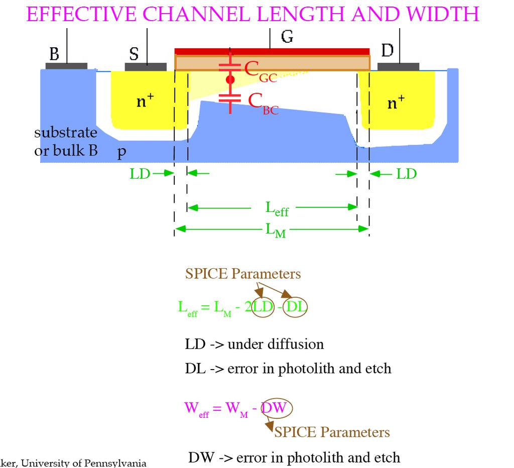
26 + n LD n+ LD + n n+ 26
27 (nmos, pmos) Model Depletion Region Capacitances 27
 = CoxWLD CGD0(overlap) =")

28 MOSFET CAPACITANCES Recall Cox = COX and tox = TOX in SPICE CGS0(overlap) = CoxWLD CGD0(overlap) = CoxWLD CGB0(overlap) = CoxWovLM SPICE: CoxLD = CGS0 = CGD0 in F/m; CoxWov = CGB0 in F/m Wov n+ LD W n+ Wov 28
")
29 CBG0 GatetoBulk Overlap Capacitance CBG0 Gate Extension Design Rule Weff SiO2 = Wov poly n+ p CGB0 = CoxWovLM C4 = 2λ = Wov = SiO2 Wov (conservative estimate) 29


30 Cgb, Cgs and Cgd n+ n+ Leff Leff n+ n+ MOSFET Saturation Region n+ n+ Leff 30
 = CoxWLeff + 2CGB0 + CGD0 + CGS0 Cutoff Region; Cg(tot) = CoxWLeff + 2CGB0 + CGD0 + CGS0 Linear Region; Cg(tot) = 2/3 CoxWLeff + 2CGB0 + CGD0 + CGS0 Saturation Region.")
31 GatetoBulk, Drain & Source Oxide Capacitances Summary + 2CGB CGB CGB0 Application of Oxide Capacitance Model:. Approximate: For hand calculations, assume that C gb, Cgd and Cgs are connected in parallel for each region of operation, i.e. Cg(tot) = CoxWLeff + 2CGB0 + CGD0 + CGS0 Cutoff Region; Cg(tot) = CoxWLeff + 2CGB0 + CGD0 + CGS0 Linear Region; Cg(tot) = 2/3 CoxWLeff + 2CGB0 + CGD0 + CGS0 Saturation Region. and use the maximum value Cg(tot) = CoxWLeff + 2CGB0 + CGD0 + CGS0 3

32 Depletion Region Capacitances > Cdb, Csb n+ n+ 32
 CJ =C j0 = = 0 xd 2 N A,N D 8 0 / ND m = MJ = grading coefficient m = ½ for abrupt junction [AS, AD > Source, Drain Areas in SPICE] [CJ > Cj0 in SPICE] [PB > O0 in SPICE] [MJ > m")
33 Depletion Region Capacitances > Cdb, Csb n+ + n V = Ext Bias > VSB, VDB + Qj = depletionregion charge A = junction area dq j A C j0 0 AS, AD CJ (F) C j 0V = = = m MJ dv V V 0, 0, PB 80 where 4 Si q 4 Si N A N D 2 (F/cm ) CJ =C j0 = = 0 xd 2 N A,N D 8 0 / ND m = MJ = grading coefficient m = ½ for abrupt junction [AS, AD > Source, Drain Areas in SPICE] [CJ > Cj0 in SPICE] [PB > O0 in SPICE] [MJ > m in SPICE] 33
34 Depletion Region Capacitances > Cdb, Csb Assume Weff = W 34
35 SUMMARY n+, p Junctions C j 0V = where / A C j0 0 AS, AD CJ (F) = m MJ V V 0, 0, PB 80 q 4 Si N A N D CJ =C j0 = 0 2 N A,N D 80 SPICE Parameters (F/cm2) Cj(0) = A Cj0 when V = 0 [AS, AD > Source, Drain Areas in SPICE] [CJ > Cj0 in SPICE] [PB > O0 in SPICE] [MJ > m in SPICE] 35
36 n+, p Junctions C j 0V = A C j0 0 AS, AD CJ = m MJ V V 0, 0, PB 80 voltage dependent EQUIVALENT LINEAR LARGE SIGNAL CAPACITANCE V 2Q Q j 0V 2 Q j 0V C eq = = = C 0V dv V 2 V V 2 V V j 2V 2 A C j0 80 V 2 m V m C j 0V C eq= [0, 0, ] V 2 V m NOTE voltage independent approximation 0 < Keq < > Voltage Equivalence Factor where V V V2 V = Ext Bias > VSB, VDB for nmos VBS, VBD for pmos C j 0V = A C j0 K eq =0 AS, AD CJ K eq 36
37 [PS, PD > Source, Drain Perimeters in SPICE] (F/cm2) [CJSW > C in SPICE] jsw [PBSW > O0SW in SPICE] [MJSW > m(sw) in SPICE] (F/cm) dq jsw C jsw 0V = = dv [XJ > xj in SPICE] P C jsw 0 PS, PD CJSW = m0sw MJSW V V 0, 0, PBSW 80sw m0 sw (F) m0 sw V2 V Recall for n+, p8junctions 0sw K eq 0 sw= [0, 0, 0V 2 V 0 m0 sw dq j A C j0 80 0sw AS, AD CJ 80sw C j 0V = = = (F) m MJ V junction V m(sw) = ½ dv for an abrupt 0, 0, PB 80 ] 37
38 dq jsw C jsw 0V = = dv P C jsw 0 PS, PD CJSW = MJSW V m0sw V 0, 0, PBSW 80sw voltage dependent voltage independent approximation where V V V2 V = Ext Bias > VSB, VDB for nmos VBS, VBD for pmos 38

39 4 CJ =.35 x 08 F/cm2 CJSW = 5.83 x 02 F/cm PB = V PBSW = V XJ = x 04 cm MJ = MJSW = ½ D n+ n+ S 39
40 C j 0V = A C j0 K eq = AD CJ K eq MJ V2 PB K eq = [0, 0V 2 V 0 MJ PB MJ V 0, PB ] CJ =.35 x 08 F/cm2 CJSW = 5.83 x 02 F/cm PB = V PBSW = V XJ = x 04 cm MJ = MJSW = /2 / V 5V 0.5 V /2 = [0, 0, ]= V 0.5 V V v C jsw 0V =P C jsw K eq 0sw =PD CJSW K eq 0sw MJSW V2 PBSW K eq 0 sw= [0, 0V 2 V 0 MJSW PBSW /2 MJSW V 0, PBSW ] / 2 = V [0, 5 V 0, 0.5 V ]=0.53 K eq 05V 0.5 V 0.975V v 40


41 CJ =.35 x 08 F/cm2 CJSW = 5.83 x 02 F/cm PB = V PBSW = V XJ = x 04 cm MJ = MJSW = / C j 0V = A C j0 K eq = AD CJ K eq =055 x 0 cm 0.35 x 0 F / cm 0.52=3.86 ff C jsw 0V =P C jsw K eq 0 sw =PD CJSW K eq 0 sw = 02.5 x 0 3 cm x 0 2 F / cm 0.53=7.72 ff C db = AD CJ K eq,pd CJSW K eq 0sw =.58 ff 4
42 MOSFET CAPACITANCE SUMMARY OXIDE CAPACITANCES Cgb = COX WLeff + CGB0 Cgd = (/2) COX WLeff + CGD0 Cgs = (2/3) COX WLeff + CGS0 Leff = LM 2LD DEPLETION CAPACITANCES Csb = Cj(VSB) + Cjsw(VSB) Cdb = Cj(VDB) + Cjsw(VDB) C j 0V = 0 AS, AD CJ 0 AS, AD CJ K eq Assume: AS = AD MJ V 0, MJ MJ V V PB PB K eq = [0, 2 0, ] 0V 2 V 0 MJ PB PB C jsw 0V = 0 PS, PD CJSW 0 PS, PD CJSW K eq 0 sw Assume: PS = PD MJSW V 0, PBSW V 2 MJSW V MJSW PBSW K eq 0 sw= [0, 0, ] 0V 2 V 0 MJSW PBSW PBSW 42
43 Short Channel Effects Leff xj Velocity saturation limit Reduced electron, hole mobility Reduced threshold voltage V T0 Narrow Channel Effects W xdm Increased threshold voltage V T0 Subthreshold Current VGS < VT0 Nonzero drain current when V < VT0 GS 43
")
44 SHORT CHANNEL ISSUES v sat cm V cm2 70 =0 /0 = sec cm V sec I D 0sat =W v sat C ox 0V GS V T 7n0 7n 0eff,50V GS V T (Lvl 3) 44
45 SHORT CHANNEL ISSUES CONT. Short Channel Effect Leff xj (source, drain diffusion depth) G S n+ pn+ depletion region G D n+ QB0 Leff xj pn+ depletion region VGS induced depletion region Q ox Q B0 V T0 0long channel =V FB 28 F C ox C ox S D n+ n+ Leff QB0(sc) QB0(sc) << QB0 VT0 (short channel) = VT0 (long channel) ΔVT


46 NARROW CHANNEL ISSUES Narrow Channel Effect W xdm (depletion region depth) fieldoxide W gateoxide Gate Extension design rule fieldoxide QB0(nc) QB0(nc) > QB0 Q ox Q B0 V T0 0long channel =V FB 28 F C ox C ox 46
47 I D 0 subthreshold =I S e V GS n kt / q V DS 0 e kt /q 0,6V DS + 4Si t ox subthreshold swing coefficient: n, 4ox t Si 7 C ox W kt 2 I S 0 L q [SPICE Parameter: N0 > n subthreshold swing coefficient NOTE: ID (subthreshold) is leakage current for stronginversion operation ID (subthreshold) is primary current for weakinversion operation + J. Rabaey, A. Chandrakasan and B. Nikolic; Digital Integrated Circuits 2nd Edition, Prentice Hall, 2003, pp99. 47
48 (MOSIS: Level 3 model used for min feature size µm) (MOSIS: BISIM3 model used for min feature size < µm) 48
49 Complexity of SPICE Models vs. Time BSIM4v6.5 (2009) EKV = EnzKrummenacherVittoz (EKV) model is for lowpower analog circuit simulation. SPICE Parameter Calculator Rochester Institute of Technology 49
50 MOS SPICE MODEL PARAMETERS Name Model Parameters LEVEL Model type (, 2, or 3) L W LD WD Channel Channel Lateral Lateral VTO U0 KP GAMMA PHI LAMBDA Zerobias threshold voltage Mobility Transconductance Bulk threshold parameter Surface potential Channellength modulation (LEVEL = and 2) RD RS RG RB RDS RSH NRS IS JS PB length (designer input) width (designer input) diffusion length diffusion width Drain ohmic resistance Source ohmic resistance Gate ohmic resistance Bulk ohmic resistance Drainsource shunt resistance Drainsource diffusion sheet Resistance Number of squares of RD, RS Bulk pn saturation current Bulk pn saturation/current area Bulk pn potential Units m m m m V cm**2/vs A/V**2 V**/2 V /V Ohms Ohms Ohms Ohms Ohms Ohms/sq. A A/m**2 V 50
51 MOS SPICE MODEL PARAMETERS CONT. Name Model Parameters Units LEVEL Model type (, 2, or 3) CBD CBS CJ CJSW MJ MJSW FC CGSO CGDO CGBO Bulkdrain zerobias pn cap (not used) F Bulksource zerobias pn cap (not used) F Bulk pn zerobias bottom cap/area F/m**2 Bulk pn zerobias perimeter cap/length F/m Bulk pn bottom grading coefficient Bulk pn sidewall grading coefficient Empirical bulk pn forwardbias cap coefficient Gatesource overlap cap/channel width F/m Gatedrain overlap cap/channel width F/m Gatebulk overlap cap/channel width F/m NSUB NSS NFS TOX TPG XJ Substate doping density Surfacestate density Fast surfacestate density Oxide thickness Gate material type: + = opposite of substrate, = same as substrate, 0 = aluminum Metallurgical junction depth /cm**3 /cm**2 /cm**2 m m 5
52 MOS SPICE MODEL PARAMETERS CONT. Name Model Parameters Units LEVEL Model type (, 2, or 3) UCRIT DELTA THETA ETA KAPPA Mobility degradation critical field V/cm (LEVEL=2) Empirical mobility degradation exponent (LEVEL=2) Maximum carrier drift velocity (Level=2) m/s Empirical channel charge coefficient (LEVEL=2) Empirical Fraction of channel charge attributed to drain (Level=2) Empirical channel width effect on VT Empirical mobility modulation (LEVEL=3) /V Empirical static feedback on VT (LEVEL=3) Empirical saturation field factor (LEVEL=3) KF AF Flicker noise coefficient Flicker noise exponent UEXP VMAX NEFF XQC 52
53 Level 3 SPICE Parameters KP (in A/V2) = k'n (k'p) VT0 (in volts) = VTn (VTp) U0 (in cm2/{vs}) = µn (µp) 53
ESE 570: Digital Integrated Circuits and VLSI Fundamentals
 ESE 570: Digital Integrated Circuits and VLSI Fundamentals Lec 6: January 30, 2018 MOS Operating Regions, pt. 2 Lecture Outline! Operating Regions (review) " Subthreshold " Resistive " Saturation! Intro.
The Devices. Devices
 The The MOS Transistor Gate Oxyde Gate Source n+ Polysilicon Drain n+ Field-Oxyde (SiO 2 ) p-substrate p+ stopper Bulk Contact CROSS-SECTION of NMOS Transistor Cross-Section of CMOS Technology MOS transistors
! MOS Capacitances. " Extrinsic. " Intrinsic. ! Lumped Capacitance Model. ! First Order Capacitor Summary. ! Capacitance Implications
 ESE 570: Digital Integrated Circuits and VLSI Fundamentals Lec 7: February, 07 MOS SPICE Models, MOS Parasitic Details Lecture Outline! MOS Capacitances " Extrinsic " Intrinsic! Lumped Capacitance Model!
ESE 570: Digital Integrated Circuits and VLSI Fundamentals
 ESE 570: Digital Integrated Circuits and VLSI Fundamentals Lec 7: February 4, 2016 MOS SPICE Models, MOS Parasitic Details Lecture Outline! MOS Capacitances " Extrinsic " Intrinsic! Lumped Capacitance
University of Pennsylvania Department of Electrical Engineering. ESE 570 Midterm Exam March 14, 2013 FORMULAS AND DATA
 University of Pennsylvania Department of Electrical Engineering ESE 570 Midterm Exam March 4, 03 FORMULAS AND DATA. PHYSICAL CONSTANTS: n i = intrinsic concentration undoped) silicon =.45 x 0 0 cm -3 @
EE 560 MOS TRANSISTOR THEORY PART 2. Kenneth R. Laker, University of Pennsylvania
 1 EE 560 MOS TRANSISTOR THEORY PART nmos TRANSISTOR IN LINEAR REGION V S = 0 V G > V T0 channel SiO V D = small 4 C GC C BC substrate depletion region or bulk B p nmos TRANSISTOR AT EDGE OF SATURATION
Circuits. L2: MOS Models-2 (1 st Aug. 2013) B. Mazhari Dept. of EE, IIT Kanpur. B. Mazhari, IITK. G-Number
 B. Mazhari Dept. of EE, IIT Kanpur. B. Mazhari, IITK. G-Number") EE610: CMOS Analog Circuits L: MOS Models- (1 st Aug. 013) B. Mazhari Dept. of EE, IIT Kanpur 3 NMOS Models MOS MODEL Above Threshold Subthreshold ( GS > TN ) ( GS < TN ) Saturation ti Ti Triode ( DS >
EE610: CMOS Analog Circuits L: MOS Models- (1 st Aug. 013) B. Mazhari Dept. of EE, IIT Kanpur 3 NMOS Models MOS MODEL Above Threshold Subthreshold ( GS > TN ) ( GS < TN ) Saturation ti Ti Triode ( DS >
N Channel MOSFET level 3
 N Channel MOSFET level 3 mosn3 NSource NBulk NSource NBulk NSource NBulk NSource (a) (b) (c) (d) NBulk Figure 1: MOSFET Types Form: mosn3: instance name n 1 n n 3 n n 1 is the drain node, n is the gate
EEC 118 Lecture #2: MOSFET Structure and Basic Operation. Rajeevan Amirtharajah University of California, Davis Jeff Parkhurst Intel Corporation
 EEC 118 Lecture #2: MOSFET Structure and Basic Operation Rajeevan Amirtharajah University of California, Davis Jeff Parkhurst Intel Corporation Announcements Lab 1 this week, report due next week Bring
The Devices: MOS Transistors
 The Devices: MOS Transistors References: Semiconductor Device Fundamentals, R. F. Pierret, Addison-Wesley Digital Integrated Circuits: A Design Perspective, J. Rabaey et.al. Prentice Hall NMOS Transistor
The Devices. Digital Integrated Circuits A Design Perspective. Jan M. Rabaey Anantha Chandrakasan Borivoje Nikolic. July 30, 2002
 Digital Integrated Circuits A Design Perspective Jan M. Rabaey Anantha Chandrakasan Borivoje Nikolic The Devices July 30, 2002 Goal of this chapter Present intuitive understanding of device operation Introduction
ELEC 3908, Physical Electronics, Lecture 26. MOSFET Small Signal Modelling
 ELEC 3908, Physical Electronics, Lecture 26 MOSFET Small Signal Modelling Lecture Outline MOSFET small signal behavior will be considered in the same way as for the diode and BJT Capacitances will be considered
ECE 342 Electronic Circuits. 3. MOS Transistors
 ECE 342 Electronic Circuits 3. MOS Transistors Jose E. Schutt-Aine Electrical & Computer Engineering University of Illinois jschutt@emlab.uiuc.edu 1 NMOS Transistor Typically L = 0.1 to 3 m, W = 0.2 to
APPENDIX A: Parameter List
 APPENDIX A: Parameter List A.1 BSIM3v3 Model Control Parameters none level BSIMv3 model selector 8 none Mobmod mobmod Mobility model selector 1 none Capmod capmod Flag for the short channel 1 none capacitance
MOSFET: Introduction
 E&CE 437 Integrated VLSI Systems MOS Transistor 1 of 30 MOSFET: Introduction Metal oxide semiconductor field effect transistor (MOSFET) or MOS is widely used for implementing digital designs Its major
EEC 116 Lecture #3: CMOS Inverters MOS Scaling. Rajeevan Amirtharajah University of California, Davis Jeff Parkhurst Intel Corporation
 EEC 116 Lecture #3: CMOS Inverters MOS Scaling Rajeevan Amirtharajah University of California, Davis Jeff Parhurst Intel Corporation Outline Review: Inverter Transfer Characteristics Lecture 3: Noise Margins,
Practice 3: Semiconductors
 Practice 3: Semiconductors Digital Electronic Circuits Semester A 2012 VLSI Fabrication Process VLSI Very Large Scale Integration The ability to fabricate many devices on a single substrate within a given
Lecture 3: CMOS Transistor Theory
 Lecture 3: CMOS Transistor Theory Outline Introduction MOS Capacitor nmos I-V Characteristics pmos I-V Characteristics Gate and Diffusion Capacitance 2 Introduction So far, we have treated transistors
VLSI Design The MOS Transistor
 VLSI Design The MOS Transistor Frank Sill Torres Universidade Federal de Minas Gerais (UFMG), Brazil VLSI Design: CMOS Technology 1 Outline Introduction MOS Capacitor nmos I-V Characteristics pmos I-V
EE 560 MOS TRANSISTOR THEORY
 1 EE 560 MOS TRANSISTOR THEORY PART 1 TWO TERMINAL MOS STRUCTURE V G (GATE VOLTAGE) 2 GATE OXIDE SiO 2 SUBSTRATE p-type doped Si (N A = 10 15 to 10 16 cm -3 ) t ox V B (SUBSTRATE VOLTAGE) EQUILIBRIUM:
MOS Transistor I-V Characteristics and Parasitics
 ECEN454 Digital Integrated Circuit Design MOS Transistor I-V Characteristics and Parasitics ECEN 454 Facts about Transistors So far, we have treated transistors as ideal switches An ON transistor passes
EKV MOS Transistor Modelling & RF Application
 HP-RF MOS Modelling Workshop, Munich, February 15-16, 1999 EKV MOS Transistor Modelling & RF Application Matthias Bucher, Wladek Grabinski Electronics Laboratory (LEG) Swiss Federal Institute of Technology,
APPENDIX A: Parameter List
 APPENDIX A: Parameter List A.1 BSIM3v3 Model Control Parameters none level BSIMv3 model selector 8 none Mobmod mobmod Mobility model selector 1 none Capmod capmod Flag for the short channel 2 none capacitance
EE5311- Digital IC Design
 EE5311- Digital IC Design Module 1 - The Transistor Janakiraman V Assistant Professor Department of Electrical Engineering Indian Institute of Technology Madras Chennai October 28, 2017 Janakiraman, IITM
MOS Transistors. Prof. Krishna Saraswat. Department of Electrical Engineering Stanford University Stanford, CA
 MOS Transistors Prof. Krishna Saraswat Department of Electrical Engineering S Stanford, CA 94305 saraswat@stanford.edu 1 1930: Patent on the Field-Effect Transistor! Julius Lilienfeld filed a patent describing
Conduction in Semiconductors -Review
 Conduction in Semiconductors Review Intrinsic (undoped) Semiconductors intrinsic carrier concentration n i =.45x0 0 cm 3, at room temp. n = p = n i, in intrinsic (undoped) material n number of electrons,
CMPEN 411 VLSI Digital Circuits. Lecture 03: MOS Transistor
 CMPEN 411 VLSI Digital Circuits Lecture 03: MOS Transistor Kyusun Choi [Adapted from Rabaey s Digital Integrated Circuits, Second Edition, 2003 J. Rabaey, A. Chandrakasan, B. Nikolic] CMPEN 411 L03 S.1
Integrated Circuits & Systems
 Federal University of Santa Catarina Center for Technology Computer Science & Electronics Engineering Integrated Circuits & Systems INE 5442 Lecture 10 MOSFET part 1 guntzel@inf.ufsc.br ual-well Trench-Isolated
ESE 570: Digital Integrated Circuits and VLSI Fundamentals
 ESE 570: Digital Integrated Circuits and VLSI Fundamentals Lec 5: January 25, 2018 MOS Operating Regions, pt. 1 Lecture Outline! 3 Regions of operation for MOSFET " Subthreshold " Linear " Saturation!
FIELD-EFFECT TRANSISTORS
 FIEL-EFFECT TRANSISTORS 1 Semiconductor review 2 The MOS capacitor 2 The enhancement-type N-MOS transistor 3 I-V characteristics of enhancement MOSFETS 4 The output characteristic of the MOSFET in saturation
MOS Transistor Theory
 CHAPTER 3 MOS Transistor Theory Outline 2 1. Introduction 2. Ideal I-V Characteristics 3. Nonideal I-V Effects 4. C-V Characteristics 5. DC Transfer Characteristics 6. Switch-level RC Delay Models MOS
Digital Integrated Circuits A Design Perspective. Jan M. Rabaey Anantha Chandrakasan Borivoje Nikolic. The Devices. July 30, Devices.
 Digital Integrated Circuits A Design Perspective Jan M. Rabaey Anantha Chandrakasan Borivoje Nikolic The July 30, 2002 1 Goal of this chapter Present intuitive understanding of device operation Introduction
Fundamentals of the Metal Oxide Semiconductor Field-Effect Transistor
 Triode Working FET Fundamentals of the Metal Oxide Semiconductor Field-Effect Transistor The characteristics of energy bands as a function of applied voltage. Surface inversion. The expression for the
APPENDIX D: Binning BSIM3v3 Parameters
 APPENDIX D: Binning BSIM3v3 Parameters Below is a list of all BSIM3v3 model parameters which can or cannot be binned. All model parameters which can be binned follow the following implementation: P L P
EE115C Winter 2017 Digital Electronic Circuits. Lecture 3: MOS RC Model, CMOS Manufacturing
 EE115C Winter 2017 Digital Electronic Circuits Lecture 3: MOS RC Model, CMOS Manufacturing Agenda MOS Transistor: RC Model (pp. 104-113) S R on D CMOS Manufacturing Process (pp. 36-46) S S C GS G G C GD
The Physical Structure (NMOS)
") The Physical Structure (NMOS) Al SiO2 Field Oxide Gate oxide S n+ Polysilicon Gate Al SiO2 SiO2 D n+ L channel P Substrate Field Oxide contact Metal (S) n+ (G) L W n+ (D) Poly 1 Transistor Resistance Two
The Physical Structure (NMOS) Al SiO2 Field Oxide Gate oxide S n+ Polysilicon Gate Al SiO2 SiO2 D n+ L channel P Substrate Field Oxide contact Metal (S) n+ (G) L W n+ (D) Poly 1 Transistor Resistance Two
Lecture 4: CMOS Transistor Theory
 Introduction to CMOS VLSI Design Lecture 4: CMOS Transistor Theory David Harris, Harvey Mudd College Kartik Mohanram and Steven Levitan University of Pittsburgh Outline q Introduction q MOS Capacitor q
Device Models (PN Diode, MOSFET )
") Device Models (PN Diode, MOSFET ) Instructor: Steven P. Levitan steve@ece.pitt.edu TA: Gayatri Mehta, José Martínez Book: Digital Integrated Circuits: A Design Perspective; Jan Rabaey Lab Notes: Handed
Device Models (PN Diode, MOSFET ) Instructor: Steven P. Levitan steve@ece.pitt.edu TA: Gayatri Mehta, José Martínez Book: Digital Integrated Circuits: A Design Perspective; Jan Rabaey Lab Notes: Handed
ESE 570 MOS TRANSISTOR THEORY Part 1. Kenneth R. Laker, University of Pennsylvania, updated 5Feb15
 ESE 570 MOS TRANSISTOR THEORY Part 1 TwoTerminal MOS Structure 2 GATE Si Oxide interface n n Mass Action Law VB 2 Chemical Periodic Table Donors American Chemical Society (ACS) Acceptors Metalloids 3 Ideal
EE105 Fall 2014 Microelectronic Devices and Circuits. NMOS Transistor Capacitances: Saturation Region
 EE105 Fall 014 Microelectronic Devices and Circuits Prof. Ming C. Wu wu@eecs.berkeley.edu 511 Sutardja Dai Hall (SDH) 1 NMOS Transistor Capacitances: Saturation Region Drain no longer connected to channel
EE105 - Fall 2006 Microelectronic Devices and Circuits
 EE105 - Fall 2006 Microelectronic Devices and Circuits Prof. Jan M. Rabaey (jan@eecs) Lecture 7: MOS Transistor Some Administrative Issues Lab 2 this week Hw 2 due on We Hw 3 will be posted same day MIDTERM
(S&S ) PMOS: holes flow from Source to Drain. from Source to Drain. W.-Y. Choi. Electronic Circuits 2 (09/1)
 PMOS: holes flow from Source to Drain. from Source to Drain. W.-Y. Choi. Electronic Circuits 2 (09/1)") (S&S 4.1 4.3) NMOS: electrons flow from Source to Drain PMOS: holes flow from Source to Drain In cut-off ( v < V ), i = 0 GS t D NMOS I-V Characteristics In triode, ( v > V but v v v ) GS t DS GS T W 1
(S&S 4.1 4.3) NMOS: electrons flow from Source to Drain PMOS: holes flow from Source to Drain In cut-off ( v < V ), i = 0 GS t D NMOS I-V Characteristics In triode, ( v > V but v v v ) GS t DS GS T W 1
Today s lecture. EE141- Spring 2003 Lecture 4. Design Rules CMOS Inverter MOS Transistor Model
 - Spring 003 Lecture 4 Design Rules CMOS Inverter MOS Transistor Model Today s lecture Design Rules The CMOS inverter at a glance An MOS transistor model for manual analysis Important! Labs start next
Chapter 4 Field-Effect Transistors
 Chapter 4 Field-Effect Transistors Microelectronic Circuit Design Richard C. Jaeger Travis N. Blalock 5/5/11 Chap 4-1 Chapter Goals Describe operation of MOSFETs. Define FET characteristics in operation
ECE 497 JS Lecture - 12 Device Technologies
 ECE 497 JS Lecture - 12 Device Technologies Spring 2004 Jose E. Schutt-Aine Electrical & Computer Engineering University of Illinois jose@emlab.uiuc.edu 1 NMOS Transistor 2 ρ Source channel charge density
The Devices. Digital Integrated Circuits A Design Perspective. Jan M. Rabaey Anantha Chandrakasan Borivoje Nikolic. July 30, 2002
 igital Integrated Circuits A esign Perspective Jan M. Rabaey Anantha Chandrakasan Borivoje Nikolic The evices July 30, 2002 Goal of this chapter Present intuitive understanding of device operation Introduction
Device Models (PN Diode, MOSFET )
") Device Models (PN Diode, MOSFET ) Instructor: Steven P. Levitan steve@ece.pitt.edu TA: Gayatri Mehta, José Martínez Book: Digital Integrated Circuits: A Design Perspective; Jan Rabaey Lab Notes: Handed
Device Models (PN Diode, MOSFET ) Instructor: Steven P. Levitan steve@ece.pitt.edu TA: Gayatri Mehta, José Martínez Book: Digital Integrated Circuits: A Design Perspective; Jan Rabaey Lab Notes: Handed
Lecture 5: CMOS Transistor Theory
 Lecture 5: CMOS Transistor Theory Slides courtesy of Deming Chen Slides based on the initial set from David Harris CMOS VLSI Design Outline q q q q q q q Introduction MOS Capacitor nmos I-V Characteristics
ECE 546 Lecture 10 MOS Transistors
 ECE 546 Lecture 10 MOS Transistors Spring 2018 Jose E. Schutt-Aine Electrical & Computer Engineering University of Illinois jesa@illinois.edu NMOS Transistor NMOS Transistor N-Channel MOSFET Built on p-type
The Devices. Jan M. Rabaey
 The Devices Jan M. Rabaey Goal of this chapter Present intuitive understanding of device operation Introduction of basic device equations Introduction of models for manual analysis Introduction of models
ELEC 3908, Physical Electronics, Lecture 23. The MOSFET Square Law Model
 ELEC 3908, Physical Electronics, Lecture 23 The MOSFET Square Law Model Lecture Outline As with the diode and bipolar, have looked at basic structure of the MOSFET and now turn to derivation of a current
CHAPTER 5 MOS FIELD-EFFECT TRANSISTORS
 CHAPTER 5 MOS FIELD-EFFECT TRANSISTORS 5.1 The MOS capacitor 5.2 The enhancement-type N-MOS transistor 5.3 I-V characteristics of enhancement mode MOSFETS 5.4 The PMOS transistor and CMOS technology 5.5
Lecture 10 MOSFET (III) MOSFET Equivalent Circuit Models
 MOSFET Equivalent Circuit Models") Lecture 1 MOSFET (III) MOSFET Equivalent Circuit Models Outline Lowfrequency smallsignal equivalent circuit model Highfrequency smallsignal equivalent circuit model Reading Assignment: Howe and Sodini;
Lecture 1 MOSFET (III) MOSFET Equivalent Circuit Models Outline Lowfrequency smallsignal equivalent circuit model Highfrequency smallsignal equivalent circuit model Reading Assignment: Howe and Sodini;
CHAPTER 3 - CMOS MODELS
 CMOS Analog Circuit Design Page 3.-1 CHAPTER 3 - CMOS MODELS Chapter Outline 3.1 MOS Structure and Operation 3.2 Large signal MOS models suitable for hand calculations 3.3 Extensions of the large signal
Virtual Device Simulation. Virtual Process Integration
 : CMOS Process and Device Simulation Virtual Device Simulation Virtual Process Integration Dr Zhou Xing Office: S1-B1c-95 Phone: 6790-4532 Email: exzhou@ntu.edu.sg Web: http://www.ntu.edu.sg/home/exzhou/teaching//
II III IV V VI B C N. Al Si P S. Zn Ga Ge As Se Cd In Sn Sb Te. Silicon (Si) the dominating material in IC manufacturing
 the dominating material in IC manufacturing") II III IV V VI B N Al Si P S Zn Ga Ge As Se d In Sn Sb Te Silicon (Si) the dominating material in I manufacturing ompound semiconductors III - V group: GaAs GaN GaSb GaP InAs InP InSb... The Energy Band
II III IV V VI B N Al Si P S Zn Ga Ge As Se d In Sn Sb Te Silicon (Si) the dominating material in I manufacturing ompound semiconductors III - V group: GaAs GaN GaSb GaP InAs InP InSb... The Energy Band
EE105 - Fall 2005 Microelectronic Devices and Circuits
 EE105 - Fall 005 Microelectronic Devices and Circuits ecture 7 MOS Transistor Announcements Homework 3, due today Homework 4 due next week ab this week Reading: Chapter 4 1 ecture Material ast lecture
Lecture 10 MOSFET (III) MOSFET Equivalent Circuit Models
 MOSFET Equivalent Circuit Models") Lecture 10 MOSFET (III) MOSFET Equivalent Circuit Models Outline Lowfrequency smallsignal equivalent circuit model Highfrequency smallsignal equivalent circuit model Reading Assignment: Howe and Sodini;
Lecture 10 MOSFET (III) MOSFET Equivalent Circuit Models Outline Lowfrequency smallsignal equivalent circuit model Highfrequency smallsignal equivalent circuit model Reading Assignment: Howe and Sodini;
MOS Transistor Theory
 MOS Transistor Theory So far, we have viewed a MOS transistor as an ideal switch (digital operation) Reality: less than ideal EE 261 Krish Chakrabarty 1 Introduction So far, we have treated transistors
MOSFET Capacitance Model
 MOSFET Capacitance Model So far we discussed the MOSFET DC models. In real circuit operation, the device operates under time varying terminal voltages and the device operation can be described by: 1 small
Lecture Outline. ESE 570: Digital Integrated Circuits and VLSI Fundamentals. Review: MOS Capacitor with External Bias
 ESE 57: Digital Integrated Circuits and VLSI Fundamentals Lec 5: Januar 6, 17 MOS Operating Regions, pt. 1 Lecture Outline! 3 Regions of operation for MOSFET " Subthreshold " Linear " Saturation! Level
LECTURE 3 MOSFETS II. MOS SCALING What is Scaling?
 LECTURE 3 MOSFETS II Lecture 3 Goals* * Understand constant field and constant voltage scaling and their effects. Understand small geometry effects for MOS transistors and their implications modeling and
MOS Transistor Theory MOSFET Symbols Current Characteristics of MOSFET. MOS Symbols and Characteristics. nmos Enhancement Transistor
 MOS Transistor Theory MOSFET Symbols Current Characteristics of MOSFET Calculation of t and Important 2 nd Order Effects SmallSignal Signal MOSFET Model Summary Material from: CMOS LSI Design By Weste
Nanoscale CMOS Design Issues
 Nanoscale CMOS Design Issues Jaydeep P. Kulkarni Assistant Professor, ECE Department The University of Texas at Austin jaydeep@austin.utexas.edu Fall, 2017, VLSI-1 Class Transistor I-V Review Agenda Non-ideal
Chapter 2 CMOS Transistor Theory. Jin-Fu Li Department of Electrical Engineering National Central University Jungli, Taiwan
 Chapter 2 CMOS Transistor Theory Jin-Fu Li Department of Electrical Engineering National Central University Jungli, Taiwan Outline Introduction MOS Device Design Equation Pass Transistor Jin-Fu Li, EE,
The simulated two volt performance of CMOS circuits with submicron transistors
 Lehigh University Lehigh Preserve Theses and Dissertations 1992 The simulated two volt performance of CMOS circuits with submicron transistors Christopher John Younger Lehigh University Follow this and
MOS Device Modeling. C.K. Ken Yang UCLA Courtesy of Agilent eesoft EE 215B
 MOS Device Modeling C.K. Ken Yang UCLA yangck@ucla.edu Courtesy of Agilent eesoft 1 Overview Reading Rabaey 3.3 W&H 2.2-2.4 Overview This class will look at the iv and CV characteristics of an MOS device
Lecture 15: MOS Transistor models: Body effects, SPICE models. Context. In the last lecture, we discussed the modes of operation of a MOS FET:
 Lecture 15: MOS Transistor models: Body effects, SPICE models Context In the last lecture, we discussed the modes of operation of a MOS FET: oltage controlled resistor model I- curve (Square-Law Model)
APPENDIX D: Model Parameter Binning
 APPENDIX D: Model Parameter Binning Below is the information on parameter binning regarding which model parameters can or cannot be binned. All those parameters which can be binned follow this implementation:
Content. MIS Capacitor. Accumulation Depletion Inversion MOS CAPACITOR. A Cantoni Digital Switching
 Content MIS Capacitor Accumulation Depletion Inversion MOS CAPACITOR 1 MIS Capacitor Metal Oxide C ox p-si C s Components of a capacitance model for the MIS structure 2 MIS Capacitor- Accumulation ρ( x)
Introduction and Background
 Analog CMOS Integrated Circuit Design Introduction and Background Dr. Jawdat Abu-Taha Department of Electrical and Computer Engineering Islamic University of Gaza jtaha@iugaza.edu.ps 1 Marking Assignments
MOS Transistor Properties Review
 MOS Transistor Properties Review 1 VLSI Chip Manufacturing Process Photolithography: transfer of mask patterns to the chip Diffusion or ion implantation: selective doping of Si substrate Oxidation: SiO
The Intrinsic Silicon
 The Intrinsic ilicon Thermally generated electrons and holes Carrier concentration p i =n i ni=1.45x10 10 cm-3 @ room temp Generally: n i = 3.1X10 16 T 3/2 e -1.21/2KT cm -3 T= temperature in K o (egrees
and V DS V GS V T (the saturation region) I DS = k 2 (V GS V T )2 (1+ V DS )
 I DS = k 2 (V GS V T )2 (1+ V DS )") ECE 4420 Spring 2005 Page 1 FINAL EXAMINATION NAME SCORE /100 Problem 1O 2 3 4 5 6 7 Sum Points INSTRUCTIONS: This exam is closed book. You are permitted four sheets of notes (three of which are your sheets
ECE 4420 Spring 2005 Page 1 FINAL EXAMINATION NAME SCORE /100 Problem 1O 2 3 4 5 6 7 Sum Points INSTRUCTIONS: This exam is closed book. You are permitted four sheets of notes (three of which are your sheets
ESE 570: Digital Integrated Circuits and VLSI Fundamentals
 ESE 570: Digital Integrated Circuits and VLSI Fundamentals Lec 4: January 23, 2018 MOS Transistor Theory, MOS Model Penn ESE 570 Spring 2018 Khanna Lecture Outline! CMOS Process Enhancements! Semiconductor
Practice 7: CMOS Capacitance
 Practice 7: CMOS Capacitance Digital Electronic Circuits Semester A 2012 MOSFET Capacitances MOSFET Capacitance Components 3 Gate to Channel Capacitance In general, the gate capacitance is similar to a
Lecture 11: MOS Transistor
 Lecture 11: MOS Transistor Prof. Niknejad Lecture Outline Review: MOS Capacitors Regions MOS Capacitors (3.8 3.9) CV Curve Threshold Voltage MOS Transistors (4.1 4.3): Overview Cross-section and layout
ECE-305: Fall 2017 MOS Capacitors and Transistors
 ECE-305: Fall 2017 MOS Capacitors and Transistors Pierret, Semiconductor Device Fundamentals (SDF) Chapters 15+16 (pp. 525-530, 563-599) Professor Peter Bermel Electrical and Computer Engineering Purdue
CMOS Digital Integrated Circuits Analysis and Design
 MOS igital ntegrated ircuits Analysis and esign hapter 4 Modeling of MOS ransistors Using SPE 1 ntroduction he SPE software that was distributed by U Berkeley beginning in the late 1970s had three built-in
! CMOS Process Enhancements. ! Semiconductor Physics. " Band gaps. " Field Effects. ! MOS Physics. " Cut-off. " Depletion.
 ESE 570: Digital Integrated Circuits and VLSI Fundamentals Lec 4: January 3, 018 MOS Transistor Theory, MOS Model Lecture Outline! CMOS Process Enhancements! Semiconductor Physics " Band gaps " Field Effects!
Lecture 04 Review of MOSFET
 ECE 541/ME 541 Microelectronic Fabrication Techniques Lecture 04 Review of MOSFET Zheng Yang (ERF 3017, email: yangzhen@uic.edu) What is a Transistor? A Switch! An MOS Transistor V GS V T V GS S Ron D
EECS130 Integrated Circuit Devices
 EECS130 Integrated Circuit Devices Professor Ali Javey 10/30/2007 MOSFETs Lecture 4 Reading: Chapter 17, 19 Announcements The next HW set is due on Thursday. Midterm 2 is next week!!!! Threshold and Subthreshold
Microelectronics Part 1: Main CMOS circuits design rules
 GBM8320 Dispositifs Médicaux telligents Microelectronics Part 1: Main CMOS circuits design rules Mohamad Sawan et al. Laboratoire de neurotechnologies Polystim! http://www.cours.polymtl.ca/gbm8320/! med-amine.miled@polymtl.ca!
Introduction to CMOS VLSI. Chapter 2: CMOS Transistor Theory. Harris, 2004 Updated by Li Chen, Outline
 Introduction to MOS VLSI Design hapter : MOS Transistor Theory copyright@david Harris, 004 Updated by Li hen, 010 Outline Introduction MOS apacitor nmos IV haracteristics pmos IV haracteristics Gate and
ECE 438: Digital Integrated Circuits Assignment #4 Solution The Inverter
 ECE 438: Digital Integrated Circuits Assignment #4 The Inverter Text: Chapter 5, Digital Integrated Circuits 2 nd Ed, Rabaey 1) Consider the CMOS inverter circuit in Figure P1 with the following parameters.
Final Examination EE 130 December 16, 1997 Time allotted: 180 minutes
 Final Examination EE 130 December 16, 1997 Time allotted: 180 minutes Problem 1: Semiconductor Fundamentals [30 points] A uniformly doped silicon sample of length 100µm and cross-sectional area 100µm 2
CMPEN 411 VLSI Digital Circuits. Lecture 04: CMOS Inverter (static view)
") CMPEN 411 VLSI Digital Circuits Lecture 04: CMOS Inverter (static view) Kyusun Choi [Adapted from Rabaey s Digital Integrated Circuits, Second Edition, 2003 J. Rabaey, A. Chandrakasan, B. Nikolic] CMPEN
CMPEN 411 VLSI Digital Circuits Lecture 04: CMOS Inverter (static view) Kyusun Choi [Adapted from Rabaey s Digital Integrated Circuits, Second Edition, 2003 J. Rabaey, A. Chandrakasan, B. Nikolic] CMPEN
Operation and Modeling of. The MOS Transistor. Second Edition. Yannis Tsividis Columbia University. New York Oxford OXFORD UNIVERSITY PRESS
 Operation and Modeling of The MOS Transistor Second Edition Yannis Tsividis Columbia University New York Oxford OXFORD UNIVERSITY PRESS CONTENTS Chapter 1 l.l 1.2 1.3 1.4 1.5 1.6 1.7 Chapter 2 2.1 2.2
Lecture 12: MOSFET Devices
 Lecture 12: MOSFET Devices Gu-Yeon Wei Division of Engineering and Applied Sciences Harvard University guyeon@eecs.harvard.edu Wei 1 Overview Reading S&S: Chapter 5.1~5.4 Supplemental Reading Background
VLSI Design and Simulation
 VLSI Design and Simulation Performance Characterization Topics Performance Characterization Resistance Estimation Capacitance Estimation Inductance Estimation Performance Characterization Inverter Voltage
Lecture Outline. ESE 570: Digital Integrated Circuits and VLSI Fundamentals. Review: MOSFET N-Type, P-Type. Semiconductor Physics.
 ESE 57: Digital Integrated Circuits and VLSI Fundamentals Lec 4: January 24, 217 MOS Transistor Theory, MOS Model Lecture Outline! Semiconductor Physics " Band gaps " Field Effects! MOS Physics " Cutoff
Chapter 2 MOS Transistor theory
 Chapter MOS Transistor theory.1 Introduction An MOS transistor is a majority-carrier device, which the current a conductg channel between the source and the dra is modulated by a voltage applied to the
SECTION: Circle one: Alam Lundstrom. ECE 305 Exam 5 SOLUTIONS: Spring 2016 April 18, 2016 M. A. Alam and M.S. Lundstrom Purdue University
 NAME: PUID: SECTION: Circle one: Alam Lundstrom ECE 305 Exam 5 SOLUTIONS: April 18, 2016 M A Alam and MS Lundstrom Purdue University This is a closed book exam You may use a calculator and the formula
ECE 342 Electronic Circuits. Lecture 6 MOS Transistors
 ECE 342 Electronic Circuits Lecture 6 MOS Transistors Jose E. Schutt-Aine Electrical & Computer Engineering University of Illinois jesa@illinois.edu 1 NMOS Transistor Typically L = 0.1 to 3 m, W = 0.2
P. R. Nelson 1 ECE418 - VLSI. Midterm Exam. Solutions
 P. R. Nelson 1 ECE418 - VLSI Midterm Exam Solutions 1. (8 points) Draw the cross-section view for A-A. The cross-section view is as shown below.. ( points) Can you tell which of the metal1 regions is the
CS/EE N-type Transistor
 CS/EE 6710 MOS Transistor Models Electrical Effects Propagation Delay N-type Transistor D + G Vds i electrons +Vgs S - 1 Another Cutaway View Thanks to National Central University for Some images Vgs Forms
ECEN474/704: (Analog) VLSI Circuit Design Spring 2018
 VLSI Circuit Design Spring 2018") ECEN474/704: (Analog) SI Circuit Design Spring 2018 ecture 2: MOS ransistor Modeling Sam Palermo Analog & Mixed-Signal Center exas A&M University Announcements If you haven t already, turn in your 0.18um
ECEN474/704: (Analog) SI Circuit Design Spring 2018 ecture 2: MOS ransistor Modeling Sam Palermo Analog & Mixed-Signal Center exas A&M University Announcements If you haven t already, turn in your 0.18um
1/13/12 V DS. I d V GS. C ox ( = f (V GS ,V DS ,V SB = I D. + i d + I ΔV + I ΔV BS V BS. 19 January 2012
 /3/ 9 January 0 Study the linear model of MOS transistor around an operating point." MOS in saturation: V GS >V th and V S >V GS -V th " VGS vi - I d = I i d VS I d = µ n ( L V V γ Φ V Φ GS th0 F SB F
ECE315 / ECE515 Lecture-2 Date:
 Lecture-2 Date: 04.08.2016 NMOS I/V Characteristics Discussion on I/V Characteristics MOSFET Second Order Effect NMOS I-V Characteristics ECE315 / ECE515 Gradual Channel Approximation: Cut-off Linear/Triode
! CMOS Process Enhancements. ! Semiconductor Physics. " Band gaps. " Field Effects. ! MOS Physics. " Cut-off. " Depletion.
 ESE 570: Digital Integrated Circuits and VLSI Fundamentals Lec 4: January 9, 019 MOS Transistor Theory, MOS Model Lecture Outline CMOS Process Enhancements Semiconductor Physics Band gaps Field Effects