Workshop WMB. Noise Modeling
|
|
|
- Gregory Dawson
- 5 years ago
- Views:
Transcription
1 Workshop WMB Noise Modeling Manfred Berroth, Markus Grözing, Stefan Heck, Alexander Bräckle University of Stuttgart, Germany WMB (IMS) Parameter Extraction Strategies For Compact Transistor Models IMS 9
2 Outline Motivation Fundamentals Noise Modeling Noise Measurements Parameter Extraction Application Low Noise Amplifier
3 Local network Access point Motivation Mobile phone Headset Mouse Printer Laptop Noise limits transmission distance!
4 PSD/KHz -8 Noise Fundamentals Antenna Noise Power Spectral Density db - max. Noise - Receiver Noise Cosmic Noise -4.. m λ
5 Fundamentals Noise is caused by spontaneous fluctuations. Spontaneous fluctuations limit the accuracy of measurements. The signal-to-noise ratio limits the range of any communications system. Three types of noise are present in electronic circuits: - Thermal noise - Shot noise - Flicker noise
6 Probability dp that the value of a fluctuating quantity is between x and x + dx Fundamentals Probability distribution ( ) dx Probability distribution function f(x): dp f x Average value of the n-th moment xn x n dp True fluctuating quantity: Most important average value real mean square: Example: Normal distribution p ( ξ) x f ( x) e σ σ π σ p ( ξ ) x x ξ u u σ ξ u u σ
7 Fundamentals Definition of Correlation x, y mean-free fluctuating quantities Uncorrelated: xy xy x if y x Correlation coefficient c x xy y c c uncorrelated completely correlated < c < partly correlated
8 Fundamentals Fourier Analysis Noise signal x(t) w(f) spectral intensity of the noise X w( f) df Amplifier example: Y ( t) h ( t) x ( t) ( time domain) y * ( f) g ( f) X ( f) ( frequency domain) y g ( f) w( f) df
9 Thermal Noise Available noise power in the frequency interval df at a resistance R at temperature T. P 4 with u R S p i 4 i ( f,t) R e kt p 4 kt ( f) p( f, T) R hf kt hf kt ( f,t) df (Planck's correction factor) at room temperature (3 K) termal noise is flat up to ~6 THz
10 Thermal Noise White Noise Sources S ir Diffusion Noise S ig 4 k T R 4 k Te G (all resistive parts of the circuit) (channel noise) f << τ Shot Noise S ij q I (e.g. pn-junctions) T absolute temperature T e electron gas temperature
11 Channel Noise Inversion Charge Model t ds id N L R 4kT (f) S + Wang et.al [7] + 3 D ox eff id ) ( ) ( L I W C 4kTµ (f) S inv eff ds Q µ R + Wang et.al [7] + DSeff DSeff T GS C eff ox 3 DSeff DSeff T GS DSeff T GS ) ( L E µ 4kTWC 3 ) ( ) (
12 BSiM Channel Noise S 4kT dseff 4 ktθtnoi (gm + I R + g DSeff id (f) + βtnoi(gm + gmbs) I D R ds d ds mbs ) θ TNOI R nb + T nb L gs E C L β TNOI R na + T na L gs E C L
13 Flicker Noise i f K f I f A E f f df Example MOSFET : S id K I f C f f d ( f) with A E f E A ' X L f f
14 Unified Model (Hung) Flicker- Noise S id (f) ktq µ α γ fc eff ' ox I d L d kti + L γ fwl N Aln N L A+ BN + N + N L + CN ( N ) L N + + B L ( ) ( N N + N N ) L C L
15 Amplifier Noise Power Spectral Density S i (f) -6 A /Hz I II f a I f µ f obs K K K M M f c Hz III M G f o f
16 Noisy Two-Port Noise Factor F S S i /N /N i Noise Figure NF log (F)
17 Noisy Two-Port P T n e i i i T T B G T k N B S T k S N S N S N F + k B G P T n e ( ) e T T k B G N +
18 Noisy Two-Port Interaction of Different Noise Sources e e e e e e a W W W W W e e e e e e a W W W W W e e e e e e a u u u u u u u + + +
19 Noisy Two-Port I U A I Noiseless Two-Port Z S U U S U I A Z U I A A U U + + A A I I + + I U A A F S N i i N S + U A + Z S I A / ( 8 kt f Re { Z }) S F 4R Z Γ n S opt Fmin + Z + Γ opt ZS
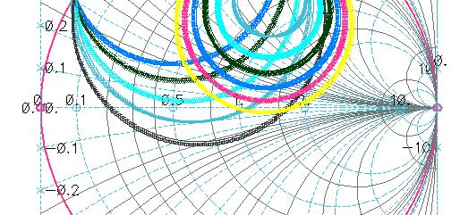
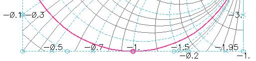
20 ector Network Analyzer Noise Test Setup Device Driver HP EE MATLAB Port Port Test Set IEEE 488. PC Noise Figure Metre Noise Source NPT 8 Tuner Γ NS Γ S Γ D Γ rcvr DUT NPT 8 Tuner Parameter Analyzer
21 Noise Hyperbolic of the used MOSFET 6 5 w µm l.35 µm 4 F 3 8 U ds, U GHz I d 9,7 ma F min.8 db
22 Minimum Noise Figure ersus Operating oltage 6 db F min U DS 3 5,8,4,6 4, U GS
23 Correlation Matrices ABCD Noiseless Two-Port C Trans A kt NF R n NF min R Y min R nyopt Rn Yopt n * opt Trans Trans C Z TAZC A T + AZ T: Transformation Matrix T + : Hermitian Conjugate Complex int Trans C C C Z,transistor Z,transistor Z,Rs Trans Trans C Y TZYC A T + ZY
24 Intrinsic Transistor Noise Model i > < i d > < g < i g > Admittance Noiseless < i d > Two-Port * < ig id > Series resistances already subtracted by correlation matrices * * Cross correlation between gate : and channel noise C < igig > < igid > B idig idi < > < d > Y * *
25 Device Parasitics Γ s, e Γ s, i Noise of Lossy Substrate
26 MOSFET Substrate Modeling Polysilicon Gate Drain Bulk Source Bulk R s R g R d n + n+ C sb R ch C db R dsb C sub R sb R db C sub
27 High Frequency Modeling of MOSFET Intrinsic Transistor Source and bulk connected!
28 High Frequency Model and Measurement real(ymodel(,)) real(ymeas(,)) real(ymodel(,)) real(ymeas(,)) freq, GHz freq, GHz real(ymodel(,)) real(ymeas(,)) real(ymodel(,)) real(ymeas(,)) freq, GHz freq, GHz
29 High Frequency Noise Model of MOSFETs Contact Pad Contact Pad All resistors generate thermal noise with the spectral density < i R > 4kT R
30 Induced Gate Noise Gate noise only induced by capacitive coupering < i > g 4 4kTggsB 3 < 6 i > ktr C 3 ω g gs gs an der Ziel, Noise in Solid-State Devices and Circuits, John Wiley & Sons, 986 Norton equivalent circuit
31 Deembedding with Correlation Matrices Y pad pad C kt Re( Y ) Y Z C Y y y -y y y -y Z z z z z -z -z Transformations Between Correlation Matrices C a -a a -a Equivalent Circuit of Pads Hillbrand und Russer, An efficient method for computer-aided analysis of linear amplifier networks, 976. C Trans A kt NF min R n R Y n opt NF min R R Y n Y opt n * opt ABCD Matrix
32 Parameter Extraction (MOSFET) After Deembedding of pad capacitances and inductances, the series resistances of gate and drain have to be deembedded: [ CZ,T ] [ TZ Y ] [ CA ] [ TA Z ] [ ] Rg C Z, T [ CZ,T ] kt Rd + + Hermitian Conjugation
33 Parameter Extraction (MOSFET) To deembed the substrate admittance, the correlation matrices have to be transformed to the admittance form: [ C ] [ T ] [ C ] [ T ] Y, T Z Y [ C ] [ C ] Y, T Y, T Z, T Z Y kt Re + Y sub
34 Parameter Extraction (MOSFET) To deembed the source resistance, the impedance form of the correlation matrix is required: [ C ] [ T ] [ C ] [ T ] Z, T Y Z Y, T [ ] [ ] int Rs C Z, T C Z, T kt Rs Y Z +
35 Measured Noise Parameters ( ds, gs, W394 µm)
36 Noise Figure of the MOSFET at a Source Impedance of 5 Ω db 8 F measurement simulation with parasitics simulation without parasitics GHz f
37 Noise Parameters ( DS, GS )
38 Minimum Noise Figure of the MOSFET F min, G ass db F min - measurement G ass - measurement F min - simulation GHz f
39 Sensitivity Analysis of all Noise Sources at 5 Ω F 5 9 db channel current noise MOSFET w µm lg.35 µm 3 R g thermal noise sources Rs R gs g ds GHz frequency U ds and U gs R d


40 Noise Circles Noise Matching L g improves the stability Gain Circles Z in gm jω L + + L + jω L jωc C s s g gs gs
41 Low Noise Amplifier

42 Layout 48 µm 69 µm 8 µm LNA 4GHz LNA 5GHz
43 Measurements of Low Noise Amplifier
44 Measurements of Low Noise Amplifier
45 Summary Analytical modeling of the noise spectral density High frequency noise model Noise parameter extraction Application of the model Low noise amplifier
46 References: [] A. van der Ziel, Noise, Prentice Hall, 954 [] H. Hillbrand, P. H. Russer, An Efficient Method for Computer Aided Noise Analysis of Linear Amplifier Networks, IEEE Trans. Circuits and Systems, ol. AS-3, no. 4, 976, pp [3] U. Basaran, Modellierung von Transistoren in CMOS/BiCMOS-Technologie zum Entwurf von rauscharmen erstärkern, Dissertation Universität Stuttgart, 7
47 Questions?
Transistor Noise Lecture 10 High Speed Devices
 Transistor Noise 1 Transistor Noise A very brief introduction to circuit and transistor noise. I an not an expert regarding noise Maas: Noise in Linear and Nonlinear Circuits Lee: The Design of CMOS RFIC
Lecture 14: Electrical Noise
 EECS 142 Lecture 14: Electrical Noise Prof. Ali M. Niknejad University of California, Berkeley Copyright c 2008 by Ali M. Niknejad A.M.Niknejad University of California, Berkeley EECS 142 Lecture 14 p.1/20
Two-Port Noise Analysis
 Berkeley Two-Port Noise Analysis Prof. Ali M. Niknejad U.C. Berkeley Copyright c 2015 by Ali M. Niknejad 1/26 Equivalent Noise Generators v 2 n Noisy Two-Port i 2 n Noiseless Two-Port Any noisy two port
6.776 High Speed Communication Circuits Lecture 10 Noise Modeling in Amplifiers
 6.776 High Speed Communication Circuits Lecture 10 Noise Modeling in Amplifiers Michael Perrott Massachusetts Institute of Technology March 8, 2005 Copyright 2005 by Michael H. Perrott Notation for Mean,
Analysis and Design of Analog Integrated Circuits Lecture 14. Noise Spectral Analysis for Circuit Elements
 Analysis and Design of Analog Integrated Circuits Lecture 14 Noise Spectral Analysis for Circuit Elements Michael H. Perrott March 18, 01 Copyright 01 by Michael H. Perrott All rights reserved. Recall
Transistor Noise Lecture 14, High Speed Devices
 Transistor Noise 016-03-03 Lecture 14, High Speed Devices 016 1 Transistor Noise A very brief introduction 016-03-0 Lecture 13, High Speed Devices 016 Summary hybrid p Noise is a randomly varying voltage/current
Device Models (PN Diode, MOSFET )
") Device Models (PN Diode, MOSFET ) Instructor: Steven P. Levitan steve@ece.pitt.edu TA: Gayatri Mehta, José Martínez Book: Digital Integrated Circuits: A Design Perspective; Jan Rabaey Lab Notes: Handed
Device Models (PN Diode, MOSFET ) Instructor: Steven P. Levitan steve@ece.pitt.edu TA: Gayatri Mehta, José Martínez Book: Digital Integrated Circuits: A Design Perspective; Jan Rabaey Lab Notes: Handed
Outline. Thermal noise, noise power and noise temperature. Noise in RLC single-ports. Noise in diodes and photodiodes
 3. Noise 1 Outline Thermal noise, noise power and noise temperature Noise in RLC single-ports Noise in diodes and photodiodes -port and multi-port noise parameters Noise temperature and noise parameter
EKV MOS Transistor Modelling & RF Application
 HP-RF MOS Modelling Workshop, Munich, February 15-16, 1999 EKV MOS Transistor Modelling & RF Application Matthias Bucher, Wladek Grabinski Electronics Laboratory (LEG) Swiss Federal Institute of Technology,
Self-heat Modeling of Multi-finger n-mosfets for RF-CMOS Applications
 Self-heat Modeling of Multi-finger n-mosfets for RF-CMOS Applications Hitoshi Aoki and Haruo Kobayashi Faculty of Science and Technology, Gunma University (RMO2D-3) Outline Research Background Purposes
Investigation of the Thermal Noise of MOS Transistors under Analog and RF Operating Conditions
 Investigation of the Thermal Noise of MOS Transistors under Analog and RF Operating Conditions Ralf Brederlow 1, Georg Wenig 2, and Roland Thewes 1 1 Infineon Technologies, Corporate Research, 2 Technical
CHAPTER 5 EFFECT OF GATE ELECTRODE WORK FUNCTION VARIATION ON DC AND AC PARAMETERS IN CONVENTIONAL AND JUNCTIONLESS FINFETS
 98 CHAPTER 5 EFFECT OF GATE ELECTRODE WORK FUNCTION VARIATION ON DC AND AC PARAMETERS IN CONVENTIONAL AND JUNCTIONLESS FINFETS In this chapter, the effect of gate electrode work function variation on DC
Thermal noise in field-effect devices
 Thermal noise in field-effect devices J. W. Haslett, M.Sc, and F. N. Trofimenkoff, Ph.D. Abstract Thermal-noise calculations for both junction-gate and m.o.s. field-effect transistors are performed using
MOSFET Model with Simple Extraction Procedures, Suitable for Sensitive Analog Simulations
 ROMANIAN JOURNAL OF INFORMATION SCIENCE AND TECHNOLOGY Volume 10, Number 2, 2007, 189 197 MOSFET Model with Simple Extraction Procedures, Suitable for Sensitive Analog Simulations S. EFTIMIE 1, ALEX. RUSU
VLSI Design and Simulation
 VLSI Design and Simulation Performance Characterization Topics Performance Characterization Resistance Estimation Capacitance Estimation Inductance Estimation Performance Characterization Inverter Voltage
RFIC2017 MO2B-2. A Simplified CMOS FET Model using Surface Potential Equations For Inter-modulation Simulations of Passive-Mixer-Like Circuits
 A Simplified CMOS FET Model using Surface Potential Equations For Inter-modulation Simulations of Passive-Mixer-Like Circuits M. Baraani Dastjerdi and H. Krishnaswamy CoSMIC Lab, Columbia University, New
The Devices. Digital Integrated Circuits A Design Perspective. Jan M. Rabaey Anantha Chandrakasan Borivoje Nikolic. July 30, 2002
 Digital Integrated Circuits A Design Perspective Jan M. Rabaey Anantha Chandrakasan Borivoje Nikolic The Devices July 30, 2002 Goal of this chapter Present intuitive understanding of device operation Introduction
ECE-343 Test 1: Feb 10, :00-8:00pm, Closed Book. Name : SOLUTION
 ECE-343 Test : Feb 0, 00 6:00-8:00pm, Closed Book Name : SOLUTION C Depl = C J0 + V R /V o ) m C Diff = τ F g m ω T = g m C µ + C π ω T = g m I / D C GD + C or V OV GS b = τ i τ i = R i C i ω H b Z = Z
Digital Integrated Circuits A Design Perspective. Jan M. Rabaey Anantha Chandrakasan Borivoje Nikolic. The Devices. July 30, Devices.
 Digital Integrated Circuits A Design Perspective Jan M. Rabaey Anantha Chandrakasan Borivoje Nikolic The July 30, 2002 1 Goal of this chapter Present intuitive understanding of device operation Introduction
1. The MOS Transistor. Electrical Conduction in Solids
 Electrical Conduction in Solids!The band diagram describes the energy levels for electron in solids.!the lower filled band is named Valence Band.!The upper vacant band is named conduction band.!the distance
Lecture 23 Frequency Response of Amplifiers (I) Common Source Amplifier. December 1, 2005
 Common Source Amplifier. December 1, 2005") 6.02 Microelectronic Devices and Circuits Fall 2005 Lecture 23 Lecture 23 Frequency Response of Amplifiers (I) Common Source Amplifier December, 2005 Contents:. Introduction 2. Intrinsic frequency response
6.02 Microelectronic Devices and Circuits Fall 2005 Lecture 23 Lecture 23 Frequency Response of Amplifiers (I) Common Source Amplifier December, 2005 Contents:. Introduction 2. Intrinsic frequency response
MOS Transistor I-V Characteristics and Parasitics
 ECEN454 Digital Integrated Circuit Design MOS Transistor I-V Characteristics and Parasitics ECEN 454 Facts about Transistors So far, we have treated transistors as ideal switches An ON transistor passes
The Devices. Digital Integrated Circuits A Design Perspective. Jan M. Rabaey Anantha Chandrakasan Borivoje Nikolic. July 30, 2002
 igital Integrated Circuits A esign Perspective Jan M. Rabaey Anantha Chandrakasan Borivoje Nikolic The evices July 30, 2002 Goal of this chapter Present intuitive understanding of device operation Introduction
1/13/12 V DS. I d V GS. C ox ( = f (V GS ,V DS ,V SB = I D. + i d + I ΔV + I ΔV BS V BS. 19 January 2012
 /3/ 9 January 0 Study the linear model of MOS transistor around an operating point." MOS in saturation: V GS >V th and V S >V GS -V th " VGS vi - I d = I i d VS I d = µ n ( L V V γ Φ V Φ GS th0 F SB F
Lecture 10 MOSFET (III) MOSFET Equivalent Circuit Models
 MOSFET Equivalent Circuit Models") Lecture 10 MOSFET (III) MOSFET Equivalent Circuit Models Outline Lowfrequency smallsignal equivalent circuit model Highfrequency smallsignal equivalent circuit model Reading Assignment: Howe and Sodini;
Lecture 10 MOSFET (III) MOSFET Equivalent Circuit Models Outline Lowfrequency smallsignal equivalent circuit model Highfrequency smallsignal equivalent circuit model Reading Assignment: Howe and Sodini;
Characteristics of Active Devices
 007/Oct/17 1 haracteristics of Active Devices Review of MOSFET Physics MOS ircuit Applications Review of JT Physics MOS Noise JT Noise MS/RF Technology Roadmap MS MOS 1., 1.0, 0.8µm 0.60, 0.50µm 0.45,
EE105 Fall 2015 Microelectronic Devices and Circuits Frequency Response. Prof. Ming C. Wu 511 Sutardja Dai Hall (SDH)
") EE05 Fall 205 Microelectronic Devices and Circuits Frequency Response Prof. Ming C. Wu wu@eecs.berkeley.edu 5 Sutardja Dai Hall (SDH) Amplifier Frequency Response: Lower and Upper Cutoff Frequency Midband
EE05 Fall 205 Microelectronic Devices and Circuits Frequency Response Prof. Ming C. Wu wu@eecs.berkeley.edu 5 Sutardja Dai Hall (SDH) Amplifier Frequency Response: Lower and Upper Cutoff Frequency Midband
Lecture 15: MOS Transistor models: Body effects, SPICE models. Context. In the last lecture, we discussed the modes of operation of a MOS FET:
 Lecture 15: MOS Transistor models: Body effects, SPICE models Context In the last lecture, we discussed the modes of operation of a MOS FET: oltage controlled resistor model I- curve (Square-Law Model)
University of Pennsylvania Department of Electrical Engineering. ESE 570 Midterm Exam March 14, 2013 FORMULAS AND DATA
 University of Pennsylvania Department of Electrical Engineering ESE 570 Midterm Exam March 4, 03 FORMULAS AND DATA. PHYSICAL CONSTANTS: n i = intrinsic concentration undoped) silicon =.45 x 0 0 cm -3 @
Lecture 10 MOSFET (III) MOSFET Equivalent Circuit Models
 MOSFET Equivalent Circuit Models") Lecture 1 MOSFET (III) MOSFET Equivalent Circuit Models Outline Lowfrequency smallsignal equivalent circuit model Highfrequency smallsignal equivalent circuit model Reading Assignment: Howe and Sodini;
Lecture 1 MOSFET (III) MOSFET Equivalent Circuit Models Outline Lowfrequency smallsignal equivalent circuit model Highfrequency smallsignal equivalent circuit model Reading Assignment: Howe and Sodini;
EECS240 Spring Today s Lecture. Lecture 2: CMOS Technology and Passive Devices. Lingkai Kong EECS. EE240 CMOS Technology
 EECS240 Spring 2013 Lecture 2: CMOS Technology and Passive Devices Lingkai Kong EECS Today s Lecture EE240 CMOS Technology Passive devices Motivation Resistors Capacitors (Inductors) Next time: MOS transistor
The Devices: MOS Transistors
 The Devices: MOS Transistors References: Semiconductor Device Fundamentals, R. F. Pierret, Addison-Wesley Digital Integrated Circuits: A Design Perspective, J. Rabaey et.al. Prentice Hall NMOS Transistor
Step 1. Finding V M. Goal: Þnd V M = input voltage for the output = V M both transistors are saturated at V IN = V M since
 Step 1. Finding V M Goal: Þnd V M = input voltage for the output = V M both transistors are saturated at V IN = V M since V DSn = V M - 0 > V M - V Tn V SDp = V DD - V M = (V DD - V M ) V Tp Equate drain
Sadayuki Yoshitomi. Semiconductor Company 2007/01/25
 Sadayuki Yoshitomi. Semiconductor Company Sadayuki.yoshitomi@toshiba.co.jp Copyright 2006, Toshiba Corporation. ASP-DAC 2007 . Make the best of Electro-Magnetic (EM) simulation. Is EM simulator applicable
CMOS Cross Section. EECS240 Spring Dimensions. Today s Lecture. Why Talk About Passives? EE240 Process
 EECS240 Spring 202 CMOS Cross Section Metal p - substrate p + diffusion Lecture 2: CMOS Technology and Passive Devices Poly n - well n + diffusion Elad Alon Dept. of EECS EECS240 Lecture 2 4 Today s Lecture
Physical Noise Sources
 AppendixA Physical Noise Sources Contents A.1 Physical Noise Sources................ A-2 A.1.1 Thermal Noise................ A-3 A.1.2 Nyquist s Formula.............. A-5 A.1.3 Shot Noise..................
Introduction to CMOS RF Integrated Circuits Design
 V. Voltage Controlled Oscillators Fall 2012, Prof. JianJun Zhou V-1 Outline Phase Noise and Spurs Ring VCO LC VCO Frequency Tuning (Varactor, SCA) Phase Noise Estimation Quadrature Phase Generator Fall
MOSFET: Introduction
 E&CE 437 Integrated VLSI Systems MOS Transistor 1 of 30 MOSFET: Introduction Metal oxide semiconductor field effect transistor (MOSFET) or MOS is widely used for implementing digital designs Its major
EE105 Fall 2014 Microelectronic Devices and Circuits. NMOS Transistor Capacitances: Saturation Region
 EE105 Fall 014 Microelectronic Devices and Circuits Prof. Ming C. Wu wu@eecs.berkeley.edu 511 Sutardja Dai Hall (SDH) 1 NMOS Transistor Capacitances: Saturation Region Drain no longer connected to channel
6.012 Electronic Devices and Circuits Spring 2005
 6.012 Electronic Devices and Circuits Spring 2005 May 16, 2005 Final Exam (200 points) -OPEN BOOK- Problem NAME RECITATION TIME 1 2 3 4 5 Total General guidelines (please read carefully before starting):
MOS Transistor Theory MOSFET Symbols Current Characteristics of MOSFET. MOS Symbols and Characteristics. nmos Enhancement Transistor
 MOS Transistor Theory MOSFET Symbols Current Characteristics of MOSFET Calculation of t and Important 2 nd Order Effects SmallSignal Signal MOSFET Model Summary Material from: CMOS LSI Design By Weste
ELEN 610 Data Converters
 Spring 04 S. Hoyos - EEN-60 ELEN 60 Data onverters Sebastian Hoyos Texas A&M University Analog and Mixed Signal Group Spring 04 S. Hoyos - EEN-60 Electronic Noise Signal to Noise ratio SNR Signal Power
pickup from external sources unwanted feedback RF interference from system or elsewhere, power supply fluctuations ground currents
 Noise What is NOISE? A definition: Any unwanted signal obscuring signal to be observed two main origins EXTRINSIC NOISE examples... pickup from external sources unwanted feedback RF interference from system
Low Noise Amplifiers. Prepared by: Heng Zhang. ECEN 665 (ESS) : RF Communication Circuits and Systems
 : RF Communication Circuits and Systems") ECEN 665 (ESS) : RF Communication Circuits and Systems Low Noise Amplifiers Prepared by: Heng Zhang Part of the material here provided is based on Dr. Chunyu Xin s and Dr. Xiaohua Fan s dissertation 1
ECEN 665 (ESS) : RF Communication Circuits and Systems Low Noise Amplifiers Prepared by: Heng Zhang Part of the material here provided is based on Dr. Chunyu Xin s and Dr. Xiaohua Fan s dissertation 1
Design of Narrow Band Filters Part 1
 E.U.I.T. Telecomunicación 2010, Madrid, Spain, 27.09 30.09.2010 Design of Narrow Band Filters Part 1 Thomas Buch Institute of Communications Engineering University of Rostock Th. Buch, Institute of Communications
Lecture 210 Physical Aspects of ICs (12/15/01) Page 210-1
 Page 210-1") Lecture 210 Physical Aspects of ICs (12/15/01) Page 210-1 LECTURE 210 PHYSICAL ASPECTS OF ICs (READING: Text-Sec. 2.5, 2.6, 2.8) INTRODUCTION Objective Illustrate the physical aspects of integrated circuits
Lecture 210 Physical Aspects of ICs (12/15/01) Page 210-1 LECTURE 210 PHYSICAL ASPECTS OF ICs (READING: Text-Sec. 2.5, 2.6, 2.8) INTRODUCTION Objective Illustrate the physical aspects of integrated circuits
ECE-343 Test 2: Mar 21, :00-8:00, Closed Book. Name : SOLUTION
 ECE-343 Test 2: Mar 21, 2012 6:00-8:00, Closed Book Name : SOLUTION 1. (25 pts) (a) Draw a circuit diagram for a differential amplifier designed under the following constraints: Use only BJTs. (You may
Lecture 11: MOSFET Modeling
 Digital Integrated Circuits (83-313) Lecture 11: MOSFET ing Semester B, 2016-17 Lecturer: Dr. Adam Teman TAs: Itamar Levi, Robert Giterman 18 June 2017 Disclaimer: This course was prepared, in its entirety,
MOS Transistors. Prof. Krishna Saraswat. Department of Electrical Engineering Stanford University Stanford, CA
 MOS Transistors Prof. Krishna Saraswat Department of Electrical Engineering S Stanford, CA 94305 saraswat@stanford.edu 1 1930: Patent on the Field-Effect Transistor! Julius Lilienfeld filed a patent describing
P. R. Nelson 1 ECE418 - VLSI. Midterm Exam. Solutions
 P. R. Nelson 1 ECE418 - VLSI Midterm Exam Solutions 1. (8 points) Draw the cross-section view for A-A. The cross-section view is as shown below.. ( points) Can you tell which of the metal1 regions is the
Microelectronic Devices and Circuits Lecture 13 - Linear Equivalent Circuits - Outline Announcements Exam Two -
 6.012 Microelectronic Devices and Circuits Lecture 13 Linear Equivalent Circuits Outline Announcements Exam Two Coming next week, Nov. 5, 7:309:30 p.m. Review Subthreshold operation of MOSFETs Review Large
SMALL-SIGNAL MODELING OF RF CMOS
 SMALL-SIGNAL MODELING OF RF CMOS A DISSERTATION SUBMITTED TO THE DEPARTMENT OF ELECTRICAL ENGINEERING AND THE COMMITTEE ON GRADUATE STUDIES OF STANFORD UNIVERSITY IN PARTIAL FULFILLMENT OF THE REQUIREMENTS
ECE-342 Test 3: Nov 30, :00-8:00, Closed Book. Name : Solution
 ECE-342 Test 3: Nov 30, 2010 6:00-8:00, Closed Book Name : Solution All solutions must provide units as appropriate. Unless otherwise stated, assume T = 300 K. 1. (25 pts) Consider the amplifier shown
Topics to be Covered. capacitance inductance transmission lines
 Topics to be Covered Circuit Elements Switching Characteristics Power Dissipation Conductor Sizes Charge Sharing Design Margins Yield resistance capacitance inductance transmission lines Resistance of
ECE 546 Lecture 11 MOS Amplifiers
 ECE 546 Lecture MOS Amplifiers Spring 208 Jose E. Schutt-Aine Electrical & Computer Engineering University of Illinois jesa@illinois.edu ECE 546 Jose Schutt Aine Amplifiers Definitions Used to increase
Metal-Oxide-Semiconductor Field Effect Transistor (MOSFET)
") Metal-Oxide-Semiconductor ield Effect Transistor (MOSET) Source Gate Drain p p n- substrate - SUB MOSET is a symmetrical device in the most general case (for example, in an integrating circuit) In a separate
Metal-Oxide-Semiconductor ield Effect Transistor (MOSET) Source Gate Drain p p n- substrate - SUB MOSET is a symmetrical device in the most general case (for example, in an integrating circuit) In a separate
EE5311- Digital IC Design
 EE5311- Digital IC Design Module 1 - The Transistor Janakiraman V Assistant Professor Department of Electrical Engineering Indian Institute of Technology Madras Chennai October 28, 2017 Janakiraman, IITM
Common Drain Stage (Source Follower) Claudio Talarico, Gonzaga University
 Claudio Talarico, Gonzaga University") Common Drain Stage (Source Follower) Claudio Talarico, Gonzaga University Common Drain Stage v gs v i - v o V DD v bs - v o R S Vv IN i v i G C gd C+C gd gb B&D v s vv OUT o + V S I B R L C L v gs - C
Common Drain Stage (Source Follower) Claudio Talarico, Gonzaga University Common Drain Stage v gs v i - v o V DD v bs - v o R S Vv IN i v i G C gd C+C gd gb B&D v s vv OUT o + V S I B R L C L v gs - C
The Physical Structure (NMOS)
") The Physical Structure (NMOS) Al SiO2 Field Oxide Gate oxide S n+ Polysilicon Gate Al SiO2 SiO2 D n+ L channel P Substrate Field Oxide contact Metal (S) n+ (G) L W n+ (D) Poly 1 Transistor Resistance Two
The Physical Structure (NMOS) Al SiO2 Field Oxide Gate oxide S n+ Polysilicon Gate Al SiO2 SiO2 D n+ L channel P Substrate Field Oxide contact Metal (S) n+ (G) L W n+ (D) Poly 1 Transistor Resistance Two
POWER SUPPLY INDUCED JITTER MODELING OF AN ON- CHIP LC OSCILLATOR. Shahriar Rokhsaz, Jinghui Lu, Brian Brunn
 POWER SUPPY INDUED JITTER MODEING OF AN ON- HIP OSIATOR Shahriar Rokhsaz, Jinghui u, Brian Brunn Rockethips Inc. (A Xilinx, Inc. Division) ABSTRAT This paper concentrates on developing a closed-form small
and V DS V GS V T (the saturation region) I DS = k 2 (V GS V T )2 (1+ V DS )
 I DS = k 2 (V GS V T )2 (1+ V DS )") ECE 4420 Spring 2005 Page 1 FINAL EXAMINATION NAME SCORE /100 Problem 1O 2 3 4 5 6 7 Sum Points INSTRUCTIONS: This exam is closed book. You are permitted four sheets of notes (three of which are your sheets
ECE 4420 Spring 2005 Page 1 FINAL EXAMINATION NAME SCORE /100 Problem 1O 2 3 4 5 6 7 Sum Points INSTRUCTIONS: This exam is closed book. You are permitted four sheets of notes (three of which are your sheets
ECE 342 Electronic Circuits. Lecture 6 MOS Transistors
 ECE 342 Electronic Circuits Lecture 6 MOS Transistors Jose E. Schutt-Aine Electrical & Computer Engineering University of Illinois jesa@illinois.edu 1 NMOS Transistor Typically L = 0.1 to 3 m, W = 0.2
MOSFET Capacitance Model
 MOSFET Capacitance Model So far we discussed the MOSFET DC models. In real circuit operation, the device operates under time varying terminal voltages and the device operation can be described by: 1 small
Student Number: CARLETON UNIVERSITY SELECTED FINAL EXAMINATION QUESTIONS
 Name: CARLETON UNIVERSITY SELECTE FINAL EXAMINATION QUESTIONS URATION: 6 HOURS epartment Name & Course Number: ELEC 3908 Course Instructors: S. P. McGarry Authorized Memoranda: Non-programmable calculators
The Devices. Devices
 The The MOS Transistor Gate Oxyde Gate Source n+ Polysilicon Drain n+ Field-Oxyde (SiO 2 ) p-substrate p+ stopper Bulk Contact CROSS-SECTION of NMOS Transistor Cross-Section of CMOS Technology MOS transistors
Fundamentals of Noise
 Fundamentals of Noise V.Vasudevan, Department of Electrical Engineering, Indian Institute of Technology Madras Noise in resistors Random voltage fluctuations across a resistor Mean square value in a frequency
Introduction and Background
 Analog CMOS Integrated Circuit Design Introduction and Background Dr. Jawdat Abu-Taha Department of Electrical and Computer Engineering Islamic University of Gaza jtaha@iugaza.edu.ps 1 Marking Assignments
Advantages of Using CMOS
 Advantages of Using CMOS Compact (shared diffusion regions) Very low static power dissipation High noise margin (nearly ideal inverter voltage transfer characteristic) Very well modeled and characterized
EE 330 Lecture 16. MOS Device Modeling p-channel n-channel comparisons Model consistency and relationships CMOS Process Flow
 EE 330 Lecture 16 MOS Device Modeling p-channel n-channel comparisons Model consistency and relationships CMOS Process Flow Review from Last Time Operation Regions by Applications Id I D 300 250 200 150
Advanced Current Mirrors and Opamps
 Advanced Current Mirrors and Opamps David Johns and Ken Martin (johns@eecg.toronto.edu) (martin@eecg.toronto.edu) slide 1 of 26 Wide-Swing Current Mirrors I bias I V I in out out = I in V W L bias ------------
Lecture 23 - Frequency Resp onse of Amplifiers (I) Common-Source Amplifier. May 6, 2003
 Common-Source Amplifier. May 6, 2003") 6.0 Microelectronic Devices and Circuits Spring 003 Lecture 3 Lecture 3 Frequency Resp onse of Amplifiers (I) CommonSource Amplifier May 6, 003 Contents:. Intro duction. Intrinsic frequency resp onse of
6.0 Microelectronic Devices and Circuits Spring 003 Lecture 3 Lecture 3 Frequency Resp onse of Amplifiers (I) CommonSource Amplifier May 6, 003 Contents:. Intro duction. Intrinsic frequency resp onse of
Lecture 4: CMOS Transistor Theory
 Introduction to CMOS VLSI Design Lecture 4: CMOS Transistor Theory David Harris, Harvey Mudd College Kartik Mohanram and Steven Levitan University of Pittsburgh Outline q Introduction q MOS Capacitor q
Chapter 4 Field-Effect Transistors
 Chapter 4 Field-Effect Transistors Microelectronic Circuit Design Richard C. Jaeger Travis N. Blalock 5/5/11 Chap 4-1 Chapter Goals Describe operation of MOSFETs. Define FET characteristics in operation
Lecture 04 Review of MOSFET
 ECE 541/ME 541 Microelectronic Fabrication Techniques Lecture 04 Review of MOSFET Zheng Yang (ERF 3017, email: yangzhen@uic.edu) What is a Transistor? A Switch! An MOS Transistor V GS V T V GS S Ron D
Lecture 37: Frequency response. Context
 EECS 05 Spring 004, Lecture 37 Lecture 37: Frequency response Prof J. S. Smith EECS 05 Spring 004, Lecture 37 Context We will figure out more of the design parameters for the amplifier we looked at in
CMOS Devices. PN junctions and diodes NMOS and PMOS transistors Resistors Capacitors Inductors Bipolar transistors
 CMOS Devices PN junctions and diodes NMOS and PMOS transistors Resistors Capacitors Inductors Bipolar transistors PN Junctions Diffusion causes depletion region D.R. is insulator and establishes barrier
Circuits. L2: MOS Models-2 (1 st Aug. 2013) B. Mazhari Dept. of EE, IIT Kanpur. B. Mazhari, IITK. G-Number
 B. Mazhari Dept. of EE, IIT Kanpur. B. Mazhari, IITK. G-Number") EE610: CMOS Analog Circuits L: MOS Models- (1 st Aug. 013) B. Mazhari Dept. of EE, IIT Kanpur 3 NMOS Models MOS MODEL Above Threshold Subthreshold ( GS > TN ) ( GS < TN ) Saturation ti Ti Triode ( DS >
EE610: CMOS Analog Circuits L: MOS Models- (1 st Aug. 013) B. Mazhari Dept. of EE, IIT Kanpur 3 NMOS Models MOS MODEL Above Threshold Subthreshold ( GS > TN ) ( GS < TN ) Saturation ti Ti Triode ( DS >
Microwave Network Analysis
 Prof. Dr. Mohammad Tariqul Islam titareq@gmail.my tariqul@ukm.edu.my Microwave Network Analysis 1 Text Book D.M. Pozar, Microwave engineering, 3 rd edition, 2005 by John-Wiley & Sons. Fawwaz T. ILABY,
MOS Transistor Theory
 MOS Transistor Theory So far, we have viewed a MOS transistor as an ideal switch (digital operation) Reality: less than ideal EE 261 Krish Chakrabarty 1 Introduction So far, we have treated transistors
The Devices. Jan M. Rabaey
 The Devices Jan M. Rabaey Goal of this chapter Present intuitive understanding of device operation Introduction of basic device equations Introduction of models for manual analysis Introduction of models
Studio 3 Review MOSFET as current source Small V DS : Resistor (value controlled by V GS ) Large V DS : Current source (value controlled by V GS )
 Large V DS : Current source (value controlled by V GS )") Studio 3 Review MOSFET as current source Small V DS : Resistor (value controlled by V GS ) Large V DS : Current source (value controlled by V GS ) 1 Simulation Review: Circuit Fixed V GS, Sweep V DS I
Studio 3 Review MOSFET as current source Small V DS : Resistor (value controlled by V GS ) Large V DS : Current source (value controlled by V GS ) 1 Simulation Review: Circuit Fixed V GS, Sweep V DS I
Lecture #27. The Short Channel Effect (SCE)
") Lecture #27 ANNOUNCEMENTS Design Project: Your BJT design should meet the performance specifications to within 10% at both 300K and 360K. ( β dc > 45, f T > 18 GHz, V A > 9 V and V punchthrough > 9 V )
Lecture #27 ANNOUNCEMENTS Design Project: Your BJT design should meet the performance specifications to within 10% at both 300K and 360K. ( β dc > 45, f T > 18 GHz, V A > 9 V and V punchthrough > 9 V )
Chapter 13 Small-Signal Modeling and Linear Amplification
 Chapter 13 Small-Signal Modeling and Linear Amplification Microelectronic Circuit Design Richard C. Jaeger Travis N. Blalock 1/4/12 Chap 13-1 Chapter Goals Understanding of concepts related to: Transistors
5. EXPERIMENT 5. JFET NOISE MEASURE- MENTS
 5. EXPERIMENT 5. JFET NOISE MEASURE- MENTS 5.1 Object The objects of this experiment are to measure the spectral density of the noise current output of a JFET, to compare the measured spectral density
Section 12: Intro to Devices
 Section 12: Intro to Devices Extensive reading materials on reserve, including Robert F. Pierret, Semiconductor Device Fundamentals EE143 Ali Javey Bond Model of Electrons and Holes Si Si Si Si Si Si Si
MICROELECTRONIC CIRCUIT DESIGN Second Edition
 MICROELECTRONIC CIRCUIT DESIGN Second Edition Richard C. Jaeger and Travis N. Blalock Answers to Selected Problems Updated 10/23/06 Chapter 1 1.3 1.52 years, 5.06 years 1.5 2.00 years, 6.65 years 1.8 113
Chapter 6: Field-Effect Transistors
 Chapter 6: Field-Effect Transistors slamic University of Gaza Dr. Talal Skaik FETs vs. BJTs Similarities: Amplifiers Switching devices mpedance matching circuits Differences: FETs are voltage controlled
Scaling Issues in Planar FET: Dual Gate FET and FinFETs
 Scaling Issues in Planar FET: Dual Gate FET and FinFETs Lecture 12 Dr. Amr Bayoumi Fall 2014 Advanced Devices (EC760) Arab Academy for Science and Technology - Cairo 1 Outline Scaling Issues for Planar
Electronics and Communication Exercise 1
 Electronics and Communication Exercise 1 1. For matrices of same dimension M, N and scalar c, which one of these properties DOES NOT ALWAYS hold? (A) (M T ) T = M (C) (M + N) T = M T + N T (B) (cm)+ =
Circuits. L5: Fabrication and Layout -2 ( ) B. Mazhari Dept. of EE, IIT Kanpur. B. Mazhari, IITK. G-Number
 B. Mazhari Dept. of EE, IIT Kanpur. B. Mazhari, IITK. G-Number") EE610: CMOS Analog Circuits L5: Fabrication and Layout -2 (12.8.2013) B. Mazhari Dept. of EE, IIT Kanpur 44 Passive Components: Resistor Besides MOS transistors, sometimes one requires to implement passive
EE610: CMOS Analog Circuits L5: Fabrication and Layout -2 (12.8.2013) B. Mazhari Dept. of EE, IIT Kanpur 44 Passive Components: Resistor Besides MOS transistors, sometimes one requires to implement passive
Frequency Response Prof. Ali M. Niknejad Prof. Rikky Muller
 EECS 105 Spring 2017, Module 4 Frequency Response Prof. Ali M. Niknejad Department of EECS Announcements l HW9 due on Friday 2 Review: CD with Current Mirror 3 Review: CD with Current Mirror 4 Review:
ELEC 3908, Physical Electronics, Lecture 19. BJT Base Resistance and Small Signal Modelling
 ELEC 3908, Physical Electronics, Lecture 19 BJT Base Resistance and Small Signal Modelling Lecture Outline Lecture 17 derived static (dc) injection model to predict dc currents from terminal voltages This
Microelectronics Main CMOS design rules & basic circuits
 GBM8320 Dispositifs médicaux intelligents Microelectronics Main CMOS design rules & basic circuits Mohamad Sawan et al. Laboratoire de neurotechnologies Polystim mohamad.sawan@polymtl.ca M5418 6 & 7 September
CMOS Cross Section. EECS240 Spring Today s Lecture. Dimensions. CMOS Process. Devices. Lecture 2: CMOS Technology and Passive Devices
 EECS240 Spring 2008 CMOS Cross Section Metal p - substrate p + diffusion Lecture 2: CMOS echnology and Passive Devices Poly n - well n + diffusion Elad Alon Dept. of EECS EECS240 Lecture 2 4 oday s Lecture
EEC 118 Lecture #2: MOSFET Structure and Basic Operation. Rajeevan Amirtharajah University of California, Davis Jeff Parkhurst Intel Corporation
 EEC 118 Lecture #2: MOSFET Structure and Basic Operation Rajeevan Amirtharajah University of California, Davis Jeff Parkhurst Intel Corporation Announcements Lab 1 this week, report due next week Bring
MOS Transistor Theory
 CHAPTER 3 MOS Transistor Theory Outline 2 1. Introduction 2. Ideal I-V Characteristics 3. Nonideal I-V Effects 4. C-V Characteristics 5. DC Transfer Characteristics 6. Switch-level RC Delay Models MOS
EE 560 CHIP INPUT AND OUTPUT (I/0) CIRCUITS. Kenneth R. Laker, University of Pennsylvania
 CIRCUITS. Kenneth R. Laker, University of Pennsylvania") 1 EE 560 CHIP INPUT AND OUTPUT (I/0) CIRCUITS 2 -> ESD PROTECTION CIRCUITS (INPUT PADS) -> ON-CHIP CLOCK GENERATION & DISTRIBUTION -> OUTPUT PADS -> ON-CHIP NOISE DUE TO PARASITIC INDUCTANCE -> SUPER BUFFER
1 EE 560 CHIP INPUT AND OUTPUT (I/0) CIRCUITS 2 -> ESD PROTECTION CIRCUITS (INPUT PADS) -> ON-CHIP CLOCK GENERATION & DISTRIBUTION -> OUTPUT PADS -> ON-CHIP NOISE DUE TO PARASITIC INDUCTANCE -> SUPER BUFFER
GATE 2009 Electronics and Communication Engineering
 GATE 2009 Electronics and Communication Engineering Question 1 Question 20 carry one mark each. 1. The order of the differential equation + + y =e (A) 1 (B) 2 (C) 3 (D) 4 is 2. The Fourier series of a
Electronic Devices and Circuits Lecture 15 - Digital Circuits: Inverter Basics - Outline Announcements. = total current; I D
 6.012 - Electronic Devices and Circuits Lecture 15 - Digital Circuits: Inverter asics - Outline Announcements Handout - Lecture Outline and Summary The MOSFET alpha factor - use definition in lecture,