The Devices. Digital Integrated Circuits A Design Perspective. Jan M. Rabaey Anantha Chandrakasan Borivoje Nikolic. July 30, 2002
|
|
|
- Benedict Hutchinson
- 5 years ago
- Views:
Transcription


1 Digital Integrated Circuits A Design Perspective Jan M. Rabaey Anantha Chandrakasan Borivoje Nikolic The Devices July 30, 2002
2 Goal of this chapter Present intuitive understanding of device operation Introduction of basic device equations Introduction of models for manual analysis Introduction of models for SPICE simulation Analysis of secondary and deep-submicron effects Future trends
3 The Diode B Al A SiO 2 p n Cross-section of pn-junction in an IC process A p n B One-dimensional representation Al A B diode symbol Mostly occurring as parasitic element in Digital ICs
4 Depletion Region hole diffusion electron diffusion p n (a) Current flow. hole drift electron drift Charge Density - + x Distance (b) Charge density. Electrical Field x (c) Electric field. Potential V -W 1 W 2 x (d) Electrostatic potential.

5 Diode Current
6 Forward Bias p n (W 2 ) p n0 L p n p0 p-region -W 1 0 W 2 n-region x diffusion Typically avoided in Digital ICs
7 Reverse Bias p n0 n p0 p-region -W 1 0 W 2 n-region x diffusion The Dominant Operation Mode
8 Models for Manual Analysis V D + I D = I S (e V D/ T 1) V D + + I D V Don (a) Ideal diode model (b) First-order diode model

9 Junction Capacitance
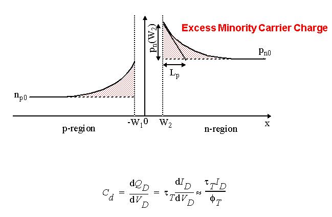
10 Diffusion Capacitance
11 I D (A) Secondary Effects V D (V) Avalanche Breakdown

12 Diode Model R S + V D - I D C D
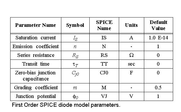
13 SPICE Parameters
14 What is a Transistor? A Switch! An MOS Transistor V GS V T V GS S R on D

15 The MOS Transistor Polysilicon Aluminum

16 MOS Transistors - Types and Symbols D D G G S NMOS Enhancement D NMOS S Depletion D G G B PMOS S Enhancement S NMOS with Bulk Contact
17 Threshold Voltage: Concept S - V GS + G D n+ n+ n-channel p-substrate Depletion Region B

18 The Threshold Voltage
19 The Body Effect V T (V) V BS (V)
20 I D (A) Current-Voltage Relations A good ol transistor -4 x 10 6 VGS= 2.5 V 5 4 Resistive Saturation VGS= 2.0 V 3 2 V DS = V GS - V T VGS= 1.5 V Quadratic Relationship 1 VGS= 1.0 V V DS (V)
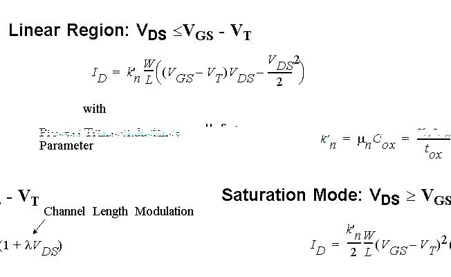
21 Transistor in Linear S V GS G V DS D I D n + V(x) + n + L x p-substrate B MOS transistor and its bias conditions

22 Transistor in Saturation V GS G V DS > V GS - V T S D n+ - V GS - V T + n+ Pinch-off


23 Current-Voltage Relations Long-Channel Device

24 A model for manual analysis
25 I D (A) Current-Voltage Relations The Deep-Submicron Era 2.5 x Early Saturation VGS= 2.5 V 1.5 VGS= 2.0 V 1 VGS= 1.5 V Linear Relationship 0.5 VGS= 1.0 V V DS (V)
26 u n (m/s) Velocity Saturation u sat = 10 5 Constant velocity Constant mobility (slope = µ) c = 1.5 (V/µm)
27 Perspective I D Long-channel device V GS = V DD Short-channel device V DSAT V GS - V T V DS
28 I D (A) I D (A) I D versus V GS 6 x x quadratic linear V GS (V) Long Channel 0.5 quadratic V GS (V) Short Channel
29 I D (A) I D (A) I D versus V DS 6 x VGS= 2.5 V Resistive Saturation VGS= 2.0 V x 10 VGS= 2.5 V VGS= 2.0 V 3 2 V DS = V GS - V T VGS= 1.5 V 1 VGS= 1.5 V 1 VGS= 1.0 V 0.5 VGS= 1.0 V V DS (V) Long Channel V DS (V) Short Channel


30 A unified model for manual analysis G S D B
31 I D (A) Simple Model versus SPICE 2.5 x 10⁻⁴ V DS =V DSAT Velocity Saturated Linear V DSAT =V GT V DS =V GT Saturated V DS (V)
32 I D (A) A PMOS Transistor 0 x 10-4 VGS = -1.0V -0.2 VGS = -1.5V VGS = -2.0V VGS = -2.5V Assume all variables negative! V DS (V)

33 Transistor Model for Manual Analysis
34 The Transistor as a Switch V GS V T S R on I D D V GS = V DD R mid R 0 V DD /2 V DD V DS
35 The Transistor as a Switch

36 The Transistor as a Switch
37 MOS Capacitances Dynamic Behavior
38 Dynamic Behavior of MOS Transistor G C GS C GD S D C SB C GB C DB B
39 The Gate Capacitance Polysilicon gate Source n + x d x d W Drain n + L d Top view Gate-bulk overlap t ox Gate oxide n + L n + Cross section

40 Gate Capacitance G G G S C GC C GC C GC D S D S D Cut-off Resistive Saturation Most important regions in digital design: saturation and cut-off
41 Gate Capacitance WLC ox C GC WLC ox C GC 2WLC ox WLC ox 2 C GC B C GCS = C GCD WLC ox 2 C GCS C GCD 3 V GS 0 V DS /(V GS -V T ) 1 Capacitance as a function of VGS (with VDS = 0) Capacitance as a function of the degree of saturation

42 Gate Capacitance (F) Measuring the Gate Cap I V GS V GS (V)
43 Diffusion Capacitance Channel-stop implant N A 1 Side wall W Source N D Bottom x j L S Side wall Substrate N A Channel
44 Junction Capacitance


45 Linearizing the Junction Capacitance Replace non-linear capacitance by large-signal equivalent linear capacitance which displaces equal charge over voltage swing of interest

46 Capacitances in 0.25 mm CMOS process
47 The Sub-Micron MOS Transistor Threshold Variations Subthreshold Conduction Parasitic Resistances
48 Threshold Variations V T V T Long-channel threshold Low V DS threshold Threshold as a function of the length (for low V DS ) L V DS Drain-induced barrier lowering (for low L)

 Typical values for S: 60.")
49 I D (A) Sub-Threshold Conduction Linear The Slope Factor I D ~ I 0 e qv nkt GS, n 1 C C D ox Quadratic S is DV GS for I D2 /I D1 = Exponential V T V GS (V) Typical values for S: mv/decade

50 Sub-Threshold I D vs V GS qvgs nkt I D I0e 1 e qv kt DS V DS from 0 to 0.5V

51 Sub-Threshold I D vs V DS I D I 0 e qv nkt GS 1 e qv kt DS 1 V DS V GS from 0 to 0.3V
 V DS V DSAT Weak Inversion (Sub-Threshold) V GS V T Exponential in V GS with linear V DS")
52 Summary of MOSFET Operating Regions Strong Inversion V GS > V T Linear (Resistive) V DS < V DSAT Saturated (Constant Current) V DS V DSAT Weak Inversion (Sub-Threshold) V GS V T Exponential in V GS with linear V DS dependence
53 Parasitic Resistances G Polysilicon gate L D Drain contact V GS,eff S D W R S R D Drain
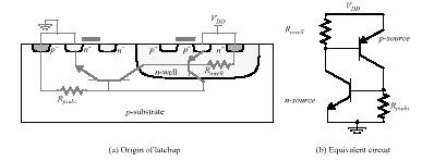
54 Latch-up

55 Future Perspectives 25 nm FINFET MOS transistor
Digital Integrated Circuits A Design Perspective. Jan M. Rabaey Anantha Chandrakasan Borivoje Nikolic. The Devices. July 30, Devices.
 Digital Integrated Circuits A Design Perspective Jan M. Rabaey Anantha Chandrakasan Borivoje Nikolic The July 30, 2002 1 Goal of this chapter Present intuitive understanding of device operation Introduction
The Devices. Digital Integrated Circuits A Design Perspective. Jan M. Rabaey Anantha Chandrakasan Borivoje Nikolic. July 30, 2002
 igital Integrated Circuits A esign Perspective Jan M. Rabaey Anantha Chandrakasan Borivoje Nikolic The evices July 30, 2002 Goal of this chapter Present intuitive understanding of device operation Introduction
Device Models (PN Diode, MOSFET )
") Device Models (PN Diode, MOSFET ) Instructor: Steven P. Levitan steve@ece.pitt.edu TA: Gayatri Mehta, José Martínez Book: Digital Integrated Circuits: A Design Perspective; Jan Rabaey Lab Notes: Handed
Device Models (PN Diode, MOSFET ) Instructor: Steven P. Levitan steve@ece.pitt.edu TA: Gayatri Mehta, José Martínez Book: Digital Integrated Circuits: A Design Perspective; Jan Rabaey Lab Notes: Handed
CMOS INVERTER. Last Lecture. Metrics for qualifying digital circuits. »Cost» Reliability» Speed (delay)»performance
»performance") CMOS INVERTER Last Lecture Metrics for qualifying digital circuits»cost» Reliability» Speed (delay)»performance 1 Today s lecture The CMOS inverter at a glance An MOS transistor model for manual analysis
CMOS INVERTER Last Lecture Metrics for qualifying digital circuits»cost» Reliability» Speed (delay)»performance 1 Today s lecture The CMOS inverter at a glance An MOS transistor model for manual analysis
The Devices. Jan M. Rabaey
 The Devices Jan M. Rabaey Goal of this chapter Present intuitive understanding of device operation Introduction of basic device equations Introduction of models for manual analysis Introduction of models
Today s lecture. EE141- Spring 2003 Lecture 4. Design Rules CMOS Inverter MOS Transistor Model
 - Spring 003 Lecture 4 Design Rules CMOS Inverter MOS Transistor Model Today s lecture Design Rules The CMOS inverter at a glance An MOS transistor model for manual analysis Important! Labs start next
CMPEN 411 VLSI Digital Circuits. Lecture 03: MOS Transistor
 CMPEN 411 VLSI Digital Circuits Lecture 03: MOS Transistor Kyusun Choi [Adapted from Rabaey s Digital Integrated Circuits, Second Edition, 2003 J. Rabaey, A. Chandrakasan, B. Nikolic] CMPEN 411 L03 S.1
Lecture 4: CMOS Transistor Theory
 Introduction to CMOS VLSI Design Lecture 4: CMOS Transistor Theory David Harris, Harvey Mudd College Kartik Mohanram and Steven Levitan University of Pittsburgh Outline q Introduction q MOS Capacitor q
The Devices: MOS Transistors
 The Devices: MOS Transistors References: Semiconductor Device Fundamentals, R. F. Pierret, Addison-Wesley Digital Integrated Circuits: A Design Perspective, J. Rabaey et.al. Prentice Hall NMOS Transistor
MOSFET: Introduction
 E&CE 437 Integrated VLSI Systems MOS Transistor 1 of 30 MOSFET: Introduction Metal oxide semiconductor field effect transistor (MOSFET) or MOS is widely used for implementing digital designs Its major
Integrated Circuits & Systems
 Federal University of Santa Catarina Center for Technology Computer Science & Electronics Engineering Integrated Circuits & Systems INE 5442 Lecture 10 MOSFET part 1 guntzel@inf.ufsc.br ual-well Trench-Isolated
EE5311- Digital IC Design
 EE5311- Digital IC Design Module 1 - The Transistor Janakiraman V Assistant Professor Department of Electrical Engineering Indian Institute of Technology Madras Chennai October 28, 2017 Janakiraman, IITM
EE115C Winter 2017 Digital Electronic Circuits. Lecture 3: MOS RC Model, CMOS Manufacturing
 EE115C Winter 2017 Digital Electronic Circuits Lecture 3: MOS RC Model, CMOS Manufacturing Agenda MOS Transistor: RC Model (pp. 104-113) S R on D CMOS Manufacturing Process (pp. 36-46) S S C GS G G C GD
MOS Transistor I-V Characteristics and Parasitics
 ECEN454 Digital Integrated Circuit Design MOS Transistor I-V Characteristics and Parasitics ECEN 454 Facts about Transistors So far, we have treated transistors as ideal switches An ON transistor passes
Check course home page periodically for announcements. Homework 2 is due TODAY by 5pm In 240 Cory
 EE141 Fall 005 Lecture 6 MOS Capacitances, Propagation elay Important! Check course home page periodically for announcements Homework is due TOAY by 5pm In 40 Cory Homework 3 will be posted TOAY ue Thursday
The Devices. Devices
 The The MOS Transistor Gate Oxyde Gate Source n+ Polysilicon Drain n+ Field-Oxyde (SiO 2 ) p-substrate p+ stopper Bulk Contact CROSS-SECTION of NMOS Transistor Cross-Section of CMOS Technology MOS transistors
Important! EE141- Fall 2002 Lecture 5. CMOS Inverter MOS Transistor Model
 - Fall 00 Lecture 5 CMO Inverter MO Transistor Model Important! Lab 3 this week You must show up in one of the lab sessions this week If you don t show up you will be dropped from the class» Unless you
B.Supmonchai June 26, q Introduction of device basic equations. q Introduction of models for manual analysis.
 June 26, 2004 oal of this chapter Chapter 2 MO Transistor Theory oonchuay upmonchai Integrated esign Application Research (IAR) Laboratory June 16th, 2004; Revised June 16th, 2005 q Present intuitive understanding
Lecture 3: CMOS Transistor Theory
 Lecture 3: CMOS Transistor Theory Outline Introduction MOS Capacitor nmos I-V Characteristics pmos I-V Characteristics Gate and Diffusion Capacitance 2 Introduction So far, we have treated transistors
Announcements. EE141- Fall 2002 Lecture 7. MOS Capacitances Inverter Delay Power
 - Fall 2002 Lecture 7 MOS Capacitances Inverter Delay Power Announcements Wednesday 12-3pm lab cancelled Lab 4 this week Homework 2 due today at 5pm Homework 3 posted tonight Today s lecture MOS capacitances
MOS Transistor Properties Review
 MOS Transistor Properties Review 1 VLSI Chip Manufacturing Process Photolithography: transfer of mask patterns to the chip Diffusion or ion implantation: selective doping of Si substrate Oxidation: SiO
HW 5 posted due in two weeks Lab this week Midterm graded Project to be launched in week 7
 HW 5 posted due in two weeks Lab this week Midterm graded Project to be launched in week 7 2 What do digital IC designers need to know? 5 EE4 EECS4 6 3 0< V GS - V T < V DS Pinch-off 7 For (V GS V T )
Lecture 04 Review of MOSFET
 ECE 541/ME 541 Microelectronic Fabrication Techniques Lecture 04 Review of MOSFET Zheng Yang (ERF 3017, email: yangzhen@uic.edu) What is a Transistor? A Switch! An MOS Transistor V GS V T V GS S Ron D
EE105 Fall 2014 Microelectronic Devices and Circuits. NMOS Transistor Capacitances: Saturation Region
 EE105 Fall 014 Microelectronic Devices and Circuits Prof. Ming C. Wu wu@eecs.berkeley.edu 511 Sutardja Dai Hall (SDH) 1 NMOS Transistor Capacitances: Saturation Region Drain no longer connected to channel
ECE 342 Electronic Circuits. 3. MOS Transistors
 ECE 342 Electronic Circuits 3. MOS Transistors Jose E. Schutt-Aine Electrical & Computer Engineering University of Illinois jschutt@emlab.uiuc.edu 1 NMOS Transistor Typically L = 0.1 to 3 m, W = 0.2 to
Practice 3: Semiconductors
 Practice 3: Semiconductors Digital Electronic Circuits Semester A 2012 VLSI Fabrication Process VLSI Very Large Scale Integration The ability to fabricate many devices on a single substrate within a given
Chapter 2 CMOS Transistor Theory. Jin-Fu Li Department of Electrical Engineering National Central University Jungli, Taiwan
 Chapter 2 CMOS Transistor Theory Jin-Fu Li Department of Electrical Engineering National Central University Jungli, Taiwan Outline Introduction MOS Device Design Equation Pass Transistor Jin-Fu Li, EE,
EEC 118 Lecture #2: MOSFET Structure and Basic Operation. Rajeevan Amirtharajah University of California, Davis Jeff Parkhurst Intel Corporation
 EEC 118 Lecture #2: MOSFET Structure and Basic Operation Rajeevan Amirtharajah University of California, Davis Jeff Parkhurst Intel Corporation Announcements Lab 1 this week, report due next week Bring
CMPEN 411 VLSI Digital Circuits. Lecture 04: CMOS Inverter (static view)
") CMPEN 411 VLSI Digital Circuits Lecture 04: CMOS Inverter (static view) Kyusun Choi [Adapted from Rabaey s Digital Integrated Circuits, Second Edition, 2003 J. Rabaey, A. Chandrakasan, B. Nikolic] CMPEN
CMPEN 411 VLSI Digital Circuits Lecture 04: CMOS Inverter (static view) Kyusun Choi [Adapted from Rabaey s Digital Integrated Circuits, Second Edition, 2003 J. Rabaey, A. Chandrakasan, B. Nikolic] CMPEN
EE105 - Fall 2006 Microelectronic Devices and Circuits
 EE105 - Fall 2006 Microelectronic Devices and Circuits Prof. Jan M. Rabaey (jan@eecs) Lecture 7: MOS Transistor Some Administrative Issues Lab 2 this week Hw 2 due on We Hw 3 will be posted same day MIDTERM
MOS Transistor Theory
 MOS Transistor Theory So far, we have viewed a MOS transistor as an ideal switch (digital operation) Reality: less than ideal EE 261 Krish Chakrabarty 1 Introduction So far, we have treated transistors
MOS Transistors. Prof. Krishna Saraswat. Department of Electrical Engineering Stanford University Stanford, CA
 MOS Transistors Prof. Krishna Saraswat Department of Electrical Engineering S Stanford, CA 94305 saraswat@stanford.edu 1 1930: Patent on the Field-Effect Transistor! Julius Lilienfeld filed a patent describing
ECE 497 JS Lecture - 12 Device Technologies
 ECE 497 JS Lecture - 12 Device Technologies Spring 2004 Jose E. Schutt-Aine Electrical & Computer Engineering University of Illinois jose@emlab.uiuc.edu 1 NMOS Transistor 2 ρ Source channel charge density
VLSI Design I; A. Milenkovic 1
 Review: implified CMO Inverter Process CPE/EE 7, CPE 7 VLI esign I L: MO Transistor cut line epartment of Electrical and Computer Engineering University of Alabama in Huntsville Aleksandar Milenkovic (
MOS Transistor Theory
 CHAPTER 3 MOS Transistor Theory Outline 2 1. Introduction 2. Ideal I-V Characteristics 3. Nonideal I-V Effects 4. C-V Characteristics 5. DC Transfer Characteristics 6. Switch-level RC Delay Models MOS
ESE 570: Digital Integrated Circuits and VLSI Fundamentals
 ESE 570: Digital Integrated Circuits and VLSI Fundamentals Lec 7: February 4, 2016 MOS SPICE Models, MOS Parasitic Details Lecture Outline! MOS Capacitances " Extrinsic " Intrinsic! Lumped Capacitance
Lecture 15: MOS Transistor models: Body effects, SPICE models. Context. In the last lecture, we discussed the modes of operation of a MOS FET:
 Lecture 15: MOS Transistor models: Body effects, SPICE models Context In the last lecture, we discussed the modes of operation of a MOS FET: oltage controlled resistor model I- curve (Square-Law Model)
Course Administration. CPE/EE 427, CPE 527 VLSI Design I L04: MOS Transistors. Review: CMOS Process at a Glance
 Course Administration CPE/EE 7, CPE 7 VLI esign I L: MO Transistors epartment of Electrical and Computer Engineering University of Alabama in Huntsville Aleksandar Milenkovic ( www.ece.uah.edu/~milenka
Lecture 5: CMOS Transistor Theory
 Lecture 5: CMOS Transistor Theory Slides courtesy of Deming Chen Slides based on the initial set from David Harris CMOS VLSI Design Outline q q q q q q q Introduction MOS Capacitor nmos I-V Characteristics
EE105 - Fall 2005 Microelectronic Devices and Circuits
 EE105 - Fall 005 Microelectronic Devices and Circuits ecture 7 MOS Transistor Announcements Homework 3, due today Homework 4 due next week ab this week Reading: Chapter 4 1 ecture Material ast lecture
! MOS Capacitances. " Extrinsic. " Intrinsic. ! Lumped Capacitance Model. ! First Order Capacitor Summary. ! Capacitance Implications
 ESE 570: Digital Integrated Circuits and VLSI Fundamentals Lec 7: February, 07 MOS SPICE Models, MOS Parasitic Details Lecture Outline! MOS Capacitances " Extrinsic " Intrinsic! Lumped Capacitance Model!
Chapter 4 Field-Effect Transistors
 Chapter 4 Field-Effect Transistors Microelectronic Circuit Design Richard C. Jaeger Travis N. Blalock 5/5/11 Chap 4-1 Chapter Goals Describe operation of MOSFETs. Define FET characteristics in operation
VLSI Design The MOS Transistor
 VLSI Design The MOS Transistor Frank Sill Torres Universidade Federal de Minas Gerais (UFMG), Brazil VLSI Design: CMOS Technology 1 Outline Introduction MOS Capacitor nmos I-V Characteristics pmos I-V
ESE 570: Digital Integrated Circuits and VLSI Fundamentals
 ESE 570: Digital Integrated Circuits and VLSI Fundamentals Lec 5: January 25, 2018 MOS Operating Regions, pt. 1 Lecture Outline! 3 Regions of operation for MOSFET " Subthreshold " Linear " Saturation!
EE 560 MOS TRANSISTOR THEORY PART 2. Kenneth R. Laker, University of Pennsylvania
 1 EE 560 MOS TRANSISTOR THEORY PART nmos TRANSISTOR IN LINEAR REGION V S = 0 V G > V T0 channel SiO V D = small 4 C GC C BC substrate depletion region or bulk B p nmos TRANSISTOR AT EDGE OF SATURATION
Lecture 12: MOSFET Devices
 Lecture 12: MOSFET Devices Gu-Yeon Wei Division of Engineering and Applied Sciences Harvard University guyeon@eecs.harvard.edu Wei 1 Overview Reading S&S: Chapter 5.1~5.4 Supplemental Reading Background
ECE 342 Electronic Circuits. Lecture 6 MOS Transistors
 ECE 342 Electronic Circuits Lecture 6 MOS Transistors Jose E. Schutt-Aine Electrical & Computer Engineering University of Illinois jesa@illinois.edu 1 NMOS Transistor Typically L = 0.1 to 3 m, W = 0.2
VLSI Design and Simulation
 VLSI Design and Simulation Performance Characterization Topics Performance Characterization Resistance Estimation Capacitance Estimation Inductance Estimation Performance Characterization Inverter Voltage
CMOS Inverter (static view)
") Review: Design Abstraction Levels SYSTEM CMOS Inverter (static view) + MODULE GATE [Adapted from Chapter 5. 5.3 CIRCUIT of G DEVICE Rabaey s Digital Integrated Circuits,, J. Rabaey et al.] S D Review:
Review: Design Abstraction Levels SYSTEM CMOS Inverter (static view) + MODULE GATE [Adapted from Chapter 5. 5.3 CIRCUIT of G DEVICE Rabaey s Digital Integrated Circuits,, J. Rabaey et al.] S D Review:
Lecture 11: MOS Transistor
 Lecture 11: MOS Transistor Prof. Niknejad Lecture Outline Review: MOS Capacitors Regions MOS Capacitors (3.8 3.9) CV Curve Threshold Voltage MOS Transistors (4.1 4.3): Overview Cross-section and layout
The Inverter. Digital Integrated Circuits A Design Perspective. Jan M. Rabaey Anantha Chandrakasan Borivoje Nikolic
 Digital Integrated Circuits A Design Perspective Jan M. Rabaey Anantha Chandrakasan Borivoje Nikolic The Inverter Revised from Digital Integrated Circuits, Jan M. Rabaey el, 2003 Propagation Delay CMOS
Digital Integrated Circuits
 Chapter 6 The CMOS Inverter 1 Contents Introduction (MOST models) 0, 1 st, 2 nd order The CMOS inverter : The static behavior: o DC transfer characteristics, o Short-circuit current The CMOS inverter :
Introduction and Background
 Analog CMOS Integrated Circuit Design Introduction and Background Dr. Jawdat Abu-Taha Department of Electrical and Computer Engineering Islamic University of Gaza jtaha@iugaza.edu.ps 1 Marking Assignments
Quantitative MOSFET. Step 1. Connect the MOS capacitor results for the electron charge in the inversion layer Q N to the drain current.
 Quantitative MOSFET Step 1. Connect the MOS capacitor results for the electron charge in the inversion layer Q N to the drain current. V DS _ n source polysilicon gate y = y * 0 x metal interconnect to
ECE 546 Lecture 10 MOS Transistors
 ECE 546 Lecture 10 MOS Transistors Spring 2018 Jose E. Schutt-Aine Electrical & Computer Engineering University of Illinois jesa@illinois.edu NMOS Transistor NMOS Transistor N-Channel MOSFET Built on p-type
FIELD-EFFECT TRANSISTORS
 FIEL-EFFECT TRANSISTORS 1 Semiconductor review 2 The MOS capacitor 2 The enhancement-type N-MOS transistor 3 I-V characteristics of enhancement MOSFETS 4 The output characteristic of the MOSFET in saturation
LECTURE 3 MOSFETS II. MOS SCALING What is Scaling?
 LECTURE 3 MOSFETS II Lecture 3 Goals* * Understand constant field and constant voltage scaling and their effects. Understand small geometry effects for MOS transistors and their implications modeling and
EE 560 MOS TRANSISTOR THEORY
 1 EE 560 MOS TRANSISTOR THEORY PART 1 TWO TERMINAL MOS STRUCTURE V G (GATE VOLTAGE) 2 GATE OXIDE SiO 2 SUBSTRATE p-type doped Si (N A = 10 15 to 10 16 cm -3 ) t ox V B (SUBSTRATE VOLTAGE) EQUILIBRIUM:
Lecture 11: MOSFET Modeling
 Digital Integrated Circuits (83-313) Lecture 11: MOSFET ing Semester B, 2016-17 Lecturer: Dr. Adam Teman TAs: Itamar Levi, Robert Giterman 18 June 2017 Disclaimer: This course was prepared, in its entirety,
Lecture 12: MOS Capacitors, transistors. Context
 Lecture 12: MOS Capacitors, transistors Context In the last lecture, we discussed PN diodes, and the depletion layer into semiconductor surfaces. Small signal models In this lecture, we will apply those
ECE-305: Fall 2017 MOS Capacitors and Transistors
 ECE-305: Fall 2017 MOS Capacitors and Transistors Pierret, Semiconductor Device Fundamentals (SDF) Chapters 15+16 (pp. 525-530, 563-599) Professor Peter Bermel Electrical and Computer Engineering Purdue
MOS Transistor Theory MOSFET Symbols Current Characteristics of MOSFET. MOS Symbols and Characteristics. nmos Enhancement Transistor
 MOS Transistor Theory MOSFET Symbols Current Characteristics of MOSFET Calculation of t and Important 2 nd Order Effects SmallSignal Signal MOSFET Model Summary Material from: CMOS LSI Design By Weste
Introduction to CMOS VLSI. Chapter 2: CMOS Transistor Theory. Harris, 2004 Updated by Li Chen, Outline
 Introduction to MOS VLSI Design hapter : MOS Transistor Theory copyright@david Harris, 004 Updated by Li hen, 010 Outline Introduction MOS apacitor nmos IV haracteristics pmos IV haracteristics Gate and
Lecture 10 MOSFET (III) MOSFET Equivalent Circuit Models
 MOSFET Equivalent Circuit Models") Lecture 10 MOSFET (III) MOSFET Equivalent Circuit Models Outline Lowfrequency smallsignal equivalent circuit model Highfrequency smallsignal equivalent circuit model Reading Assignment: Howe and Sodini;
Lecture 10 MOSFET (III) MOSFET Equivalent Circuit Models Outline Lowfrequency smallsignal equivalent circuit model Highfrequency smallsignal equivalent circuit model Reading Assignment: Howe and Sodini;
MOSFET Physics: The Long Channel Approximation
 MOSFET Physics: The ong Channel Approximation A basic n-channel MOSFET (Figure 1) consists of two heavily-doped n-type regions, the Source and Drain, that comprise the main terminals of the device. The
Operation and Modeling of. The MOS Transistor. Second Edition. Yannis Tsividis Columbia University. New York Oxford OXFORD UNIVERSITY PRESS
 Operation and Modeling of The MOS Transistor Second Edition Yannis Tsividis Columbia University New York Oxford OXFORD UNIVERSITY PRESS CONTENTS Chapter 1 l.l 1.2 1.3 1.4 1.5 1.6 1.7 Chapter 2 2.1 2.2
! PN Junction. ! MOS Transistor Topology. ! Threshold. ! Operating Regions. " Resistive. " Saturation. " Subthreshold (next class)
") ESE370: ircuitlevel Modeling, Design, and Optimization for Digital Systems Lec 7: September 20, 2017 MOS Transistor Operating Regions Part 1 Today! PN Junction! MOS Transistor Topology! Threshold! Operating
ESE370: ircuitlevel Modeling, Design, and Optimization for Digital Systems Lec 7: September 20, 2017 MOS Transistor Operating Regions Part 1 Today! PN Junction! MOS Transistor Topology! Threshold! Operating
Lecture 10 MOSFET (III) MOSFET Equivalent Circuit Models
 MOSFET Equivalent Circuit Models") Lecture 1 MOSFET (III) MOSFET Equivalent Circuit Models Outline Lowfrequency smallsignal equivalent circuit model Highfrequency smallsignal equivalent circuit model Reading Assignment: Howe and Sodini;
Lecture 1 MOSFET (III) MOSFET Equivalent Circuit Models Outline Lowfrequency smallsignal equivalent circuit model Highfrequency smallsignal equivalent circuit model Reading Assignment: Howe and Sodini;
Long-channel MOSFET IV Corrections
 Long-channel MOSFET IV orrections Three MITs of the Day The body ect and its influence on long-channel V th. Long-channel subthreshold conduction and control (subthreshold slope S) Scattering components
Lecture 29 - The Long Metal-Oxide-Semiconductor Field-Effect Transistor (cont.) April 20, 2007
 April 20, 2007") 6.720J/3.43J - Integrated Microelectronic Devices - Spring 2007 Lecture 29-1 Lecture 29 - The Long Metal-Oxide-Semiconductor Field-Effect Transistor (cont.) April 20, 2007 Contents: 1. Non-ideal and second-order
6.720J/3.43J - Integrated Microelectronic Devices - Spring 2007 Lecture 29-1 Lecture 29 - The Long Metal-Oxide-Semiconductor Field-Effect Transistor (cont.) April 20, 2007 Contents: 1. Non-ideal and second-order
Section 12: Intro to Devices
 Section 12: Intro to Devices Extensive reading materials on reserve, including Robert F. Pierret, Semiconductor Device Fundamentals EE143 Ali Javey Bond Model of Electrons and Holes Si Si Si Si Si Si Si
ECEN474/704: (Analog) VLSI Circuit Design Spring 2018
 VLSI Circuit Design Spring 2018") ECEN474/704: (Analog) SI Circuit Design Spring 2018 ecture 2: MOS ransistor Modeling Sam Palermo Analog & Mixed-Signal Center exas A&M University Announcements If you haven t already, turn in your 0.18um
ECEN474/704: (Analog) SI Circuit Design Spring 2018 ecture 2: MOS ransistor Modeling Sam Palermo Analog & Mixed-Signal Center exas A&M University Announcements If you haven t already, turn in your 0.18um
Microelectronics Part 1: Main CMOS circuits design rules
 GBM8320 Dispositifs Médicaux telligents Microelectronics Part 1: Main CMOS circuits design rules Mohamad Sawan et al. Laboratoire de neurotechnologies Polystim! http://www.cours.polymtl.ca/gbm8320/! med-amine.miled@polymtl.ca!
Scaling Issues in Planar FET: Dual Gate FET and FinFETs
 Scaling Issues in Planar FET: Dual Gate FET and FinFETs Lecture 12 Dr. Amr Bayoumi Fall 2014 Advanced Devices (EC760) Arab Academy for Science and Technology - Cairo 1 Outline Scaling Issues for Planar
EECS130 Integrated Circuit Devices
 EECS130 Integrated Circuit Devices Professor Ali Javey 10/30/2007 MOSFETs Lecture 4 Reading: Chapter 17, 19 Announcements The next HW set is due on Thursday. Midterm 2 is next week!!!! Threshold and Subthreshold
Fundamentals of the Metal Oxide Semiconductor Field-Effect Transistor
 Triode Working FET Fundamentals of the Metal Oxide Semiconductor Field-Effect Transistor The characteristics of energy bands as a function of applied voltage. Surface inversion. The expression for the
ESE 570: Digital Integrated Circuits and VLSI Fundamentals
 ESE 570: Digital Integrated Circuits and VLSI Fundamentals Lec 4: January 23, 2018 MOS Transistor Theory, MOS Model Penn ESE 570 Spring 2018 Khanna Lecture Outline! CMOS Process Enhancements! Semiconductor
ENGR890 Digital VLSI Design Fall Lecture 4: CMOS Inverter (static view)
") ENGR89 Digital VLSI Design Fall 5 Lecture 4: CMOS Inverter (static view) [Adapted from Chapter 5 of Digital Integrated Circuits, 3, J. Rabaey et al.] [Also borrowed from Vijay Narayanan and Mary Jane Irwin]
ENGR89 Digital VLSI Design Fall 5 Lecture 4: CMOS Inverter (static view) [Adapted from Chapter 5 of Digital Integrated Circuits, 3, J. Rabaey et al.] [Also borrowed from Vijay Narayanan and Mary Jane Irwin]
Semiconductor Physics fall 2012 problems
 Semiconductor Physics fall 2012 problems 1. An n-type sample of silicon has a uniform density N D = 10 16 atoms cm -3 of arsenic, and a p-type silicon sample has N A = 10 15 atoms cm -3 of boron. For each
MOSFET Capacitance Model
 MOSFET Capacitance Model So far we discussed the MOSFET DC models. In real circuit operation, the device operates under time varying terminal voltages and the device operation can be described by: 1 small
Nanoscale CMOS Design Issues
 Nanoscale CMOS Design Issues Jaydeep P. Kulkarni Assistant Professor, ECE Department The University of Texas at Austin jaydeep@austin.utexas.edu Fall, 2017, VLSI-1 Class Transistor I-V Review Agenda Non-ideal
Lecture Outline. ESE 570: Digital Integrated Circuits and VLSI Fundamentals. Review: MOS Capacitor with External Bias
 ESE 57: Digital Integrated Circuits and VLSI Fundamentals Lec 5: Januar 6, 17 MOS Operating Regions, pt. 1 Lecture Outline! 3 Regions of operation for MOSFET " Subthreshold " Linear " Saturation! Level
Metal-oxide-semiconductor field effect transistors (2 lectures)
") Metal-ide-semiconductor field effect transistors ( lectures) MOS physics (brief in book) Current-voltage characteristics - pinch-off / channel length modulation - weak inversion - velocity saturation -
Metal-ide-semiconductor field effect transistors ( lectures) MOS physics (brief in book) Current-voltage characteristics - pinch-off / channel length modulation - weak inversion - velocity saturation -
Technische Universität Graz. Institute of Solid State Physics. 11. MOSFETs
 Technische Universität Graz Institute of Solid State Physics 11. MOSFETs Dec. 12, 2018 Gradual channel approximation accumulation depletion inversion http://lampx.tugraz.at/~hadley/psd/l10/gradualchannelapprox.php
EEC 116 Lecture #3: CMOS Inverters MOS Scaling. Rajeevan Amirtharajah University of California, Davis Jeff Parkhurst Intel Corporation
 EEC 116 Lecture #3: CMOS Inverters MOS Scaling Rajeevan Amirtharajah University of California, Davis Jeff Parhurst Intel Corporation Outline Review: Inverter Transfer Characteristics Lecture 3: Noise Margins,
Chapter 5 MOSFET Theory for Submicron Technology
 Chapter 5 MOSFET Theory for Submicron Technology Short channel effects Other small geometry effects Parasitic components Velocity saturation/overshoot Hot carrier effects ** Majority of these notes are
MOSFET. Id-Vd curve. I DS Transfer curve V G. Lec. 8. Vd=1V. Saturation region. V Th
 MOSFET Id-Vd curve Saturation region I DS Transfer curve Vd=1V V Th V G 1 0 < V GS < V T V GS > V T V Gs >V T & Small V D > 0 I DS WQ inv WC v WC i V V VDS V V G i T G n T L n I D g V D (g conductance
ESE370: Circuit-Level Modeling, Design, and Optimization for Digital Systems. Today. Refinement. Last Time. No Field. Body Contact
 ESE370: Circuit-Level Modeling, Design, and Optimization for Digital Systems Day 10: September 6, 01 MOS Transistor Basics Today MOS Transistor Topology Threshold Operating Regions Resistive Saturation
EE382M-14 CMOS Analog Integrated Circuit Design
 EE382M-14 CMOS Analog Integrated Circuit Design Lecture 3, MOS Capacitances, Passive Components, and Layout of Analog Integrated Circuits MOS Capacitances Type of MOS transistor capacitors Depletion capacitance
2.CMOS Transistor Theory
 MOS VLSI esign 2.MOS Transistor Theory Fu yuzhuo School of microelectronics,sjtu Introduction outline P junction principle MOS transistor introduction Ideal I-V characteristics under static conditions
University of Pennsylvania Department of Electrical Engineering. ESE 570 Midterm Exam March 14, 2013 FORMULAS AND DATA
 University of Pennsylvania Department of Electrical Engineering ESE 570 Midterm Exam March 4, 03 FORMULAS AND DATA. PHYSICAL CONSTANTS: n i = intrinsic concentration undoped) silicon =.45 x 0 0 cm -3 @
The Physical Structure (NMOS)
") The Physical Structure (NMOS) Al SiO2 Field Oxide Gate oxide S n+ Polysilicon Gate Al SiO2 SiO2 D n+ L channel P Substrate Field Oxide contact Metal (S) n+ (G) L W n+ (D) Poly 1 Transistor Resistance Two
The Physical Structure (NMOS) Al SiO2 Field Oxide Gate oxide S n+ Polysilicon Gate Al SiO2 SiO2 D n+ L channel P Substrate Field Oxide contact Metal (S) n+ (G) L W n+ (D) Poly 1 Transistor Resistance Two
ECE321 Electronics I
 EE31 Electronics I Lecture 8: MOSET Threshold Voltage and Parasitic apacitances Payman Zarkesh-Ha Office: EE Bldg. 3B Office hours: Tuesday :-3:PM or by appointment E-mail: payman@ece.unm.edu Slide: 1
and V DS V GS V T (the saturation region) I DS = k 2 (V GS V T )2 (1+ V DS )
 I DS = k 2 (V GS V T )2 (1+ V DS )") ECE 4420 Spring 2005 Page 1 FINAL EXAMINATION NAME SCORE /100 Problem 1O 2 3 4 5 6 7 Sum Points INSTRUCTIONS: This exam is closed book. You are permitted four sheets of notes (three of which are your sheets
ECE 4420 Spring 2005 Page 1 FINAL EXAMINATION NAME SCORE /100 Problem 1O 2 3 4 5 6 7 Sum Points INSTRUCTIONS: This exam is closed book. You are permitted four sheets of notes (three of which are your sheets
Lecture 210 Physical Aspects of ICs (12/15/01) Page 210-1
 Page 210-1") Lecture 210 Physical Aspects of ICs (12/15/01) Page 210-1 LECTURE 210 PHYSICAL ASPECTS OF ICs (READING: Text-Sec. 2.5, 2.6, 2.8) INTRODUCTION Objective Illustrate the physical aspects of integrated circuits
Lecture 210 Physical Aspects of ICs (12/15/01) Page 210-1 LECTURE 210 PHYSICAL ASPECTS OF ICs (READING: Text-Sec. 2.5, 2.6, 2.8) INTRODUCTION Objective Illustrate the physical aspects of integrated circuits
ESE 570: Digital Integrated Circuits and VLSI Fundamentals
 ESE 570: Digital Integrated Circuits and VLSI Fundamentals Lec 6: January 30, 2018 MOS Operating Regions, pt. 2 Lecture Outline! Operating Regions (review) " Subthreshold " Resistive " Saturation! Intro.
P. R. Nelson 1 ECE418 - VLSI. Midterm Exam. Solutions
 P. R. Nelson 1 ECE418 - VLSI Midterm Exam Solutions 1. (8 points) Draw the cross-section view for A-A. The cross-section view is as shown below.. ( points) Can you tell which of the metal1 regions is the
Final Examination EE 130 December 16, 1997 Time allotted: 180 minutes
 Final Examination EE 130 December 16, 1997 Time allotted: 180 minutes Problem 1: Semiconductor Fundamentals [30 points] A uniformly doped silicon sample of length 100µm and cross-sectional area 100µm 2
Step 1. Finding V M. Goal: Þnd V M = input voltage for the output = V M both transistors are saturated at V IN = V M since
 Step 1. Finding V M Goal: Þnd V M = input voltage for the output = V M both transistors are saturated at V IN = V M since V DSn = V M - 0 > V M - V Tn V SDp = V DD - V M = (V DD - V M ) V Tp Equate drain