Chapter 13 Small-Signal Modeling and Linear Amplification
|
|
|
- Wilfred Lane
- 6 years ago
- Views:
Transcription
1 Chapter 13 Small-Signal Modeling and Linear Amplification Microelectronic Circuit Design Richard C. Jaeger Travis N. Blalock 1/4/12 Chap 13-1
2 Chapter Goals Understanding of concepts related to: Transistors as linear amplifiers dc and ac equivalent circuits Use of coupling and bypass capacitors and inductors to modify dc and ac equivalent circuits Concept of small-signal voltages and currents Small-signal models for diodes and transistors Identification of common-source and common-emitter amplifiers Amplifier characteristics such as voltage gain, input and output resistances, and linear signal range Rule-of-thumb estimates for the voltage gain of common-emitter and common-source amplifiers. 1/4/12 Chap 13-2
3 Introduction to Amplifiers Amplifiers usually use electronic devices operating in the Active Region A BJT is used as an amplifier when biased in the forward-active region The FET can be used as amplifier if operated in the pinch-off or saturation region In these regions, transistors can provide high voltage, current and power gains Bias is provided to stabilize the operating point (the Q-Point) in the desired region of operation Q-point also determines Small-signal parameters of transistor Voltage gain, input resistance, output resistance Maximum input and output signal amplitudes Power consumption 1/4/12 Chap 13-3
4 Transistor Amplifiers BJT Amplifier Concept The BJT is biased in the active region by dc voltage source V BE. Q-point is set at (I C, V CE ) = (1.5 ma, 5 V) with I B = 15 µa (β F = 100) Total base-emitter voltage is: v BE = V BE + v be Collector-emitter voltage is: v CE = 10 i C R C This is the load line equation. 1/4/12 Chap 13-4
5 Transistor Amplifiers BJT Amplifier (cont.) If changes in operating currents and voltages are small enough, then i C and v CE waveforms are undistorted replicas of the input signal. A small voltage change at the base causes a large voltage change at collector. Voltage gain is given by: 8 mv peak change in v BE gives 5 µa change in i B and 0.5 ma change in i C. 0.5 ma change in i C produces a 1.65 V change in v CE. A v = V ce V be = o o = o = 206 Minus sign indicates 180 o phase shift between th einput and output signals. 1/4/12 Chap 13-5
6 Transistor Amplifiers MOSFET Amplifier Concept A v = V ds V gs A v = 4 180o 1 0 o A v = 4.00 MOSFET is biased in active region by dc voltage source V GS. Q-point is set at (I D, V DS ) = (1.56 ma, 4.8 V) with V GS = 3.5 V Total gate-source voltage is: v GS = V GS + v gs 1 V p-p change in v GS yields 1.25 ma p-p change in i D and a 4 V p-p change in v DS 1/4/12 Chap 13-6
7 Transistor Amplifiers Coupling and Bypass Capacitors Capacitors are designed to provide negligible impedance at frequencies of interest and provide open circuits at dc. ac coupling through capacitors is used to inject ac input signal and extract output signal without disturbing Q-point C 1 and C 2 are low impedance coupling capacitors or dc blocking capacitors whose reactance at the signal frequency is designed to be negligible. C 3 is a bypass capacitor that provides a low impedance path for ac current from emitter to ground, thereby removing R E (required for good Q-point stability) from the circuit when ac signals are considered. 1/9/12 Chap 13-7
8 Transistor Amplifiers dc and ac Analysis Two Step Analysis dc analysis: Find dc equivalent circuit by replacing all capacitors by open circuits and inductors by short circuits. Find Q-point from dc equivalent circuit by using appropriate largesignal transistor model. ac analysis: Find ac equivalent circuit by replacing all capacitors by short circuits, inductors by open circuits, dc voltage sources by ground connections and dc current sources by open circuits. Replace transistor by its small-signal model Use small-signal ac equivalent to analyze ac characteristics of amplifier. Combine end results of dc and ac analysis to yield total voltages and currents in the network. 1/9/12 Chap 13-8

9 Transistor Amplifiers dc Equivalent Circuit for BJT Amplifier All capacitors in the original amplifier circuit are replaced by open circuits, disconnecting v I, R I, and R 3 from circuit. 1/9/12 Chap 13-9
10 Transistor Amplifiers ac Equivalent Circuit for BJT Amplifier Capacitors are replaced by short circuits 1/9/12 Chap 13-10
11 Transistor Amplifiers dc and ac Equivalents for a MOSFET Amplifier Full circuit dc equivalent ac equivalent Simplified ac equivalent 01/10/12 Chap 13-11
12 Small-Signal Operation Diode Small-Signal Model The slope of the diode characteristic at the Q-point is called the diode conductance and is given by: Diode resistance is given by: r d = 1 g d 01/10/12 Chap 13-12
13 Small-Signal Operation Diode Small-Signal Model (cont.) g d is small but non-zero for I D = 0 because slope of diode equation is nonzero at the origin. At the origin, the diode conductance and resistance are given by: g d = I S V T and r d = V T I S 01/10/12 Chap 13-13
14 Small-Signal Operation Definition of a Small-Signal Now let s determine the largest magnitude of v d that represents a small signal. V T i D = I S exp v D 1 V T I D +i d = I S exp V D 1 +I S exp v D V T I D +i d = I S exp V +v D d 1 v d V T Subtracting I D from both sides of the equation, i d =(I D + I S ) v d + V 1 T 2 2 v d V T v d V T V T v 2 d V T v 3 d V T For i d to be a linear function of signal voltage v d, v d << 2V T = 0.05 V or v d 5 mv. Thus v d 5 mv represents the requirement for small-signal (linear) operation of the diode i d =(I D + I S ) v d = g v i d d D = I D + g d v d V T 01/10/12 Chap 13-14
15 Small-Signal Operation BJT Small-Signal Model (The Hybrid-Pi Model) The bipolar transistor is assumed to be operating in the Forward-Active Region: i C I S exp v BE 1+ v CE and i B i C V T V A Using a two-port y-parameter network: i c = g m v be + g o v ce i b = g π v be + g r v ce The port variables can represent either time-varying part of total voltages and currents or small changes in them away from Q-point values. β F ( V CE V BE ) 01/10/12 Chap 13-15
16 Small-Signal Operation BJT Small-Signal Model (The Hybrid-Pi Model) i c = g m v be + g o v ce i b = g π v be + g r v ce i C I S exp v BE 1+ v CE i B i C β F V T V A β o is called the small-signal commonemitter current gain of the BJT. g m = i c = i C = I C v be v v ce=0 BE V Q-point T v be g o = i c v ce v be=0 g π = i b v be v ce=0 g r = i b v ce v be=0 v BE = i C v CE Q-point = i B v BE Q-point = i B v CE Q-point V T I C = V A +V T = I C β o V T = 0 01/10/12 Chap 13-16
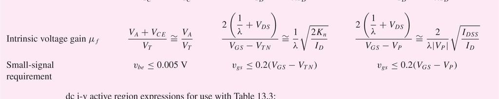
17 BJT Small-Signal Operation Current Gain & Intrinsic Voltage Gain Intrinsic voltage gain is defined by: β o = g m r π = β F 1 β 1 I F C β F i C Q point β o > β F for i C < I M, and β o < β F for i C > I M. However, for simplicity β F and β o will be assumed to be equal µ f = g m r o = I C V T For V CE << V A µ f V A V T V A +V CE I C 40V A = V A +V CE V T µ f represents the maximum voltage gain an individual BJT can provide and does not change with operating point. 01/10/12 Chap 13-17
18 Small-Signal Operation BJT Hybrid-Pi Model - Summary Transconductance: g m = I C V T 40I C Input resistance: The hybrid-pi small-signal model is the intrinsic representation of the BJT. Small-signal parameters are controlled by the Q-point and are independent of geometry of the BJT r π = β o V T I C Output resistance: r o = V A +V CE I C = β o g m V A I C or β o = g m r π 01/10/12 Chap 13-18
19 BJT Small-Signal Operation Equivalent Forms of Small-Signal Model Voltage-controlled current source g mv be can be transformed into current-controlled current source, v be = i b r π g m v be = g m i b r π = β o i b i c = β o i b + v ce r o β o i b Basic relationship i c = βi b is useful in both dc and ac analysis when the BJT is in the forward-active region. 01/10/12 Chap 13-19
20 BJT Small-Signal Operation Small-Signal Definition i C = I S exp v BE = I S exp V BE + v be i C = I C + i c = I S exp V BE exp v be = I C exp v be V T I C + i c = I C 1+ v be + 1 V T 2 v be V T V T v i c = I be C v be + 1 v be V T 2 V T 6 V T 3 v be V T For linearity, i c should be proportional to v be with v be << 2V T or v be V. i C I C 1+ v be v = I C + I be C The change in i c that corresponds to small-signal operation is: V T V T i c I C = v be V T 0.005V 0.025V = V T V T = I C + g m v be V T 01/12/12 Chap 13-20
21 BJT Small-Signal Operation Small-Signal Model for pnp Transistor For the pnp transistor Signal current injected into base causes decrease in total collector current which is equivalent to increase in signal current entering collector. So the small-signal models for the npn and pnp devices are identical! 01/12/12 Chap 13-21
22 Common-Emitter Amplifiers Small-Signal Analysis - ac Equivalent Circuit ac equivalent circuit is constructed by assuming that all capacitances have zero impedance at signal frequency and dc voltage sources are ac ground. Assume that Q-point is already known. 01/12/12 Chap 13-22
23 Common-Emitter Amplifiers Small-Signal Equivalent Circuit Input voltage is applied to the base terminal Output signal appears at collector terminal Emitter is common to both input and output signals Thus circuit is termed a Common-Emitter (C-E) Amplifier. The terminal gain of the C-E amplifier is the gain from the base terminal to the collector terminal A vt CE = v c v b = g m R L R L = r o R C R 3 01/12/12 Chap 13-23
24 Common-Emitter Amplifiers Input Resistance and Signal Source Gain (β o +1)R E Define R ib as the input resistance looking into the base of the transistor: R ib = v b i b = r π The input resistance presented to v i is: R in = R I + R B R ib = R I + R B r π The signal source voltage gain is: A v CE = v o v i = v o v b v b v i = A vt CE R B r π R I + R B r π 01/12/12 Chap 13-24
25 Common-Emitter Amplifiers Rule of Thumb Design Estimate A CE CE R v = A B r π CE vt A vt R I + R B r π A CE vt = g m R L R L = r o R C R 3 Typically: r o >> R C and R 3 >> R C A v CE g m R C = 40I C R C I C R C represents the voltage dropped across collector resistor R C A typical design point is I C R C = V CC 3 A v CE 40 V CC 3 =13.3V CC To help account for all the approximations and have a number that is easy to remember, our "rule-of-thumb" estimate for the voltage gain becomes A v CE 10V CC 01/13/12 Chap 13-25
26 Common-Emitter Amplifiers Voltage Gain Example Problem: Calculate voltage gain, input resistance and maximum input signal level for a common-emitter amplifier with a specified Q-point Given data: β F = 100, V A = 75 V, Q-point is (0.245 ma, 3.39 V) Assumptions: Transistor is in active region, β O = β F. Signals are low enough to be considered small signals. Room temperature. Analysis: g m = 40I C = mA r o = V A +V CE I C = ( ) = 9.80 ms r π = β o = 100 =10.2 kω g m 9.8mS 75V V 0.245mA = 320 kω R B = R 1 R 2 =160kΩ 300kΩ =104 kω R L = r o R C R L = 320kΩ 22kΩ 100kΩ =17.1 kω R B r π =104kΩ 10.2kΩ = 9.29 kω 7/20/10 Chap 13-26
27 Common-Emitter Amplifiers Voltage Gain Example (cont.) Analysis (cont): R A v = g m R B r π L R I + R B R in = R I + R B r π r π =10.3 kω = 9.8mS 17.1kΩ ( ) 9.29kΩ = kΩ+ 9.29kΩ R v be = v B r π i R I + R B r v be 0.005V v i 5mV 10.3kΩ = 5.54 mv π 9.29kΩ ( ) = 151 Check the rule-of-thumb estimate: A v CE ( ) = 120 (ballpark estimate) ( ) = V What is the maximum amplitude of the output signal: v o 5.54mV 151 1/13/12 Chap 13-27
28 Common-Emitter Amplifiers Voltage Gain Example (cont.) Simulation Results: The graph below presents the output voltage for an input voltage that is a 5-mV, 10-kHz sine wave. Note that although the sine wave at first looks good, the positive and negative peak amplitudes are different indicating the presence of distortion. The input is near our small-signal limit for linear operation. 1/13/12 Chap 13-28
29 Common-Emitter Amplifiers Dual Supply Operation - Example Analysis: To find the Q-point, the dc equivalent circuit is constructed I B +V BE +(β F +1)I B ( )= 5 I B =3.71 µa I C =65I B =241 µa Problem: Find voltage gain, input and output resistances for the circuit above Given data: β F = 65, V A = 50 V Assumptions: Active-region operation, V BE = 0.7 V, small signal operating conditions. I E =66I B =245 µa I C V CE ( )I E ( 5)=0 V CE =3.67 V 1/28/12 Chap 13-29
30 Common-Emitter Amplifiers Dual Supply Operation - Example (cont.) Next we construct the ac equivalent and simplify it kω R in = R B r π =6.31 kω R out = R C r o = 9.57 kω ( ) A v CE = v o v i = g m R out R 3 R in = 84.0 R I + R in Gain Estimate: A CE v 10( V CC +V EE ) = 100 1/28/12 Chap 13-30
31 Small-Signal Operation MOSFET Small-Signal Model g π = i g v gs vds =0 g r = i g v ds v ds =0 = i G v GS Q-point = i G v DS Q-point Using a two-port y-parameter network, i d g m = vgs vds=0 i D = vgs Q-point i g = g π v gs + g r v ds i d = g m v gs + g o v ds The port variables can represent either time-varying part of total voltages and currents or small changes in them away from Q-point values. g o = i d v ds v ds =0 I G = 0 = i D v DS Q-point I D = K n ( 2 V V GS TN ) 2 ( 1+ λv DS ) 1/17/12 Chap 13-31
32 Small-Signal Operation MOSFET Small-Signal Model (cont.) I G = 0 I D = K n ( 2 V V GS TN ) 2 ( 1+ λv DS ) g π = i G v GS Q-point g r = i G v DS Q-point = 0 = 0 i g = g π v gs + g r v ds i d = g m v gs + g o v ds g m = i D v GS Q-point g o = i D v DS Q-point = K n ( 2 V V GS TN )( 1+ λv DS ) = = λ K n ( 2 V GS V TN ) 2 = λi D = 1+ λv DS 2I D V GS V TN I D 1 λ +V DS 1/17/12 Chap 13-32
33 Small-Signal Operation MOSFET Small-Signal Model - Summary Transconductance: g m = 2I D = 2K n I D V GS V TN Since gate is insulated from channel by gate-oxide input resistance of transistor is infinite. Small-signal parameters are controlled by the Q-point. For the same operating point, MOSFET has lower transconductance and an output resistance that is similar to the BJT. Output resistance: r o = 1 g o = 1+λV DS λi D 1 λi D Amplification factor for λv DS <<1: µ f =g m r o = 1+λV DS λi D 1 λ 2K n I D 1/17/12 Chap 13-33
34 MOSFET Small-Signal Operation Small-Signal Definition Assume λv DS <<1. Then i D K n ( 2 v V GS TN ) 2 for v DS v GS V TN For v GS = V GS + v gs, i D = I D +i d = K n 2 2 ( ) + v gs ( v GS V TN ) 2 + 2v gs V GS V TN 2 ( ) + v gs i d = K n 2 2v gs V GS V TN For linearity, i d should be proportional to v gs and we require v 2 gs << 2v gs V GS V TN or v gs << 2( V GS V TN ) v gs 0.2( V GS V TN ) ( ) Since the MOSFET can be biased with (V GS - V TN ) equal to several volts, it can handle much larger values of v gs than corresponding the values of v be for the BJT. The change in drain current that corresponds to small-signal operation is: i d = g m 2 v gs I D I D V GS V TN ( ) 0.2 V GS V TN i d 0.4 I D 1/17/12 Chap 13-34
35 MOSFET Small-Signal Operation Body Effect in Four-terminal MOSFETs Drain current depends on threshold voltage which in turn depends on v SB. Back-gate transconductance is: g mb = i D = i D v BS v Q-point SB Q-point i D g mb = VTN V TN v SB Q-point = ( g m η)=g m η 0 < η < 3 is called the back-gate transconductance parameter. The bulk terminal is a reverse-biased diode. Hence, no conductance from the bulk terminal to other terminals. 01/18/12 Chap 13-35
36 MOSFET Small-Signal Operation Small-Signal Model for PMOS Transistor For a PMOS transistor v SG = V GG v gg i D = I D i d Positive signal voltage v gg reduces sourcegate voltage of the PMOS transistor causing decrease in total current exiting the drain, equivalent to an increase in the signal current entering the drain. The NMOS and PMOS small-signal models are the same! 01/18/12 Chap 13-36
37 Common-Source Amplifiers Small-Signal Analysis - ac Equivalent Circuit ac equivalent circuit is constructed by assuming that all capacitances have zero impedance at signal frequency and dc voltage sources are ac ground. 01/19/12 Chap 13-37
38 Common-Source Amplifiers Small-Signal Equivalent Circuit Input voltage is applied to the gate terminal Output signal appears at the drain terminal Source is common to both input and output signals Thus circuit is termed a Common-Source (C-S) Amplifier. The terminal gain of the C-S amplifier is the gain from the gate terminal to the drain terminal A vt CE = v d v g = g m R L R L = r o R D R 3 01/19/12 Chap 13-38
39 Common-Source Amplifiers Input Resistance and Signal-Source Gain Define R ig as the input resistance looking into the base of the transistor. R vg ig = = R G ii R in is the resistance presented to v i. R in = R I + R G The signal source voltage gain is: A v CS = v o v i = v o v g v g v i CS = A vt A CS R v = g m R G L R I + R G R G R I + R G 01/12/12 Chap 13-39
40 Common-Source Amplifiers Rule of Thumb Design Estimate R A CS v = g m R G L A vt R I + R G CS A CS vt = g m R L R L = r o R D R 3 I Typically: r o >> R D and R 3 >> R D A CS v g m R D = D R D V GS V TN 2 I D R D represents the voltage dropped across drain resistor R D A typical design point is I D R D = V DD 2 with V GS V TN =1 V A v CS V DD Our rule-of-thumb estimate for the C-S amplifier: the voltage gain equals the power supply voltage. Note that this is 10 times smaller than that for the BJT! 01/19/12 Chap 13-40
41 Common-Source Amplifiers Voltage Gain Example Problem: Calculate voltage gain, input resistance and maximum input signal level for a common-source amplifier with a specified Q-point Given data: Κ n = 0.50 ma/v 2, V TN = 1 V, λ = V -1, Q-point is (0.241 ma, 3.81 V) Assumptions: Transistor is in the active region. Signals are low enough to be considered small signals. Analysis: g m = 2K n I D ( 1+ λv DS ) = ms r o = λ 1 +V DS I D = 328 kω R G = R 1 R 2 = 892 kω R L = r o R D R 3 =17.1 kω 1/25/12 Chap 13-41
42 Common-Source Amplifiers Voltage Gain Example (cont.) g m = ms r o = 328 kω R G = 892 kω R L =17.1 kω R A CS v = g m R G 892kΩ L = 0.503mS ( 17.1kΩ) = R I + R G 1kΩ+892kΩ R R in = R I + R G = 893 kω v gs = v G R i v G i 0.2 V GS V TN R I + R G R I + R G V GS V TN 2I D K n = V v i V ( ) 893kΩ ( ) = 8.59 ( ) = V 892kΩ Check the rule-of-thumb estimate: A v CS V DD = 12 V (ballpark estimate) 1/25/12 Chap 13-42
43 Common-Source Amplifiers Voltage Gain Example (cont.) Simulation Results: The graph below presents the output voltage for an input voltage that is a 0.15-V, 10-kHz sine wave. The expected output voltage amplitude is vo = 8.59(0.15) = 1.29 V. Note that although the sine wave at first looks good, the positive and negative peak amplitudes are different indicating the presence of distortion, and the amplitude is actually larger than expected. The input is near our small-signal limit for linear operation. 1/25/12 Chap 13-43
44 C-E and C-S Amplifiers Output Resistance 01/19/12 Chap 13-44
45 C-E and C-S Amplifiers Output Resistance (cont.) Apply test source v x and find i x (with v i = 0) v be = 0 g m v be = 0 R out = v x i x = R C r o R out R C for r o >> R C v gs = 0 g m v gs = 0 R out = v x i x = R D r o R out R D for r o >> R D For comparable bias points, output resistances of C-S and C-E amplifiers are similar. 01/19/12 Chap 13-45
46 JFET Small-Signal Operation Small-Signal Model g g = 1 r g = i G v GS Q-point = I G + I SG V T 0 for I G = 0 i D = I DSS 1 v GS V P for v DS v GS V P i G = I SG exp v GS 1 V T 2 ( 1+ λv DS ) g m = i D = v GS Q-point g o = 1 r o = i D v DS Q-point 2I D 2 I DSS V 2 GS V P V GS V P V P = I D 1 λ +V DS ( ) 01/18/12 Microelectronic Circuit Design Chap 13-46
47 JFET Small-Signal Operation Small-Signal Model (cont.) For small-signal operation, the input signal limit is: v gs <0.2( V GS V P ) Since JFET is normally operated with gate junction reverse-biased, I G = I SG r g = The amplification factor is given by: 1 µ f = g m r o = 2 λ +V DS 2 V GS V λv P P I DSS I D 01/18/12 Microelectronic Circuit Design Chap 13-47
48 Common-Source Amplifiers JFET Example Analysis: Dc equivalent circuit is constructed. Ι G = 0, Ι S = Ι D. V GS = 2000I D V GS = ( )( )1 V GS ( 1) Choose V GS less negative than V P. 2 Problem: Find voltage gain, input and output resistances. Given data: Ι DSS = 1 ma, V P = -1V, λ = 0.02 V -1 Assumptions: Pinch-off region of operation. V GS = 0.5 V I D = ma 12= 27,000I D +V DS +2000I S V DS = 4.75V 1/28/12 Microelectronic Circuit Design Chap 13-48
49 Common-Source Amplifier JFET Example (cont.) Next we construct the ac equivalent and simplify it. 1/28/12 Microelectronic Circuit Design Chap 13-49


50 BJT and FET Small-Signal Model Summary 01/18/12 Chap 13-50

51 Common-Emitter/Common-Source Amplifiers Summary 1/25/11 Chap 13-51
52 Amplifier Power Dissipation Static power dissipation in amplifiers is found from their dc equivalent circuits. (a) Total power dissipated in the C-B and E-B junctions is: P D = V CE I C + V BE I B Total power supplied is: P S = V CC I C + V EE I E where V CE = V CB + V BE (b) Total power dissipated in the transistor is: P D = V DS I D + V GS I G = V DS I D Total power supplied is: P S = V DD I D +V DD2 /(R 1 +R 2 ) 1/28/12 Chap 13-52
53 Amplifier Signal Range v CE = V CE V m sinωt where V m is the output signal. Active region operation requires v CE v BE So: V m V CE V BE Also: v Rc ( t) = I C R C V m sinωt 0 ( ) V m min I C R C, V CE V BE Similarly for MOSFETs and JFETs: V M min I D R D,(V DS (V GS V TN )) V M min I D R D,(V DS (V GS V P )) 1/28/12 Chap 13-53
54 End of Chapter 13 1/28/12 Chap 13-54
Biasing the CE Amplifier
 Biasing the CE Amplifier Graphical approach: plot I C as a function of the DC base-emitter voltage (note: normally plot vs. base current, so we must return to Ebers-Moll): I C I S e V BE V th I S e V th
Circle the one best answer for each question. Five points per question.
 ID # NAME EE-255 EXAM 3 November 8, 2001 Instructor (circle one) Talavage Gray This exam consists of 16 multiple choice questions and one workout problem. Record all answers to the multiple choice questions
Electronic Circuits 1. Transistor Devices. Contents BJT and FET Characteristics Operations. Prof. C.K. Tse: Transistor devices
 Electronic Circuits 1 Transistor Devices Contents BJT and FET Characteristics Operations 1 What is a transistor? Three-terminal device whose voltage-current relationship is controlled by a third voltage
ID # NAME. EE-255 EXAM 3 April 7, Instructor (circle one) Ogborn Lundstrom
 Ogborn Lundstrom") ID # NAME EE-255 EXAM 3 April 7, 1998 Instructor (circle one) Ogborn Lundstrom This exam consists of 20 multiple choice questions. Record all answers on this page, but you must turn in the entire exam.
ID # NAME EE-255 EXAM 3 April 7, 1998 Instructor (circle one) Ogborn Lundstrom This exam consists of 20 multiple choice questions. Record all answers on this page, but you must turn in the entire exam.
Chapter 4 Field-Effect Transistors
 Chapter 4 Field-Effect Transistors Microelectronic Circuit Design Richard C. Jaeger Travis N. Blalock 5/5/11 Chap 4-1 Chapter Goals Describe operation of MOSFETs. Define FET characteristics in operation
EE105 Fall 2014 Microelectronic Devices and Circuits
 EE05 Fall 204 Microelectronic Devices and Circuits Prof. Ming C. Wu wu@eecs.berkeley.edu 5 Sutardja Dai Hall (SDH) Terminal Gain and I/O Resistances of BJT Amplifiers Emitter (CE) Collector (CC) Base (CB)
Bipolar Junction Transistor (BJT) - Introduction
 - Introduction") Bipolar Junction Transistor (BJT) - Introduction It was found in 1948 at the Bell Telephone Laboratories. It is a three terminal device and has three semiconductor regions. It can be used in signal amplification
Bipolar Junction Transistor (BJT) - Introduction It was found in 1948 at the Bell Telephone Laboratories. It is a three terminal device and has three semiconductor regions. It can be used in signal amplification
Homework Assignment 08
 Homework Assignment 08 Question 1 (Short Takes) Two points each unless otherwise indicated. 1. Give one phrase/sentence that describes the primary advantage of an active load. Answer: Large effective resistance
1. (50 points, BJT curves & equivalent) For the 2N3904 =(npn) and the 2N3906 =(pnp)
 For the 2N3904 =(npn) and the 2N3906 =(pnp)") HW 3 1. (50 points, BJT curves & equivalent) For the 2N3904 =(npn) and the 2N3906 =(pnp) a) Obtain in Spice the transistor curves given on the course web page except do in separate plots, one for the npn
HW 3 1. (50 points, BJT curves & equivalent) For the 2N3904 =(npn) and the 2N3906 =(pnp) a) Obtain in Spice the transistor curves given on the course web page except do in separate plots, one for the npn
6.012 Electronic Devices and Circuits Spring 2005
 6.012 Electronic Devices and Circuits Spring 2005 May 16, 2005 Final Exam (200 points) -OPEN BOOK- Problem NAME RECITATION TIME 1 2 3 4 5 Total General guidelines (please read carefully before starting):
ECE-342 Test 3: Nov 30, :00-8:00, Closed Book. Name : Solution
 ECE-342 Test 3: Nov 30, 2010 6:00-8:00, Closed Book Name : Solution All solutions must provide units as appropriate. Unless otherwise stated, assume T = 300 K. 1. (25 pts) Consider the amplifier shown
Vidyalankar S.E. Sem. III [EXTC] Analog Electronics - I Prelim Question Paper Solution
![Vidyalankar S.E. Sem. III [EXTC] Analog Electronics - I Prelim Question Paper Solution](/thumbs/90/101612294.jpg "Vidyalankar S.E. Sem. III [EXTC] Analog Electronics - I Prelim Question Paper Solution") . (a) S.E. Sem. [EXTC] Analog Electronics - Prelim Question Paper Solution Comparison between BJT and JFET BJT JFET ) BJT is a bipolar device, both majority JFET is an unipolar device, electron and minority
. (a) S.E. Sem. [EXTC] Analog Electronics - Prelim Question Paper Solution Comparison between BJT and JFET BJT JFET ) BJT is a bipolar device, both majority JFET is an unipolar device, electron and minority
ECE-343 Test 2: Mar 21, :00-8:00, Closed Book. Name : SOLUTION
 ECE-343 Test 2: Mar 21, 2012 6:00-8:00, Closed Book Name : SOLUTION 1. (25 pts) (a) Draw a circuit diagram for a differential amplifier designed under the following constraints: Use only BJTs. (You may
GEORGIA INSTITUTE OF TECHNOLOGY School of Electrical and Computer Engineering
 NAME: GEORGIA INSTITUTE OF TECHNOLOGY School of Electrical and Computer Engineering ECE 4430 First Exam Closed Book and Notes Fall 2002 September 27, 2002 General Instructions: 1. Write on one side of
Lecture 15: MOS Transistor models: Body effects, SPICE models. Context. In the last lecture, we discussed the modes of operation of a MOS FET:
 Lecture 15: MOS Transistor models: Body effects, SPICE models Context In the last lecture, we discussed the modes of operation of a MOS FET: oltage controlled resistor model I- curve (Square-Law Model)
EE 230 Lecture 31. THE MOS TRANSISTOR Model Simplifcations THE Bipolar Junction TRANSISTOR
 EE 23 Lecture 3 THE MOS TRANSISTOR Model Simplifcations THE Bipolar Junction TRANSISTOR Quiz 3 Determine I X. Assume W=u, L=2u, V T =V, uc OX = - 4 A/V 2, λ= And the number is? 3 8 5 2? 6 4 9 7 Quiz 3
EE 330 Lecture 22. Small Signal Modelling Operating Points for Amplifier Applications Amplification with Transistor Circuits
 EE 330 Lecture 22 Small Signal Modelling Operating Points for Amplifier Applications Amplification with Transistor Circuits Exam 2 Friday March 9 Exam 3 Friday April 13 Review Session for Exam 2: 6:00
EE 230 Lecture 33. Nonlinear Circuits and Nonlinear Devices. Diode BJT MOSFET
 EE 230 Lecture 33 Nonlinear Circuits and Nonlinear Devices Diode BJT MOSFET Review from Last Time: n-channel MOSFET Source Gate L Drain W L EFF Poly Gate oxide n-active p-sub depletion region (electrically
CHAPTER 3: TRANSISTOR MOSFET DR. PHAM NGUYEN THANH LOAN. Hà Nội, 9/24/2012
 1 CHAPTER 3: TRANSISTOR MOSFET DR. PHAM NGUYEN THANH LOAN Hà Nội, 9/24/2012 Chapter 3: MOSFET 2 Introduction Classifications JFET D-FET (Depletion MOS) MOSFET (Enhancement E-FET) DC biasing Small signal
Chapter 5. BJT AC Analysis
 Chapter 5. Outline: The r e transistor model CB, CE & CC AC analysis through r e model common-emitter fixed-bias voltage-divider bias emitter-bias & emitter-follower common-base configuration Transistor
CHAPTER.4: Transistor at low frequencies
 CHAPTER.4: Transistor at low frequencies Introduction Amplification in the AC domain BJT transistor modeling The re Transistor Model The Hybrid equivalent Model Introduction There are three models commonly
Capacitors Diodes Transistors. PC200 Lectures. Terry Sturtevant. Wilfrid Laurier University. June 4, 2009
 Wilfrid Laurier University June 4, 2009 Capacitor an electronic device which consists of two conductive plates separated by an insulator Capacitor an electronic device which consists of two conductive
Homework Assignment 09
 Homework Assignment 09 Question 1 (Short Takes) Two points each unless otherwise indicated. 1. What is the 3-dB bandwidth of the amplifier shown below if r π = 2.5K, r o = 100K, g m = 40 ms, and C L =
Lecture 24 Multistage Amplifiers (I) MULTISTAGE AMPLIFIER
 MULTISTAGE AMPLIFIER") Lecture 24 Multistage Amplifiers (I) MULTISTAGE AMPLIFIER Outline. Introduction 2. CMOS multi-stage voltage amplifier 3. BiCMOS multistage voltage amplifier 4. BiCMOS current buffer 5. Coupling amplifier
Lecture 24 Multistage Amplifiers (I) MULTISTAGE AMPLIFIER Outline. Introduction 2. CMOS multi-stage voltage amplifier 3. BiCMOS multistage voltage amplifier 4. BiCMOS current buffer 5. Coupling amplifier
5. EXPERIMENT 5. JFET NOISE MEASURE- MENTS
 5. EXPERIMENT 5. JFET NOISE MEASURE- MENTS 5.1 Object The objects of this experiment are to measure the spectral density of the noise current output of a JFET, to compare the measured spectral density
Chapter 6: Field-Effect Transistors
 Chapter 6: Field-Effect Transistors slamic University of Gaza Dr. Talal Skaik FETs vs. BJTs Similarities: Amplifiers Switching devices mpedance matching circuits Differences: FETs are voltage controlled
Lecture 11: J-FET and MOSFET
 ENE 311 Lecture 11: J-FET and MOSFET FETs vs. BJTs Similarities: Amplifiers Switching devices Impedance matching circuits Differences: FETs are voltage controlled devices. BJTs are current controlled devices.
CHAPTER 7 - CD COMPANION
 Chapter 7 - CD companion 1 CHAPTER 7 - CD COMPANION CD-7.2 Biasing of Single-Stage Amplifiers This companion section to the text contains detailed treatments of biasing circuits for both bipolar and field-effect
MOS Transistors. Prof. Krishna Saraswat. Department of Electrical Engineering Stanford University Stanford, CA
 MOS Transistors Prof. Krishna Saraswat Department of Electrical Engineering S Stanford, CA 94305 saraswat@stanford.edu 1 1930: Patent on the Field-Effect Transistor! Julius Lilienfeld filed a patent describing
ESE319 Introduction to Microelectronics. Output Stages
 Output Stages Power amplifier classification Class A amplifier circuits Class A Power conversion efficiency Class B amplifier circuits Class B Power conversion efficiency Class AB amplifier circuits Class
Lecture 13 MOSFET as an amplifier with an introduction to MOSFET small-signal model and small-signal schematics. Lena Peterson
 Lecture 13 MOSFET as an amplifier with an introduction to MOSFET small-signal model and small-signal schematics Lena Peterson 2015-10-13 Outline (1) Why is the CMOS inverter gain not infinite? Large-signal
(Refer Slide Time: 1:49)
") Analog Electronic Circuits Professor S. C. Dutta Roy Department of Electrical Engineering Indian Institute of Technology Delhi Lecture no 14 Module no 01 Midband analysis of FET Amplifiers (Refer Slide
Analog Electronic Circuits Professor S. C. Dutta Roy Department of Electrical Engineering Indian Institute of Technology Delhi Lecture no 14 Module no 01 Midband analysis of FET Amplifiers (Refer Slide
Electronic Circuits Summary
 Electronic Circuits Summary Andreas Biri, D-ITET 6.06.4 Constants (@300K) ε 0 = 8.854 0 F m m 0 = 9. 0 3 kg k =.38 0 3 J K = 8.67 0 5 ev/k kt q = 0.059 V, q kt = 38.6, kt = 5.9 mev V Small Signal Equivalent
Mod. Sim. Dyn. Sys. Amplifiers page 1
 AMPLIFIERS A circuit containing only capacitors, amplifiers (transistors) and resistors may resonate. A circuit containing only capacitors and resistors may not. Why does amplification permit resonance
EE105 Fall 2014 Microelectronic Devices and Circuits. NMOS Transistor Capacitances: Saturation Region
 EE105 Fall 014 Microelectronic Devices and Circuits Prof. Ming C. Wu wu@eecs.berkeley.edu 511 Sutardja Dai Hall (SDH) 1 NMOS Transistor Capacitances: Saturation Region Drain no longer connected to channel
Figure 1: MOSFET symbols.
 c Copyright 2008. W. Marshall Leach, Jr., Professor, Georgia Institute of Technology, School of Electrical and Computer Engineering. The MOSFET Device Symbols Whereas the JFET has a diode junction between
KOM2751 Analog Electronics :: Dr. Muharrem Mercimek :: YTU - Control and Automation Dept. 1 4 DC BIASING BJTS (CONT D II )
") KOM2751 Analog Electronics :: Dr. Muharrem Mercimek :: YTU - Control and Automation Dept. 1 4 DC BIASING BJTS (CONT D II ) Most of the content is from the textbook: Electronic devices and circuit theory,
KOM2751 Analog Electronics :: Dr. Muharrem Mercimek :: YTU - Control and Automation Dept. 1 4 DC BIASING BJTS (CONT D II ) Most of the content is from the textbook: Electronic devices and circuit theory,
MICROELECTRONIC CIRCUIT DESIGN Second Edition
 MICROELECTRONIC CIRCUIT DESIGN Second Edition Richard C. Jaeger and Travis N. Blalock Answers to Selected Problems Updated 10/23/06 Chapter 1 1.3 1.52 years, 5.06 years 1.5 2.00 years, 6.65 years 1.8 113
ECE 342 Electronic Circuits. 3. MOS Transistors
 ECE 342 Electronic Circuits 3. MOS Transistors Jose E. Schutt-Aine Electrical & Computer Engineering University of Illinois jschutt@emlab.uiuc.edu 1 NMOS Transistor Typically L = 0.1 to 3 m, W = 0.2 to
SOME USEFUL NETWORK THEOREMS
 APPENDIX D SOME USEFUL NETWORK THEOREMS Introduction In this appendix we review three network theorems that are useful in simplifying the analysis of electronic circuits: Thévenin s theorem Norton s theorem
Review of Band Energy Diagrams MIS & MOS Capacitor MOS TRANSISTORS MOSFET Capacitances MOSFET Static Model
 Content- MOS Devices and Switching Circuits Review of Band Energy Diagrams MIS & MOS Capacitor MOS TRANSISTORS MOSFET Capacitances MOSFET Static Model A Cantoni 2009-2013 Digital Switching 1 Content- MOS
BJT Biasing Cont. & Small Signal Model
 BJT Biasing Cont. & Small Signal Model Conservative Bias Design (1/3, 1/3, 1/3 Rule) Bias Design Example Small-Signal BJT Models Small-Signal Analysis 1 Emitter Feedback Bias Design R B R C V CC R 1 R
Bipolar junction transistors
 Bipolar junction transistors Find parameters of te BJT in CE configuration at BQ 40 µa and CBQ V. nput caracteristic B / µa 40 0 00 80 60 40 0 0 0, 0,5 0,3 0,35 0,4 BE / V Output caracteristics C / ma
Introduction and Background
 Analog CMOS Integrated Circuit Design Introduction and Background Dr. Jawdat Abu-Taha Department of Electrical and Computer Engineering Islamic University of Gaza jtaha@iugaza.edu.ps 1 Marking Assignments
DEPARTMENT OF ECE UNIT VII BIASING & STABILIZATION AMPLIFIER:
 UNIT VII IASING & STAILIZATION AMPLIFIE: - A circuit that increases the amplitude of given signal is an amplifier - Small ac signal applied to an amplifier is obtained as large a.c. signal of same frequency
EE105 - Fall 2005 Microelectronic Devices and Circuits
 EE105 - Fall 005 Microelectronic Devices and Circuits ecture 7 MOS Transistor Announcements Homework 3, due today Homework 4 due next week ab this week Reading: Chapter 4 1 ecture Material ast lecture
EECS 105: FALL 06 FINAL
 University of California College of Engineering Department of Electrical Engineering and Computer Sciences Jan M. Rabaey TuTh 2-3:30 Wednesday December 13, 12:30-3:30pm EECS 105: FALL 06 FINAL NAME Last
Mod. Sim. Dyn. Sys. Amplifiers page 1
 AMPLIFIERS A circuit containing only capacitors, amplifiers (transistors) and resistors may resonate. A circuit containing only capacitors and resistors may not. Why does amplification permit resonance
Practice 3: Semiconductors
 Practice 3: Semiconductors Digital Electronic Circuits Semester A 2012 VLSI Fabrication Process VLSI Very Large Scale Integration The ability to fabricate many devices on a single substrate within a given
Microelectronic Circuit Design 4th Edition Errata - Updated 4/4/14
 Chapter Text # Inside back cover: Triode region equation should not be squared! i D = K n v GS "V TN " v & DS % ( v DS $ 2 ' Page 49, first exercise, second answer: -1.35 x 10 6 cm/s Page 58, last exercise,
Electronic Devices and Circuits Lecture 18 - Single Transistor Amplifier Stages - Outline Announcements. Notes on Single Transistor Amplifiers
 6.012 Electronic Devices and Circuits Lecture 18 Single Transistor Amplifier Stages Outline Announcements Handouts Lecture Outline and Summary Notes on Single Transistor Amplifiers Exam 2 Wednesday night,
ECE 342 Electronic Circuits. Lecture 6 MOS Transistors
 ECE 342 Electronic Circuits Lecture 6 MOS Transistors Jose E. Schutt-Aine Electrical & Computer Engineering University of Illinois jesa@illinois.edu 1 NMOS Transistor Typically L = 0.1 to 3 m, W = 0.2
6.012 Electronic Devices and Circuits
 Page 1 of 10 YOUR NAME Department of Electrical Engineering and Computer Science Massachusetts Institute of Technology 6.012 Electronic Devices and Circuits Exam No. 2 Thursday, November 5, 2009 7:30 to
Final Examination EE 130 December 16, 1997 Time allotted: 180 minutes
 Final Examination EE 130 December 16, 1997 Time allotted: 180 minutes Problem 1: Semiconductor Fundamentals [30 points] A uniformly doped silicon sample of length 100µm and cross-sectional area 100µm 2
BJT Biasing Cont. & Small Signal Model
 BJT Biasing Cont. & Small Signal Model Conservative Bias Design Bias Design Example Small Signal BJT Models Small Signal Analysis 1 Emitter Feedback Bias Design Voltage bias circuit Single power supply
ECE 523/421 - Analog Electronics University of New Mexico Solutions Homework 3
 ECE 523/42 - Analog Electronics University of New Mexico Solutions Homework 3 Problem 7.90 Show that when ro is taken into account, the voltage gain of the source follower becomes G v v o v sig R L r o
Charge-Storage Elements: Base-Charging Capacitance C b
 Charge-Storage Elements: Base-Charging Capacitance C b * Minority electrons are stored in the base -- this charge q NB is a function of the base-emitter voltage * base is still neutral... majority carriers
Switching circuits: basics and switching speed
 ECE137B notes; copyright 2018 Switching circuits: basics and switching speed Mark Rodwell, University of California, Santa Barbara Amplifiers vs. switching circuits Some transistor circuit might have V
Lecture 18. Common Source Stage
 ecture 8 OUTINE Basic MOSFET amplifier MOSFET biasing MOSFET current sources Common source amplifier eading: Chap. 7. 7.7. EE05 Spring 008 ecture 8, Slide Prof. Wu, UC Berkeley Common Source Stage λ =
FET Small-Signal Analysis
 CHAPTER FET mall-ignal Analysis 9 9.1 INTROUCTION Field-effect transistor amplifiers provide an excellent voltage gain with the added feature of a high input impedance. They are also considered low-power
55:041 Electronic Circuits The University of Iowa Fall Final Exam
 Final Exam Name: Score Max: 135 Question 1 (1 point unless otherwise noted) a. What is the maximum theoretical efficiency for a class-b amplifier? Answer: 78% b. The abbreviation/term ESR is often encountered
55:041 Electronic Circuits The University of Iowa Fall Exam 2
 Exam 2 Name: Score /60 Question 1 One point unless indicated otherwise. 1. An engineer measures the (step response) rise time of an amplifier as t r = 0.35 μs. Estimate the 3 db bandwidth of the amplifier.
Forward-Active Terminal Currents
 Forward-Active Terminal Currents Collector current: (electron diffusion current density) x (emitter area) diff J n AE qd n n po A E V E V th ------------------------------ e W (why minus sign? is by def.
KOM2751 Analog Electronics :: Dr. Muharrem Mercimek :: YTU - Control and Automation Dept. 1 7 DC BIASING FETS (CONT D)
") KOM751 Analog Electronics :: Dr. Muharrem Mercimek :: YTU Control and Automation Dept. 1 7 DC BIASING FETS (CONT D) Most of the content is from the textbook: Electronic devices and circuit theory, Robert
KOM751 Analog Electronics :: Dr. Muharrem Mercimek :: YTU Control and Automation Dept. 1 7 DC BIASING FETS (CONT D) Most of the content is from the textbook: Electronic devices and circuit theory, Robert
ECE 546 Lecture 11 MOS Amplifiers
 ECE 546 Lecture MOS Amplifiers Spring 208 Jose E. Schutt-Aine Electrical & Computer Engineering University of Illinois jesa@illinois.edu ECE 546 Jose Schutt Aine Amplifiers Definitions Used to increase
ELECTRONICS IA 2017 SCHEME
 ELECTRONICS IA 2017 SCHEME CONTENTS 1 [ 5 marks ]...4 2...5 a. [ 2 marks ]...5 b. [ 2 marks ]...5 c. [ 5 marks ]...5 d. [ 2 marks ]...5 3...6 a. [ 3 marks ]...6 b. [ 3 marks ]...6 4 [ 7 marks ]...7 5...8
MOS Transistor Theory
 MOS Transistor Theory So far, we have viewed a MOS transistor as an ideal switch (digital operation) Reality: less than ideal EE 261 Krish Chakrabarty 1 Introduction So far, we have treated transistors
CARLETON UNIVERSITY. FINAL EXAMINATION December DURATION 3 HOURS No. of Students 130
 ALETON UNIVESITY FINAL EXAMINATION December 005 DUATION 3 HOUS No. of Students 130 Department Name & ourse Number: Electronics ELE 3509 ourse Instructor(s): Prof. John W. M. ogers and alvin Plett AUTHOIZED
Figure 1 Basic epitaxial planar structure of NPN. Figure 2 The 3 regions of NPN (left) and PNP (right) type of transistors
 and PNP (right) type of transistors") Figure 1 Basic epitaxial planar structure of NPN Figure 2 The 3 regions of NPN (left) and PNP (right) type of transistors Lecture Notes: 2304154 Physics and Electronics Lecture 6 (2 nd Half), Year: 2007
Figure 1 Basic epitaxial planar structure of NPN Figure 2 The 3 regions of NPN (left) and PNP (right) type of transistors Lecture Notes: 2304154 Physics and Electronics Lecture 6 (2 nd Half), Year: 2007
Lecture 12: MOSFET Devices
 Lecture 12: MOSFET Devices Gu-Yeon Wei Division of Engineering and Applied Sciences Harvard University guyeon@eecs.harvard.edu Wei 1 Overview Reading S&S: Chapter 5.1~5.4 Supplemental Reading Background
Assignment 3 ELEC 312/Winter 12 R.Raut, Ph.D.
 Page 1 of 3 ELEC 312: ELECTRONICS II : ASSIGNMENT-3 Department of Electrical and Computer Engineering Winter 2012 1. A common-emitter amplifier that can be represented by the following equivalent circuit,
Lecture 010 ECE4430 Review I (12/29/01) Page 010-1
 Page 010-1") Lecture 010 4430 Review I (12/29/01) Page 0101 LTUR 010 4430 RVIW I (RAIN: HLM hap. 1) Objective The objective of this presentation is: 1.) Identify the prerequisite material as taught in 4430 2.) Insure
Lecture 010 4430 Review I (12/29/01) Page 0101 LTUR 010 4430 RVIW I (RAIN: HLM hap. 1) Objective The objective of this presentation is: 1.) Identify the prerequisite material as taught in 4430 2.) Insure
Chapter 2 - DC Biasing - BJTs
 Objectives Chapter 2 - DC Biasing - BJTs To Understand: Concept of Operating point and stability Analyzing Various biasing circuits and their comparison with respect to stability BJT A Review Invented
ECE-305: Fall 2017 MOS Capacitors and Transistors
 ECE-305: Fall 2017 MOS Capacitors and Transistors Pierret, Semiconductor Device Fundamentals (SDF) Chapters 15+16 (pp. 525-530, 563-599) Professor Peter Bermel Electrical and Computer Engineering Purdue
DC Biasing. Dr. U. Sezen & Dr. D. Gökçen (Hacettepe Uni.) ELE230 Electronics I 15-Mar / 59
 ELE230 Electronics I 15-Mar / 59") Contents Three States of Operation BJT DC Analysis Fixed-Bias Circuit Emitter-Stabilized Bias Circuit Voltage Divider Bias Circuit DC Bias with Voltage Feedback Various Dierent Bias Circuits pnp Transistors
Contents Three States of Operation BJT DC Analysis Fixed-Bias Circuit Emitter-Stabilized Bias Circuit Voltage Divider Bias Circuit DC Bias with Voltage Feedback Various Dierent Bias Circuits pnp Transistors
ECE-343 Test 1: Feb 10, :00-8:00pm, Closed Book. Name : SOLUTION
 ECE-343 Test : Feb 0, 00 6:00-8:00pm, Closed Book Name : SOLUTION C Depl = C J0 + V R /V o ) m C Diff = τ F g m ω T = g m C µ + C π ω T = g m I / D C GD + C or V OV GS b = τ i τ i = R i C i ω H b Z = Z
ECE 546 Lecture 10 MOS Transistors
 ECE 546 Lecture 10 MOS Transistors Spring 2018 Jose E. Schutt-Aine Electrical & Computer Engineering University of Illinois jesa@illinois.edu NMOS Transistor NMOS Transistor N-Channel MOSFET Built on p-type
EE105 Fall 2015 Microelectronic Devices and Circuits Frequency Response. Prof. Ming C. Wu 511 Sutardja Dai Hall (SDH)
") EE05 Fall 205 Microelectronic Devices and Circuits Frequency Response Prof. Ming C. Wu wu@eecs.berkeley.edu 5 Sutardja Dai Hall (SDH) Amplifier Frequency Response: Lower and Upper Cutoff Frequency Midband
EE05 Fall 205 Microelectronic Devices and Circuits Frequency Response Prof. Ming C. Wu wu@eecs.berkeley.edu 5 Sutardja Dai Hall (SDH) Amplifier Frequency Response: Lower and Upper Cutoff Frequency Midband
Chapter7. FET Biasing
 Chapter7. J configurations Fixed biasing Self biasing & Common Gate Voltage divider MOS configurations Depletion-type Enhancement-type JFET: Fixed Biasing Example 7.1: As shown in the figure, it is the
Lecture 050 Followers (1/11/04) Page ECE Analog Integrated Circuits and Systems II P.E. Allen
 Page ECE Analog Integrated Circuits and Systems II P.E. Allen") Lecture 5 Followers (1/11/4) Page 51 LECTURE 5 FOLLOWERS (READING: GHLM 344362, AH 221226) Objective The objective of this presentation is: Show how to design stages that 1.) Provide sufficient output
Lecture 5 Followers (1/11/4) Page 51 LECTURE 5 FOLLOWERS (READING: GHLM 344362, AH 221226) Objective The objective of this presentation is: Show how to design stages that 1.) Provide sufficient output
Lecture 23: Negative Resistance Osc, Differential Osc, and VCOs
 EECS 142 Lecture 23: Negative Resistance Osc, Differential Osc, and VCOs Prof. Ali M. Niknejad University of California, Berkeley Copyright c 2005 by Ali M. Niknejad A. M. Niknejad University of California,
figure shows a pnp transistor biased to operate in the active mode
 Lecture 10b EE-215 Electronic Devices and Circuits Asst Prof Muhammad Anis Chaudhary BJT: Device Structure and Physical Operation The pnp Transistor figure shows a pnp transistor biased to operate in the
MOS Transistor I-V Characteristics and Parasitics
 ECEN454 Digital Integrated Circuit Design MOS Transistor I-V Characteristics and Parasitics ECEN 454 Facts about Transistors So far, we have treated transistors as ideal switches An ON transistor passes
At point G V = = = = = = RB B B. IN RB f
 Common Emitter At point G CE RC 0. 4 12 0. 4 116. I C RC 116. R 1k C 116. ma I IC 116. ma β 100 F 116µ A I R ( 116µ A)( 20kΩ) 2. 3 R + 2. 3 + 0. 7 30. IN R f Gain in Constant Current Region I I I C F
EE105 - Fall 2006 Microelectronic Devices and Circuits
 EE105 - Fall 2006 Microelectronic Devices and Circuits Prof. Jan M. Rabaey (jan@eecs) Lecture 7: MOS Transistor Some Administrative Issues Lab 2 this week Hw 2 due on We Hw 3 will be posted same day MIDTERM
UNIVERSITY OF CALIFORNIA, BERKELEY College of Engineering Department of Electrical Engineering and Computer Sciences
 UNIVERSITY OF CALIFORNIA, BERKELEY College of Engineering Department of Electrical Engineering and Computer Sciences EE 105: Microelectronic Devices and Circuits Spring 2008 MIDTERM EXAMINATION #1 Time
Fig. 1 CMOS Transistor Circuits (a) Inverter Out = NOT In, (b) NOR-gate C = NOT (A or B)
 Inverter Out = NOT In, (b) NOR-gate C = NOT (A or B)") 1 Introduction to Transistor-Level Logic Circuits 1 By Prawat Nagvajara At the transistor level of logic circuits, transistors operate as switches with the logic variables controlling the open or closed
1 Introduction to Transistor-Level Logic Circuits 1 By Prawat Nagvajara At the transistor level of logic circuits, transistors operate as switches with the logic variables controlling the open or closed
ESE 570: Digital Integrated Circuits and VLSI Fundamentals
 ESE 570: Digital Integrated Circuits and VLSI Fundamentals Lec 5: January 25, 2018 MOS Operating Regions, pt. 1 Lecture Outline! 3 Regions of operation for MOSFET " Subthreshold " Linear " Saturation!
Microelectronic Devices and Circuits Lecture 13 - Linear Equivalent Circuits - Outline Announcements Exam Two -
 6.012 Microelectronic Devices and Circuits Lecture 13 Linear Equivalent Circuits Outline Announcements Exam Two Coming next week, Nov. 5, 7:309:30 p.m. Review Subthreshold operation of MOSFETs Review Large
6.012 MICROELECTRONIC DEVICES AND CIRCUITS
 MASSACHUSETTS INSTITUTE OF TECHNOLOGY Department of Electrical Engineering and Computer Science 6.012 MICROELECTRONIC DEVICES AND CIRCUITS Answers to Exam 2 Spring 2008 Problem 1: Graded by Prof. Fonstad
EE 321 Analog Electronics, Fall 2013 Homework #8 solution
 EE 321 Analog Electronics, Fall 2013 Homework #8 solution 5.110. The following table summarizes some of the basic attributes of a number of BJTs of different types, operating as amplifiers under various
EE105 - Fall 2006 Microelectronic Devices and Circuits. Some Administrative Issues
 EE105 - Fall 006 Microelectronic evices and Circuits Prof. Jan M. Rabaey (jan@eecs Lecture 8: MOS Small Signal Model Some Administrative Issues REIEW Session Next Week Tu Sept 6 6:00-7:30pm; 060 alley
Circuits. L2: MOS Models-2 (1 st Aug. 2013) B. Mazhari Dept. of EE, IIT Kanpur. B. Mazhari, IITK. G-Number
 B. Mazhari Dept. of EE, IIT Kanpur. B. Mazhari, IITK. G-Number") EE610: CMOS Analog Circuits L: MOS Models- (1 st Aug. 013) B. Mazhari Dept. of EE, IIT Kanpur 3 NMOS Models MOS MODEL Above Threshold Subthreshold ( GS > TN ) ( GS < TN ) Saturation ti Ti Triode ( DS >
EE610: CMOS Analog Circuits L: MOS Models- (1 st Aug. 013) B. Mazhari Dept. of EE, IIT Kanpur 3 NMOS Models MOS MODEL Above Threshold Subthreshold ( GS > TN ) ( GS < TN ) Saturation ti Ti Triode ( DS >
ESE319 Introduction to Microelectronics. BJT Biasing Cont.
 BJT Biasing Cont. Biasing for DC Operating Point Stability BJT Bias Using Emitter Negative Feedback Single Supply BJT Bias Scheme Constant Current BJT Bias Scheme Rule of Thumb BJT Bias Design 1 Simple
ECE 205: Intro Elec & Electr Circuits
 ECE 205: Intro Elec & Electr Circuits Final Exam Study Guide Version 1.00 Created by Charles Feng http://www.fenguin.net ECE 205: Intro Elec & Electr Circuits Final Exam Study Guide 1 Contents 1 Introductory
ECE315 / ECE515 Lecture-2 Date:
 Lecture-2 Date: 04.08.2016 NMOS I/V Characteristics Discussion on I/V Characteristics MOSFET Second Order Effect NMOS I-V Characteristics ECE315 / ECE515 Gradual Channel Approximation: Cut-off Linear/Triode
6.012 Electronic Devices and Circuits
 Page 1 of 12 YOUR NAME Department of Electrical Engineering and Computer Science Massachusetts Institute of Technology 6.012 Electronic Devices and Circuits FINAL EXAMINATION Open book. Notes: 1. Unless
Device Physics: The Bipolar Transistor
 Monolithic Amplifier Circuits: Device Physics: The Bipolar Transistor Chapter 4 Jón Tómas Guðmundsson tumi@hi.is 2. Week Fall 2010 1 Introduction In analog design the transistors are not simply switches
Chapter 2 CMOS Transistor Theory. Jin-Fu Li Department of Electrical Engineering National Central University Jungli, Taiwan
 Chapter 2 CMOS Transistor Theory Jin-Fu Li Department of Electrical Engineering National Central University Jungli, Taiwan Outline Introduction MOS Device Design Equation Pass Transistor Jin-Fu Li, EE,
The Devices. Digital Integrated Circuits A Design Perspective. Jan M. Rabaey Anantha Chandrakasan Borivoje Nikolic. July 30, 2002
 Digital Integrated Circuits A Design Perspective Jan M. Rabaey Anantha Chandrakasan Borivoje Nikolic The Devices July 30, 2002 Goal of this chapter Present intuitive understanding of device operation Introduction