FIELD-EFFECT TRANSISTORS
|
|
|
- Philippa Bates
- 6 years ago
- Views:
Transcription
1 FIEL-EFFECT TRANSISTORS 1 Semiconductor review 2 The MOS capacitor 2 The enhancement-type N-MOS transistor 3 I-V characteristics of enhancement MOSFETS 4 The output characteristic of the MOSFET in saturation 5 The PMOS transistor 6 Real MOSFET characteristics 7 CMOS design rules 1
2 Semiconductors Four types of charge are present inside a semiconductor: the fixed positive charge of ionized donors, the fixed negative charge of ionized acceptors, the positive mobile charge of holes, and the negative mobile charge of electrons. We consider all donors and acceptors ionized N = N and N = N + A A On this basis, the net positive charge density ρ is ρ = q( N N + p n) A 2
3 Boltzmann s Law (1) In equilibrium electrons and holes follow Boltzmann s law and their concentrations (number per unit volume) are proportional to k=1.38x10⁻²³ J/K - Boltzmann constant T - absolute temperature (K). electron and hole densities in equilibrium are related to electrostatic potential φ by n( φ1) n( φ ) q=1.6x10⁻¹⁹ C 2 = e q( φ φ ) 1 2 kt -( Energy / kt ) e p( φ1) p( φ ) q( φ φ ) 3 2 = e 1 2 kt
4 n 0 and p 0 - equilibrium electron and hole concentrations in the neutral bulk (φ=0 ) u Boltzmann s Law (2) qφ qφ kt u kt = 0 = = 0 0 = 0 p p e p e = φ φ / t φ = kt / q t - normalized electrostatic potential - thermal voltage the mass-action law is n i - concentration of electrons (and holes) in the intrinsic semiconductor n n e n e 2 np = n i 4 u
5 Example: Calculate the built-in potential for a Si p-n junction with N A = atoms/cm 3 and N = atoms/cm 3,T=300K In equilibrium, if we choose the potential origin φ = 0 where the semiconductor is intrinsic (i.e., where p 0 =n 0 =n i ), then p 0 = / t nie φ φ Far from the junction in the n-side 0 n 0 = / t nie φ φ n region t n N n e φ = φ i / Far from the junction in the p-side The built-in potential is given by p region t p N n e φ = φ 0 A i / N N A NN A φbi = φn region φp region = φt ln φt ln = φt ln 2 n i n i ni 15 ( ) φ 26 ln mv bi 5
6 The two-terminal MOS structure 6
7 The ideal two-terminal MOS structure (V FB =0) V G C ox = Aε t ox ox V Q G G φ = s Q C + Q = C G ox + φ s _ 0 Q G Q C M O S A - capacitor area, t ox - oxide thickness ε ox - permittivity of oxide Q C ε Q G = ; C ox = = A A t V G G ox ox φ Q C = s Cox ox 7
8 Example: oxide capacitance (a) Calculate the oxide capacitance per unit area for t ox = 5 and 20 nm assuming ε ox = 3.9ε 0, where ε 0 = F/cm is the permittivity of free space. (b) etermine the area of a 1pF metal-oxide-metal capacitor for the two oxide thicknesses given in (a). Answer: (a) =690 nf/cm 2 = 6.9 ff/µm 2 for t ox =5 nm and = 172 nf/cm 2 = 1.7 ff/µm 2 for t ox = 20 nm. The capacitor areas are 145 and 580 µm 2 for oxide thicknesses of 5 and 20 nm, respectively. 8
9 The flat-band voltage In equilibrium (with the two terminals shortened/open), the contact potential between the gate and the semiconductor substrate of the MOS induces charges in the gate and the semiconductor for V GB =0. Charges inside the insulator and at the semiconductor-insulator interface also induce a semiconductor charge at zero bias. The effect of the contact potential and oxide charges can be counterbalanced by applying a gate-bulk voltage called the flat-band voltage V FB. V Q V = φ C G FB s C ox 9
10 Example: flat-band voltage (a) etermine the expression for the flat-band voltage of n + polysilicon-gate on p-type silicon (b) Calculate the flat-band voltage for an n + polysilicon-gate on p-type silicon structure with N A = atoms/cm 3. Answer: (a) In equilibrium, by analogy with an n + p junction, the potential of the n + -region is positive with respect to that of the p- region. The flat-band condition is obtained by applying a negative potential to the n + gate with respect to the p-type semiconductor of value (b) V V N A _ + = φ _ + = 0.56 V φ ln ni 7 = 0.56 V φ ln 10 = 980 mv FB n p bi n p t FB t ( ) 10
11 Regions of operation of the MOSFET: Accumulation (p-substrate) V GB Q G G Q o Q C V Q φ G B s < V > 0 C < 0 F B Holes + accumulate in the p-type semiconductor surface B 11
12 Regions of operation of the MOSFET: epletion (p-substrate) Q G G V Q 0 > V < 0 G B C < φ < s F B φ F V GB Q o Q - - C Holes evacuate from the P semiconductor surface and acceptor ion charges become uncovered - B φ F = Fermi potential ( to be defined) 12
13 Regions of operation of the MOSFET: Inversion (p-substrate) V GB Q G G Q o Q C V Q φ G B s < C > > φ V 0 F F B electrons approach the surface! B 13
14 Inversion for p-type substrate Volume charge density inside the semiconductor: ρ = q( p e n e + n p ) u u epletion of holes prevails over electron charge when p e > n e u 0 0 u or, equivalently φ < φ t 2 p 0 ln( ) n 0 mass-action law φt p p = ln( ) = ln( ) = φf 2 n φ 2 t i ni For φ >φ F the concentration of minority carriers (n) becomes higher than that of majority carriers (p); the semiconductor operates in the inversion region 14
15 Strong Inversion for p-type substrate Volume charge density inside the semiconductor: ρ = q( p e n e + n p ) u u Electron (minority carrier) density equals the hole ( majority carrier) deep in the bulk n e > p u 0 0 φ > φ p 0 t ln( ) n0 mass-action law φ p φ p = = = φ t ln( ) 2 ln( ) 2 2 t F ni ni For φ >2φ F the concentration of minority carriers (n) becomes higher than that of majority carriers (p) deep in the bulk; the semiconductor operates in the strong inversion region 15
16 Threshold voltage ( for strong inversion) Gate voltage for which φ s = 2φ At threshold we can neglect the inversion charge Q I compared with the depletion charge Q B F Recalling that V Q Q V = φ φ C C G FB s s Cox B ox Q qn x = 2 qε N φ B A d s A s it follows that V V + 2φ + γ 2 φ T FB F F γ = 2 qε N / C s A ox 16
17 Example: threshold voltage Estimate V T for an n-channel transistor with n + polysilicon gate, N A =10 17 atoms/cm 3 and t ox =5 nm. Answer: The flat-band voltage (slide 10) is V; φ F =0.419; C ox = 690 nf/cm 2. The body-effect factor is γ = 2 qε N / C = V s A ox V V + 2φ + γ 2 φ = = 0.1V T FB F F For this low value of the threshold voltage, the off-current (for V GS =0) is too high for digital circuits. Solution to control the magnitude of the threshold voltage without an exaggerated increase in the slope factor a non-uniform high-low channel doping. 17
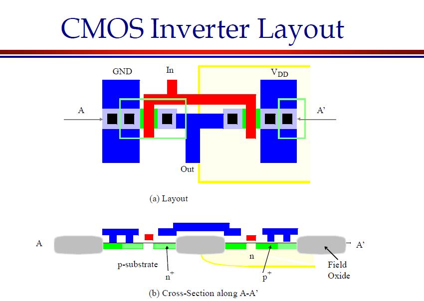
18 5.3 The Enhancement-Type NMOS Transistor n + Source Region W S Channel Region B L G n n+ + rain Region Metal Silicon ioxide ( SiO ) 2 P-Type Substrate (Body) 0.8 µ CMOS technology L min = 0.8 µm metal width 1.4 µm Wmin = 2.0 µm t ox = 160 Å X j = 0.40 µm Source (S) v S i i G i S Gate (G) n + Channel Region n + L v G P-Type Substrate Body (B) v rain () x j ( a ) NMOS transistor structure ( b ) cross section and ( c ) circuit symbol 18 G i i G i B i S S B i B v B i G = 0 i B = 0 i = i S
 V GS <V")
19 MOSFET in subthreshold (weak inversion) V GS <V T 19
20 MOSFET for V GS >V T in the linear region 20

21 MOSFET for V GS >V T in the triode region 21

22 MOSFET for V GS >V T in the saturation region 22
23 (a) n + S Immobile Acceptor Ion p V << V GS TN n + epletion Region ( a ) No ( electron ) channel between source and drain. B (b) (c) S S p p V < V GS TN n + n + V > V GS TN n + n + B n-type Inversion Layer B epletion Region epletion Region ( b ) No ( electron ) channel between source and drain. In fact, a weakly inverted layer can be induced in the substrate ( weak inversion ). ( c ) The electric field induces an electron channel that connects the source and drain islands. ( a ) V GS << V TN ( b ) V GS < V TN ( c ) V GS > V TN 23
24 V S V G 2V N + N + V V S V G V 1V 2V 1V N + N + P B P B V G = 2V V S = V = 0V ions ( a ) electrons V G = 2V V S = V = 1V ( b ) V G N + N + P B 1V ( a ) MOSFET in the linear region for V = V S = 0V ( b ) MOSFET in the linear region for V = V S = 1V ( c ) MOSFET in the linear region for V = 1V, V S = 0V V G = 2V V S = 0V V = 1V ( c ) 24
 MOSFET in the linear region ( b ) MOSFET with channel just pinched off at the drain.")
25 S n + G v > V GS TN n + v Small S Waterfalls analogy Water epletion Region p Acceptor Ion B S G v > V GS TN v = v - V S GS TN n + n + epletion Region p B S G v > V GS TN v > v - V S GS TN epletion Region n + p n + Pinch-off Point B ( a ) MOSFET in the linear region ( b ) MOSFET with channel just pinched off at the drain. ( c ) Channel pinch off for V S > V GS - V TN 25
26 MOSFET model: drift current y A z V X dx For low electric fields: v x = µ 7 vx vsat 10 cm/s n ε For high electric fields: ε x ε dq q n A dx Ix = = = q n A v x dt dt or J = q n x v x :electric field µ n : electron mobility µ n = µ n ( doping, T, electric field ) q: electronic charge =1.6 x10⁻¹⁹ C 26
27 rift current density J = J n + J p = ( q n µ n + q p µ p ) ε electron current hole current σ At T = 300 K and doping concentrations cm -3 µ n (Si) 1400 cm 2 /Vs, µ p (Si) 500 cm 2 /Vs µ depends on doping level, temperature and electric field. 27
28 5.4 I-V Characteristics of the Enhancement MOSFET Simplified Analysis z x y V S Substrate is grounded φ V G SiO2 Channel length: L Channel width: W I V Q gate = - Q semi -Q I ( Q depletion is negligible ) Q I - C OX ( V G V T0 - φ ) ( inversion layer is very thin ) Q I : inversion charge/area (inversion charge density) ε OX C OX = : oxide capacitance / area TOX 28
29 Strong inversion (linear ) charge model 29
30 For small V S : I K n ( V GS V T ) V S = K ( V V ) 8.00e-4 and di dv V = 5 V GS S n GS T rain-source Current (A) 6.00e e e-4 V GS = 4 V V GS = 3 V V = 2 V GS 0.00e rain-source Voltage (V) 0.8 NMOS i-v characteristics in the linear region (VSB = 0) 30
31 rain-source Current (A) 2.20e e e e e e e e e e e e+0 0 Linear Region 2 V = 5 V GS Pinchoff Locus Saturation Region V GS= 4 V V = 3 V GS V Š 1 V V = 2 V GS GS rain-source Voltage (V) 12 I I 0 for V GS V T W S ( ) V + V I = µ C V V V L 2 n OX G T S = V GS V T V S V SSAT K 2 n ( V V ) 2 GS V GS V T V S V SSAT T Output characteristics for an NMOS transistor with V TN = 1 V and K n = 25 x 10-6 A / V 2 I G B V V S 31 S
32 The PMOS Transistor Source v v < 0 S G v < 0 i i S G Gate i rain p + Channel Region p + L N-Type Substrate Body i B v > 0 B Cross section of an enhancement-mode PMOS transistor S S B I I G G 32
33 Source-rain Current (A) 2.50e e e e e e+0 V = 5 V (V = -5 V) SG GS V = 4 V (V = -4 V) SG GS V = 3 V (V = -3 V) SG GS V = 2 V (V = -2 V) SG GS V Š 1 V (V -1 V) SG GS I 0 for V GS V T S ( ) V + V I = K V V V 2 P G T S I = V GS V T V S V SSAT K 2 p ( V V ) 2 GS T -5.00e Source-rain Voltage (V) V GS V T V S V SSAT Output characteristics for a PMOS transistor with V TP = -1 V and K P = 25 x 10-6 A / V 2 G S B 33 I
34 The CMOS Technology V (0 V) SS v I V (5 V) B S v o S B p+ Ohmic contact n+ n+ p+ p+ n-well NMOS transistor PMOS transistor p-type substrate n+ Ohmic contact N-well CMOS structure for forming both NMOS & PMOS transistors in a single silicon substrate 34
35 Summary of C equations for the enhancement-mode MOSFET G S n-channel I B G G or V T > 0 V S 0 S K = µc S p-channel B G V T < 0 V S 0 ( a ) v GS < V T Cutoff region, i 0 v GS V T OX W L or S I ( b ) v GS V T Triode region v GS V T S ( v V ) v v V i = K ( vg VT ) vs v v V ( v V ) G T S GS T v + v 2 S GS T G T ( b ) v GS V T Saturation region v GS V T K 2 ( vg V T ) vs vgs VT i ( ) 2 = vgs VT v v V ( v V ) S GS T G T i ( b ) ( c ) V GS2 V GS2 ( c ) ( b ) i V GS1 V GS1 V ( a ) V S S ( a ) 35
36 I (A) E-03 Common-source characteristic of an channel MOSFET I ,00E-02 ( A ) 1.00E E-05 V B = V GB ,50E-02 V SB = V E ,00E-02 V B = V GB E E E-09 V SB = V V GB (V) ,00E ,00E V GB (V) V GB V SB 36

37 Subthreshold (weak inversion) model V GS <V T VG VT 0 VS / t n φ VS / φt 0 1 I = I e e C 2qε sn b A n=1+ = 1+ C 2 C 2 φ ox ox F 37 n:
38 38
39 39
40 40
41 41
42 42
43 43
44 44
45 45
46 46
47 References EEL 7061 Eletrônica Básica Reid R. Harrison, Analog Integrated Circuit esign ECE/CS 5720/6720 epartment of Electrical and Computer Engineering University of Utah. Márcio Cherem Schneider and Carlos Galup-Montoro, CMOS Analog esign Using All-Region MOSFET Modeling, Cambridge University Press, J. M. Rabaey, igital integrated Circuits, Prentice Hall,
CHAPTER 5 MOS FIELD-EFFECT TRANSISTORS
 CHAPTER 5 MOS FIELD-EFFECT TRANSISTORS 5.1 The MOS capacitor 5.2 The enhancement-type N-MOS transistor 5.3 I-V characteristics of enhancement mode MOSFETS 5.4 The PMOS transistor and CMOS technology 5.5
Integrated Circuits & Systems
 Federal University of Santa Catarina Center for Technology Computer Science & Electronics Engineering Integrated Circuits & Systems INE 5442 Lecture 10 MOSFET part 1 guntzel@inf.ufsc.br ual-well Trench-Isolated
The Devices. Digital Integrated Circuits A Design Perspective. Jan M. Rabaey Anantha Chandrakasan Borivoje Nikolic. July 30, 2002
 igital Integrated Circuits A esign Perspective Jan M. Rabaey Anantha Chandrakasan Borivoje Nikolic The evices July 30, 2002 Goal of this chapter Present intuitive understanding of device operation Introduction
Fundamentals of the Metal Oxide Semiconductor Field-Effect Transistor
 Triode Working FET Fundamentals of the Metal Oxide Semiconductor Field-Effect Transistor The characteristics of energy bands as a function of applied voltage. Surface inversion. The expression for the
EE 560 MOS TRANSISTOR THEORY
 1 EE 560 MOS TRANSISTOR THEORY PART 1 TWO TERMINAL MOS STRUCTURE V G (GATE VOLTAGE) 2 GATE OXIDE SiO 2 SUBSTRATE p-type doped Si (N A = 10 15 to 10 16 cm -3 ) t ox V B (SUBSTRATE VOLTAGE) EQUILIBRIUM:
ESE 570: Digital Integrated Circuits and VLSI Fundamentals
 ESE 570: Digital Integrated Circuits and VLSI Fundamentals Lec 4: January 23, 2018 MOS Transistor Theory, MOS Model Penn ESE 570 Spring 2018 Khanna Lecture Outline! CMOS Process Enhancements! Semiconductor
Lecture 12: MOS Capacitors, transistors. Context
 Lecture 12: MOS Capacitors, transistors Context In the last lecture, we discussed PN diodes, and the depletion layer into semiconductor surfaces. Small signal models In this lecture, we will apply those
ESE 570: Digital Integrated Circuits and VLSI Fundamentals
 ESE 570: Digital Integrated Circuits and VLSI Fundamentals Lec 4: January 24, 2017 MOS Transistor Theory, MOS Model Penn ESE 570 Spring 2017 Khanna Lecture Outline! Semiconductor Physics " Band gaps "
MOS Transistor I-V Characteristics and Parasitics
 ECEN454 Digital Integrated Circuit Design MOS Transistor I-V Characteristics and Parasitics ECEN 454 Facts about Transistors So far, we have treated transistors as ideal switches An ON transistor passes
The Devices: MOS Transistors
 The Devices: MOS Transistors References: Semiconductor Device Fundamentals, R. F. Pierret, Addison-Wesley Digital Integrated Circuits: A Design Perspective, J. Rabaey et.al. Prentice Hall NMOS Transistor
ESE 570: Digital Integrated Circuits and VLSI Fundamentals
 ESE 570: Digital Integrated Circuits and VLSI Fundamentals Lec 4: January 29, 2019 MOS Transistor Theory, MOS Model Penn ESE 570 Spring 2019 Khanna Lecture Outline! CMOS Process Enhancements! Semiconductor
Lecture 15 OUTLINE. MOSFET structure & operation (qualitative) Review of electrostatics The (N)MOS capacitor
 Review of electrostatics The (N)MOS capacitor") Lecture 15 OUTLINE MOSFET structure & operation (qualitative) Review of electrostatics The (N)MOS capacitor Electrostatics Charge vs. voltage characteristic Reading: Chapter 6.1 6.2.1 EE15 Spring 28 Lecture
Lecture 15 OUTLINE MOSFET structure & operation (qualitative) Review of electrostatics The (N)MOS capacitor Electrostatics Charge vs. voltage characteristic Reading: Chapter 6.1 6.2.1 EE15 Spring 28 Lecture
MOSFET: Introduction
 E&CE 437 Integrated VLSI Systems MOS Transistor 1 of 30 MOSFET: Introduction Metal oxide semiconductor field effect transistor (MOSFET) or MOS is widely used for implementing digital designs Its major
Lecture 04 Review of MOSFET
 ECE 541/ME 541 Microelectronic Fabrication Techniques Lecture 04 Review of MOSFET Zheng Yang (ERF 3017, email: yangzhen@uic.edu) What is a Transistor? A Switch! An MOS Transistor V GS V T V GS S Ron D
Charge Storage in the MOS Structure. The Inverted MOS Capacitor (V GB > V Tn )
") The Inverted MO Capacitor (V > V Tn ) We consider the surface potential as Þxed (ÒpinnedÓ) at φ s,max = - φ p φ(x).5 V. V V ox Charge torage in the MO tructure Three regions of operation: Accumulation:
The Inverted MO Capacitor (V > V Tn ) We consider the surface potential as Þxed (ÒpinnedÓ) at φ s,max = - φ p φ(x).5 V. V V ox Charge torage in the MO tructure Three regions of operation: Accumulation:
an introduction to Semiconductor Devices
 an introduction to Semiconductor Devices Donald A. Neamen Chapter 6 Fundamentals of the Metal-Oxide-Semiconductor Field-Effect Transistor Introduction: Chapter 6 1. MOSFET Structure 2. MOS Capacitor -
Lecture 6 PN Junction and MOS Electrostatics(III) Metal-Oxide-Semiconductor Structure
 Metal-Oxide-Semiconductor Structure") Lecture 6 PN Junction and MOS Electrostatics(III) Metal-Oxide-Semiconductor Structure Outline 1. Introduction to MOS structure 2. Electrostatics of MOS in thermal equilibrium 3. Electrostatics of MOS with
Lecture 6 PN Junction and MOS Electrostatics(III) Metal-Oxide-Semiconductor Structure Outline 1. Introduction to MOS structure 2. Electrostatics of MOS in thermal equilibrium 3. Electrostatics of MOS with
EE105 - Fall 2006 Microelectronic Devices and Circuits
 EE105 - Fall 2006 Microelectronic Devices and Circuits Prof. Jan M. Rabaey (jan@eecs) Lecture 7: MOS Transistor Some Administrative Issues Lab 2 this week Hw 2 due on We Hw 3 will be posted same day MIDTERM
Section 12: Intro to Devices
 Section 12: Intro to Devices Extensive reading materials on reserve, including Robert F. Pierret, Semiconductor Device Fundamentals EE143 Ali Javey Bond Model of Electrons and Holes Si Si Si Si Si Si Si
CMPEN 411 VLSI Digital Circuits. Lecture 03: MOS Transistor
 CMPEN 411 VLSI Digital Circuits Lecture 03: MOS Transistor Kyusun Choi [Adapted from Rabaey s Digital Integrated Circuits, Second Edition, 2003 J. Rabaey, A. Chandrakasan, B. Nikolic] CMPEN 411 L03 S.1
Lecture 12: MOSFET Devices
 Lecture 12: MOSFET Devices Gu-Yeon Wei Division of Engineering and Applied Sciences Harvard University guyeon@eecs.harvard.edu Wei 1 Overview Reading S&S: Chapter 5.1~5.4 Supplemental Reading Background
Electrical Characteristics of MOS Devices
 Electrical Characteristics of MOS Devices The MOS Capacitor Voltage components Accumulation, Depletion, Inversion Modes Effect of channel bias and substrate bias Effect of gate oide charges Threshold-voltage
! CMOS Process Enhancements. ! Semiconductor Physics. " Band gaps. " Field Effects. ! MOS Physics. " Cut-off. " Depletion.
 ESE 570: Digital Integrated Circuits and VLSI Fundamentals Lec 4: January 3, 018 MOS Transistor Theory, MOS Model Lecture Outline! CMOS Process Enhancements! Semiconductor Physics " Band gaps " Field Effects!
Lecture 4: CMOS Transistor Theory
 Introduction to CMOS VLSI Design Lecture 4: CMOS Transistor Theory David Harris, Harvey Mudd College Kartik Mohanram and Steven Levitan University of Pittsburgh Outline q Introduction q MOS Capacitor q
Lecture 15 OUTLINE. MOSFET structure & operation (qualitative) Review of electrostatics The (N)MOS capacitor
 Review of electrostatics The (N)MOS capacitor") Lecture 15 OUTLINE MOSFET structure & operation (qualitative) Review of electrostatics The (N)MOS capacitor Electrostatics t ti Charge vs. voltage characteristic Reading: Chapter 6.1 6.2.1 EE105 Fall 2007
Lecture 15 OUTLINE MOSFET structure & operation (qualitative) Review of electrostatics The (N)MOS capacitor Electrostatics t ti Charge vs. voltage characteristic Reading: Chapter 6.1 6.2.1 EE105 Fall 2007
ESE 570 MOS TRANSISTOR THEORY Part 1. Kenneth R. Laker, University of Pennsylvania, updated 5Feb15
 ESE 570 MOS TRANSISTOR THEORY Part 1 TwoTerminal MOS Structure 2 GATE Si Oxide interface n n Mass Action Law VB 2 Chemical Periodic Table Donors American Chemical Society (ACS) Acceptors Metalloids 3 Ideal
Lecture Outline. ESE 570: Digital Integrated Circuits and VLSI Fundamentals. Review: MOSFET N-Type, P-Type. Semiconductor Physics.
 ESE 57: Digital Integrated Circuits and VLSI Fundamentals Lec 4: January 24, 217 MOS Transistor Theory, MOS Model Lecture Outline! Semiconductor Physics " Band gaps " Field Effects! MOS Physics " Cutoff
! CMOS Process Enhancements. ! Semiconductor Physics. " Band gaps. " Field Effects. ! MOS Physics. " Cut-off. " Depletion.
 ESE 570: Digital Integrated Circuits and VLSI Fundamentals Lec 4: January 9, 019 MOS Transistor Theory, MOS Model Lecture Outline CMOS Process Enhancements Semiconductor Physics Band gaps Field Effects
Lecture 11: MOS Transistor
 Lecture 11: MOS Transistor Prof. Niknejad Lecture Outline Review: MOS Capacitors Regions MOS Capacitors (3.8 3.9) CV Curve Threshold Voltage MOS Transistors (4.1 4.3): Overview Cross-section and layout
MOS Transistors. Prof. Krishna Saraswat. Department of Electrical Engineering Stanford University Stanford, CA
 MOS Transistors Prof. Krishna Saraswat Department of Electrical Engineering S Stanford, CA 94305 saraswat@stanford.edu 1 1930: Patent on the Field-Effect Transistor! Julius Lilienfeld filed a patent describing
The Devices. Digital Integrated Circuits A Design Perspective. Jan M. Rabaey Anantha Chandrakasan Borivoje Nikolic. July 30, 2002
 Digital Integrated Circuits A Design Perspective Jan M. Rabaey Anantha Chandrakasan Borivoje Nikolic The Devices July 30, 2002 Goal of this chapter Present intuitive understanding of device operation Introduction
ESE 570: Digital Integrated Circuits and VLSI Fundamentals
 ESE 570: Digital Integrated Circuits and VLSI Fundamentals Lec 5: January 25, 2018 MOS Operating Regions, pt. 1 Lecture Outline! 3 Regions of operation for MOSFET " Subthreshold " Linear " Saturation!
The Intrinsic Silicon
 The Intrinsic ilicon Thermally generated electrons and holes Carrier concentration p i =n i ni=1.45x10 10 cm-3 @ room temp Generally: n i = 3.1X10 16 T 3/2 e -1.21/2KT cm -3 T= temperature in K o (egrees
Lecture 3: CMOS Transistor Theory
 Lecture 3: CMOS Transistor Theory Outline Introduction MOS Capacitor nmos I-V Characteristics pmos I-V Characteristics Gate and Diffusion Capacitance 2 Introduction So far, we have treated transistors
Chapter 2 CMOS Transistor Theory. Jin-Fu Li Department of Electrical Engineering National Central University Jungli, Taiwan
 Chapter 2 CMOS Transistor Theory Jin-Fu Li Department of Electrical Engineering National Central University Jungli, Taiwan Outline Introduction MOS Device Design Equation Pass Transistor Jin-Fu Li, EE,
MOS Capacitor MOSFET Devices. MOSFET s. INEL Solid State Electronics. Manuel Toledo Quiñones. ECE Dept. UPRM.
 INEL 6055 - Solid State Electronics ECE Dept. UPRM 20th March 2006 Definitions MOS Capacitor Isolated Metal, SiO 2, Si Threshold Voltage qφ m metal d vacuum level SiO qχ 2 E g /2 qφ F E C E i E F E v qφ
Semiconductor Physics Problems 2015
 Semiconductor Physics Problems 2015 Page and figure numbers refer to Semiconductor Devices Physics and Technology, 3rd edition, by SM Sze and M-K Lee 1. The purest semiconductor crystals it is possible
MOS CAPACITOR AND MOSFET
 EE336 Semiconductor Devices 1 MOS CAPACITOR AND MOSFET Dr. Mohammed M. Farag Ideal MOS Capacitor Semiconductor Devices Physics and Technology Chapter 5 EE336 Semiconductor Devices 2 MOS Capacitor Structure
ECE 342 Electronic Circuits. 3. MOS Transistors
 ECE 342 Electronic Circuits 3. MOS Transistors Jose E. Schutt-Aine Electrical & Computer Engineering University of Illinois jschutt@emlab.uiuc.edu 1 NMOS Transistor Typically L = 0.1 to 3 m, W = 0.2 to
Student Number: CARLETON UNIVERSITY SELECTED FINAL EXAMINATION QUESTIONS
 Name: CARLETON UNIVERSITY SELECTE FINAL EXAMINATION QUESTIONS URATION: 6 HOURS epartment Name & Course Number: ELEC 3908 Course Instructors: S. P. McGarry Authorized Memoranda: Non-programmable calculators
Final Examination EE 130 December 16, 1997 Time allotted: 180 minutes
 Final Examination EE 130 December 16, 1997 Time allotted: 180 minutes Problem 1: Semiconductor Fundamentals [30 points] A uniformly doped silicon sample of length 100µm and cross-sectional area 100µm 2
Section 12: Intro to Devices
 Section 12: Intro to Devices Extensive reading materials on reserve, including Robert F. Pierret, Semiconductor Device Fundamentals Bond Model of Electrons and Holes Si Si Si Si Si Si Si Si Si Silicon
ECE 342 Electronic Circuits. Lecture 6 MOS Transistors
 ECE 342 Electronic Circuits Lecture 6 MOS Transistors Jose E. Schutt-Aine Electrical & Computer Engineering University of Illinois jesa@illinois.edu 1 NMOS Transistor Typically L = 0.1 to 3 m, W = 0.2
ELEC 3908, Physical Electronics, Lecture 23. The MOSFET Square Law Model
 ELEC 3908, Physical Electronics, Lecture 23 The MOSFET Square Law Model Lecture Outline As with the diode and bipolar, have looked at basic structure of the MOSFET and now turn to derivation of a current
Semiconductor Devices. C. Hu: Modern Semiconductor Devices for Integrated Circuits Chapter 5
 Semiconductor Devices C. Hu: Modern Semiconductor Devices for Integrated Circuits Chapter 5 Global leader in environmental and industrial measurement Wednesday 3.2. afternoon Tour around facilities & lecture
EEC 118 Lecture #2: MOSFET Structure and Basic Operation. Rajeevan Amirtharajah University of California, Davis Jeff Parkhurst Intel Corporation
 EEC 118 Lecture #2: MOSFET Structure and Basic Operation Rajeevan Amirtharajah University of California, Davis Jeff Parkhurst Intel Corporation Announcements Lab 1 this week, report due next week Bring
MOS Transistor Theory
 MOS Transistor Theory So far, we have viewed a MOS transistor as an ideal switch (digital operation) Reality: less than ideal EE 261 Krish Chakrabarty 1 Introduction So far, we have treated transistors
Device Models (PN Diode, MOSFET )
") Device Models (PN Diode, MOSFET ) Instructor: Steven P. Levitan steve@ece.pitt.edu TA: Gayatri Mehta, José Martínez Book: Digital Integrated Circuits: A Design Perspective; Jan Rabaey Lab Notes: Handed
Device Models (PN Diode, MOSFET ) Instructor: Steven P. Levitan steve@ece.pitt.edu TA: Gayatri Mehta, José Martínez Book: Digital Integrated Circuits: A Design Perspective; Jan Rabaey Lab Notes: Handed
EE5311- Digital IC Design
 EE5311- Digital IC Design Module 1 - The Transistor Janakiraman V Assistant Professor Department of Electrical Engineering Indian Institute of Technology Madras Chennai October 28, 2017 Janakiraman, IITM
MOS Transistor Theory MOSFET Symbols Current Characteristics of MOSFET. MOS Symbols and Characteristics. nmos Enhancement Transistor
 MOS Transistor Theory MOSFET Symbols Current Characteristics of MOSFET Calculation of t and Important 2 nd Order Effects SmallSignal Signal MOSFET Model Summary Material from: CMOS LSI Design By Weste
Lecture 7 - PN Junction and MOS Electrostatics (IV) Electrostatics of Metal-Oxide-Semiconductor Structure. September 29, 2005
 Electrostatics of Metal-Oxide-Semiconductor Structure. September 29, 2005") 6.12 - Microelectronic Devices and Circuits - Fall 25 Lecture 7-1 Lecture 7 - PN Junction and MOS Electrostatics (IV) Electrostatics of Metal-Oide-Semiconductor Structure September 29, 25 Contents: 1.
6.12 - Microelectronic Devices and Circuits - Fall 25 Lecture 7-1 Lecture 7 - PN Junction and MOS Electrostatics (IV) Electrostatics of Metal-Oide-Semiconductor Structure September 29, 25 Contents: 1.
Extensive reading materials on reserve, including
 Section 12: Intro to Devices Extensive reading materials on reserve, including Robert F. Pierret, Semiconductor Device Fundamentals EE143 Ali Javey Bond Model of Electrons and Holes Si Si Si Si Si Si Si
Introduction to CMOS VLSI. Chapter 2: CMOS Transistor Theory. Harris, 2004 Updated by Li Chen, Outline
 Introduction to MOS VLSI Design hapter : MOS Transistor Theory copyright@david Harris, 004 Updated by Li hen, 010 Outline Introduction MOS apacitor nmos IV haracteristics pmos IV haracteristics Gate and
Digital Integrated Circuits A Design Perspective. Jan M. Rabaey Anantha Chandrakasan Borivoje Nikolic. The Devices. July 30, Devices.
 Digital Integrated Circuits A Design Perspective Jan M. Rabaey Anantha Chandrakasan Borivoje Nikolic The July 30, 2002 1 Goal of this chapter Present intuitive understanding of device operation Introduction
Lecture Outline. ESE 570: Digital Integrated Circuits and VLSI Fundamentals. Review: MOS Capacitor with External Bias
 ESE 57: Digital Integrated Circuits and VLSI Fundamentals Lec 5: Januar 6, 17 MOS Operating Regions, pt. 1 Lecture Outline! 3 Regions of operation for MOSFET " Subthreshold " Linear " Saturation! Level
Lecture 5: CMOS Transistor Theory
 Lecture 5: CMOS Transistor Theory Slides courtesy of Deming Chen Slides based on the initial set from David Harris CMOS VLSI Design Outline q q q q q q q Introduction MOS Capacitor nmos I-V Characteristics
Device Models (PN Diode, MOSFET )
") Device Models (PN Diode, MOSFET ) Instructor: Steven P. Levitan steve@ece.pitt.edu TA: Gayatri Mehta, José Martínez Book: Digital Integrated Circuits: A Design Perspective; Jan Rabaey Lab Notes: Handed
Device Models (PN Diode, MOSFET ) Instructor: Steven P. Levitan steve@ece.pitt.edu TA: Gayatri Mehta, José Martínez Book: Digital Integrated Circuits: A Design Perspective; Jan Rabaey Lab Notes: Handed
The Devices. Jan M. Rabaey
 The Devices Jan M. Rabaey Goal of this chapter Present intuitive understanding of device operation Introduction of basic device equations Introduction of models for manual analysis Introduction of models
VLSI Design The MOS Transistor
 VLSI Design The MOS Transistor Frank Sill Torres Universidade Federal de Minas Gerais (UFMG), Brazil VLSI Design: CMOS Technology 1 Outline Introduction MOS Capacitor nmos I-V Characteristics pmos I-V
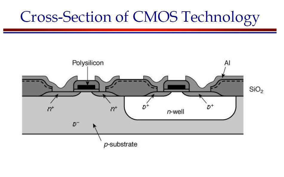
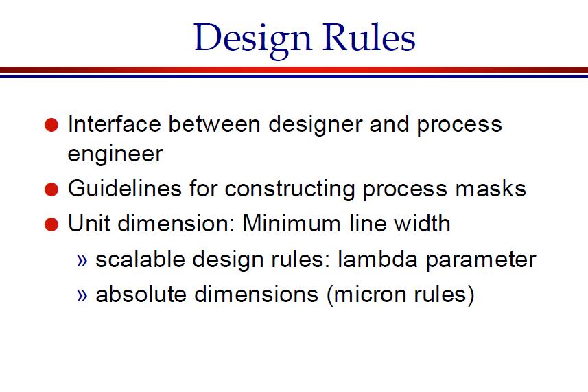
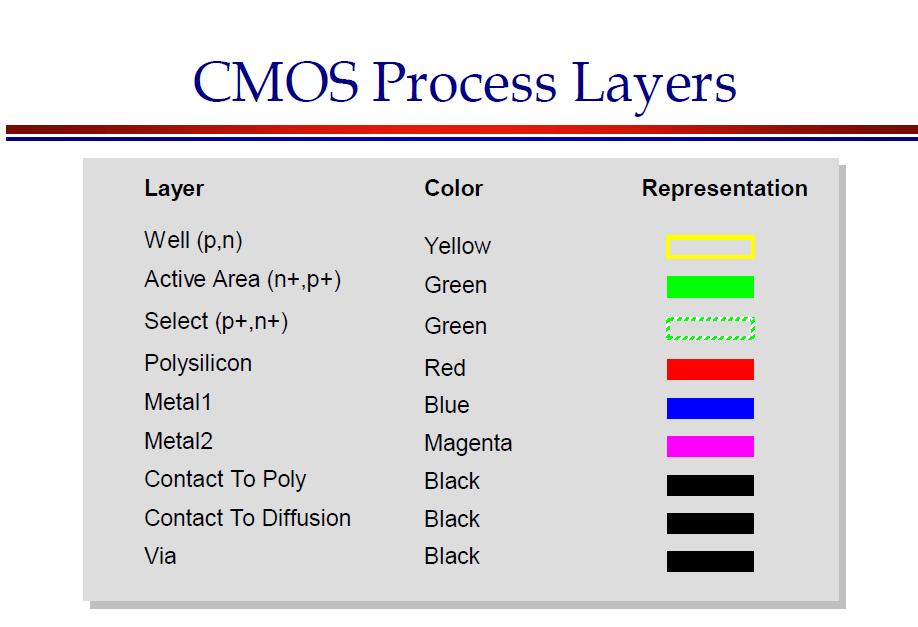
Microelectronics Part 1: Main CMOS circuits design rules
 GBM8320 Dispositifs Médicaux telligents Microelectronics Part 1: Main CMOS circuits design rules Mohamad Sawan et al. Laboratoire de neurotechnologies Polystim! http://www.cours.polymtl.ca/gbm8320/! med-amine.miled@polymtl.ca!
Practice 3: Semiconductors
 Practice 3: Semiconductors Digital Electronic Circuits Semester A 2012 VLSI Fabrication Process VLSI Very Large Scale Integration The ability to fabricate many devices on a single substrate within a given
Lecture 15: MOS Transistor models: Body effects, SPICE models. Context. In the last lecture, we discussed the modes of operation of a MOS FET:
 Lecture 15: MOS Transistor models: Body effects, SPICE models Context In the last lecture, we discussed the modes of operation of a MOS FET: oltage controlled resistor model I- curve (Square-Law Model)
SECTION: Circle one: Alam Lundstrom. ECE 305 Exam 5 SOLUTIONS: Spring 2016 April 18, 2016 M. A. Alam and M.S. Lundstrom Purdue University
 NAME: PUID: SECTION: Circle one: Alam Lundstrom ECE 305 Exam 5 SOLUTIONS: April 18, 2016 M A Alam and MS Lundstrom Purdue University This is a closed book exam You may use a calculator and the formula
Content. MIS Capacitor. Accumulation Depletion Inversion MOS CAPACITOR. A Cantoni Digital Switching
 Content MIS Capacitor Accumulation Depletion Inversion MOS CAPACITOR 1 MIS Capacitor Metal Oxide C ox p-si C s Components of a capacitance model for the MIS structure 2 MIS Capacitor- Accumulation ρ( x)
MOSFET Physics: The Long Channel Approximation
 MOSFET Physics: The ong Channel Approximation A basic n-channel MOSFET (Figure 1) consists of two heavily-doped n-type regions, the Source and Drain, that comprise the main terminals of the device. The
P. R. Nelson 1 ECE418 - VLSI. Midterm Exam. Solutions
 P. R. Nelson 1 ECE418 - VLSI Midterm Exam Solutions 1. (8 points) Draw the cross-section view for A-A. The cross-section view is as shown below.. ( points) Can you tell which of the metal1 regions is the
Lecture 7 PN Junction and MOS Electrostatics(IV) Metal Oxide Semiconductor Structure (contd.)
 Metal Oxide Semiconductor Structure (contd.)") Lecture 7 PN Junction and MOS Electrostatics(IV) Metal Oxide Semiconductor Structure (contd.) Outline 1. Overview of MOS electrostatics under bias 2. Depletion regime 3. Flatband 4. Accumulation regime
Lecture 7 PN Junction and MOS Electrostatics(IV) Metal Oxide Semiconductor Structure (contd.) Outline 1. Overview of MOS electrostatics under bias 2. Depletion regime 3. Flatband 4. Accumulation regime
ECE 546 Lecture 10 MOS Transistors
 ECE 546 Lecture 10 MOS Transistors Spring 2018 Jose E. Schutt-Aine Electrical & Computer Engineering University of Illinois jesa@illinois.edu NMOS Transistor NMOS Transistor N-Channel MOSFET Built on p-type
EE105 - Fall 2005 Microelectronic Devices and Circuits
 EE105 - Fall 005 Microelectronic Devices and Circuits ecture 7 MOS Transistor Announcements Homework 3, due today Homework 4 due next week ab this week Reading: Chapter 4 1 ecture Material ast lecture
Course Administration. CPE/EE 427, CPE 527 VLSI Design I L04: MOS Transistors. Review: CMOS Process at a Glance
 Course Administration CPE/EE 7, CPE 7 VLI esign I L: MO Transistors epartment of Electrical and Computer Engineering University of Alabama in Huntsville Aleksandar Milenkovic ( www.ece.uah.edu/~milenka
Semiconductor Physics fall 2012 problems
 Semiconductor Physics fall 2012 problems 1. An n-type sample of silicon has a uniform density N D = 10 16 atoms cm -3 of arsenic, and a p-type silicon sample has N A = 10 15 atoms cm -3 of boron. For each
VLSI Design I; A. Milenkovic 1
 Review: implified CMO Inverter Process CPE/EE 7, CPE 7 VLI esign I L: MO Transistor cut line epartment of Electrical and Computer Engineering University of Alabama in Huntsville Aleksandar Milenkovic (
Introduction and Background
 Analog CMOS Integrated Circuit Design Introduction and Background Dr. Jawdat Abu-Taha Department of Electrical and Computer Engineering Islamic University of Gaza jtaha@iugaza.edu.ps 1 Marking Assignments
MOS Transistor Properties Review
 MOS Transistor Properties Review 1 VLSI Chip Manufacturing Process Photolithography: transfer of mask patterns to the chip Diffusion or ion implantation: selective doping of Si substrate Oxidation: SiO
6.012 Electronic Devices and Circuits
 Page 1 of 12 YOUR NAME Department of Electrical Engineering and Computer Science Massachusetts Institute of Technology 6.012 Electronic Devices and Circuits FINAL EXAMINATION Open book. Notes: 1. Unless
1 Name: Student number: DEPARTMENT OF PHYSICS AND PHYSICAL OCEANOGRAPHY MEMORIAL UNIVERSITY OF NEWFOUNDLAND. Fall :00-11:00
 1 Name: DEPARTMENT OF PHYSICS AND PHYSICAL OCEANOGRAPHY MEMORIAL UNIVERSITY OF NEWFOUNDLAND Final Exam Physics 3000 December 11, 2012 Fall 2012 9:00-11:00 INSTRUCTIONS: 1. Answer all seven (7) questions.
ECEN474/704: (Analog) VLSI Circuit Design Spring 2018
 VLSI Circuit Design Spring 2018") ECEN474/704: (Analog) SI Circuit Design Spring 2018 ecture 2: MOS ransistor Modeling Sam Palermo Analog & Mixed-Signal Center exas A&M University Announcements If you haven t already, turn in your 0.18um
ECEN474/704: (Analog) SI Circuit Design Spring 2018 ecture 2: MOS ransistor Modeling Sam Palermo Analog & Mixed-Signal Center exas A&M University Announcements If you haven t already, turn in your 0.18um
MOS Transistor Theory
 CHAPTER 3 MOS Transistor Theory Outline 2 1. Introduction 2. Ideal I-V Characteristics 3. Nonideal I-V Effects 4. C-V Characteristics 5. DC Transfer Characteristics 6. Switch-level RC Delay Models MOS
ECE 305 Exam 5 SOLUTIONS: Spring 2015 April 17, 2015 Mark Lundstrom Purdue University
 NAME: PUID: : ECE 305 Exam 5 SOLUTIONS: April 17, 2015 Mark Lundstrom Purdue University This is a closed book exam. You may use a calculator and the formula sheet at the end of this exam. Following the
University of Pennsylvania Department of Electrical Engineering. ESE 570 Midterm Exam March 14, 2013 FORMULAS AND DATA
 University of Pennsylvania Department of Electrical Engineering ESE 570 Midterm Exam March 4, 03 FORMULAS AND DATA. PHYSICAL CONSTANTS: n i = intrinsic concentration undoped) silicon =.45 x 0 0 cm -3 @
ECE 340 Lecture 39 : MOS Capacitor II
 ECE 340 Lecture 39 : MOS Capacitor II Class Outline: Effects of Real Surfaces Threshold Voltage MOS Capacitance-Voltage Analysis Things you should know when you leave Key Questions What are the effects
Conduction in Semiconductors -Review
 Conduction in Semiconductors Review Intrinsic (undoped) Semiconductors intrinsic carrier concentration n i =.45x0 0 cm 3, at room temp. n = p = n i, in intrinsic (undoped) material n number of electrons,
Quantitative MOSFET. Step 1. Connect the MOS capacitor results for the electron charge in the inversion layer Q N to the drain current.
 Quantitative MOSFET Step 1. Connect the MOS capacitor results for the electron charge in the inversion layer Q N to the drain current. V DS _ n source polysilicon gate y = y * 0 x metal interconnect to
B.Supmonchai June 26, q Introduction of device basic equations. q Introduction of models for manual analysis.
 June 26, 2004 oal of this chapter Chapter 2 MO Transistor Theory oonchuay upmonchai Integrated esign Application Research (IAR) Laboratory June 16th, 2004; Revised June 16th, 2005 q Present intuitive understanding
UNIVERSITY OF CALIFORNIA College of Engineering Department of Electrical Engineering and Computer Sciences. EECS 130 Professor Ali Javey Fall 2006
 UNIVERSITY OF CALIFORNIA College of Engineering Department of Electrical Engineering and Computer Sciences EECS 130 Professor Ali Javey Fall 2006 Midterm 2 Name: SID: Closed book. Two sheets of notes are
Chapter 2 MOS Transistor theory
 Chapter MOS Transistor theory.1 Introduction An MOS transistor is a majority-carrier device, which the current a conductg channel between the source and the dra is modulated by a voltage applied to the
ECE-305: Fall 2017 MOS Capacitors and Transistors
 ECE-305: Fall 2017 MOS Capacitors and Transistors Pierret, Semiconductor Device Fundamentals (SDF) Chapters 15+16 (pp. 525-530, 563-599) Professor Peter Bermel Electrical and Computer Engineering Purdue
EECS130 Integrated Circuit Devices
 EECS130 Integrated Circuit Devices Professor Ali Javey 10/02/2007 MS Junctions, Lecture 2 MOS Cap, Lecture 1 Reading: finish chapter14, start chapter16 Announcements Professor Javey will hold his OH at
1. The MOS Transistor. Electrical Conduction in Solids
 Electrical Conduction in Solids!The band diagram describes the energy levels for electron in solids.!the lower filled band is named Valence Band.!The upper vacant band is named conduction band.!the distance
ESE370: Circuit-Level Modeling, Design, and Optimization for Digital Systems. Today. Refinement. Last Time. No Field. Body Contact
 ESE370: Circuit-Level Modeling, Design, and Optimization for Digital Systems Day 10: September 6, 01 MOS Transistor Basics Today MOS Transistor Topology Threshold Operating Regions Resistive Saturation
Metal-oxide-semiconductor field effect transistors (2 lectures)
") Metal-ide-semiconductor field effect transistors ( lectures) MOS physics (brief in book) Current-voltage characteristics - pinch-off / channel length modulation - weak inversion - velocity saturation -
Metal-ide-semiconductor field effect transistors ( lectures) MOS physics (brief in book) Current-voltage characteristics - pinch-off / channel length modulation - weak inversion - velocity saturation -
Chapter 4 Field-Effect Transistors
 Chapter 4 Field-Effect Transistors Microelectronic Circuit Design Richard C. Jaeger Travis N. Blalock 5/5/11 Chap 4-1 Chapter Goals Describe operation of MOSFETs. Define FET characteristics in operation
II III IV V VI B C N. Al Si P S. Zn Ga Ge As Se Cd In Sn Sb Te. Silicon (Si) the dominating material in IC manufacturing
 the dominating material in IC manufacturing") II III IV V VI B N Al Si P S Zn Ga Ge As Se d In Sn Sb Te Silicon (Si) the dominating material in I manufacturing ompound semiconductors III - V group: GaAs GaN GaSb GaP InAs InP InSb... The Energy Band
II III IV V VI B N Al Si P S Zn Ga Ge As Se d In Sn Sb Te Silicon (Si) the dominating material in I manufacturing ompound semiconductors III - V group: GaAs GaN GaSb GaP InAs InP InSb... The Energy Band
The Devices. Devices
 The The MOS Transistor Gate Oxyde Gate Source n+ Polysilicon Drain n+ Field-Oxyde (SiO 2 ) p-substrate p+ stopper Bulk Contact CROSS-SECTION of NMOS Transistor Cross-Section of CMOS Technology MOS transistors
Class 05: Device Physics II
 Topics: 1. Introduction 2. NFET Model and Cross Section with Parasitics 3. NFET as a Capacitor 4. Capacitance vs. Voltage Curves 5. NFET as a Capacitor - Band Diagrams at V=0 6. NFET as a Capacitor - Accumulation
The Gradual Channel Approximation for the MOSFET:
 6.01 - Electronic Devices and Circuits Fall 003 The Gradual Channel Approximation for the MOSFET: We are modeling the terminal characteristics of a MOSFET and thus want i D (v DS, v GS, v BS ), i B (v
MOS Transistor. EE141-Fall 2007 Digital Integrated Circuits. Review: What is a Transistor? Announcements. Class Material
 EE-Fall 7 igital Integrated Circuits MO Transistor Lecture MO Transistor Model Announcements Review: hat is a Transistor? Lab this week! Lab next week Homework # is due Thurs. Homework # due next Thurs.
Part 4: Heterojunctions - MOS Devices. MOSFET Current Voltage Characteristics
 MOS Device Uses: Part 4: Heterojunctions - MOS Devices MOSCAP capacitor: storing charge, charge-coupled device (CCD), etc. MOSFET transistor: switch, current amplifier, dynamic random access memory (DRAM-volatile),
ECE 497 JS Lecture - 12 Device Technologies
 ECE 497 JS Lecture - 12 Device Technologies Spring 2004 Jose E. Schutt-Aine Electrical & Computer Engineering University of Illinois jose@emlab.uiuc.edu 1 NMOS Transistor 2 ρ Source channel charge density
MOSFET Capacitance Model
 MOSFET Capacitance Model So far we discussed the MOSFET DC models. In real circuit operation, the device operates under time varying terminal voltages and the device operation can be described by: 1 small