MOSFET Physics: The Long Channel Approximation
|
|
|
- Ezra Dwayne Wilson
- 6 years ago
- Views:
Transcription
1 MOSFET Physics: The ong Channel Approximation A basic n-channel MOSFET (Figure 1) consists of two heavily-doped n-type regions, the Source and Drain, that comprise the main terminals of the device. The gate is made of heavily doped polysilicon, while the bulk of the device is p-type and is typically rather lightly doped. In much of what follows, we will assume that the substrate (bulk) terminal is at the same potential as the Source. However, it is extremely important to keep in mind that the substrate constitutes a fourth terminal, whose influence cannot always be ignored. FIGURE 1. n-channel MOSFET Gate Source Drain n-doped n-doped p-doped substrate bulk (substrate) As an increasing positive voltage is applied to the Gate, holes are progressively repelled away from the surface of the substrate. At some particular value of Gate voltage, denoted the threshold voltage (off), the surface becomes completely depleted of r charge. Further increases in Gate voltage induce an inversion layer, composed of electrons supplied by the Source (or Drain), that constitutes a conductive path ( channel ) between Source and Drain. The foregoing discussion implicitly assumes that the potential across the semiconductor surface is a constant, that is, there is zero Drain-to-Source voltage. ith this assumption, the induced inversion charge is proportional to the Gate voltage above the threshold, and the induced charge density is constant along the channel. However, if we do apply a positive Drain voltage, V, the channel potential must increase in some manner from zero at the Source end to V at the Drain end. The net voltage available to induce an inversion layer therefore decreases as one approaches the Drain end of the channel. Hence, we expect the induced channel charge density to vary from a maximum at the Source (where minus the channel potential is largest) to a minimum at the drain end of the channel (where minus the channel potential is smallest), as shown by the shaded region representing charge density in figure :
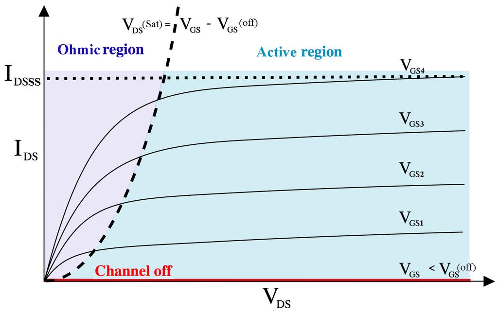
2 FIGURE. n-channel MOSFE T (shown at boundary between Ohmic region and Active region) gate source drain n+ n+ p-substrate bulk (substrate) Specifically, the channel charge density has the following form: ρ n ( x) { [ ] (off) (1) where ρ n (x) is the charge density at position x, is ε ox /t ox and V(x) is the channel potential at position x. e follow the convention of defining the x-direction as along the channel. Note also that is a capacitance per unit area. The minus sign simply reflects that the charge is made up of electrons in this nmos example. This last equation is all we really need to derive the most important equations governing the terminal characteristics. Drain Current in the Ohmic Region The Ohmic region of operation is defined as one in which is large enough (or V DS small enough) to guarantee the formation of an inversion layer the whole distance from source to drain. From our expression for the channel charge density, we see that it has a zero value when [ ] (off) 0 () The charge density thus first becomes zero at the drain end at some particular voltage. Therefore the boundary for the Ohmic region is defined by [ V DS ] (off) 0 V DS (off) V DSAT (3) As long as V DS is smaller than V DSAT, the device will be in the Ohmic region of operation.
3 Having derived an expression for the channel charge and defined the linear region of operation, we are now in a position to derive an expression for the device current in terms of the terminal variables. Current is proportional to charge times velocity, so we ve just about got it: ρ n ( x) v ( x) (4) The velocity at low fields (remember, this is the long channel approximation) is simply the product of mobility and electric field. Hence, ρ n ( x) E (5) where is the width of the device. Substituting now for the channel charge density, we get: [ (off) ] E (6) Next, we note that the (x-directed) electric field E is simply (minus) the gradient of the voltage along the channel. Therefore, dv [ (off) ] dx (7) so that dx [ (off) ] dv (8) Next, integrate along the channel and solve for : V DS dx [ (off) ] dv 0 0 (9) At last, we have the following expression for the Drain current in the Ohmic region: V DS [ V GS (off) ]V DS Note that the relationship between Drain current and Drain-to-Source voltage is nearly linear for small V DS. Thus, a MOSFET in the Ohmic region behaves as a voltage-controlled resistor. (10)
4 Drain Current in Saturation hen V DS is high enough so that the inversion layer does not extend all the way from Source to Drain, the channel is said to be pinched off. In this case, the channel charge ceases to increase, causing the total current to remain constant despite increases in V DS. Calculating the value of this current is easy; all we have to do is substitute V DSAT for V DS in our expression for current: V DSAT [ (off) ] V DSAT (11) which simplifies to: [ (off) ] (1) Hence, in saturation, the Drain current has a square-law dependence on the Gate-Source voltage, and is (ideally) independent of Drain voltage. The transconductance of such a device in saturation is easily found from differentiating our expression for drain current: g m [ (off) ] (13) which may also be expressed as: g m (14) Thus, a long-channel MOSFET s transconductance depends only on the square-root of the bias current.
5
MOSFET: Introduction
 E&CE 437 Integrated VLSI Systems MOS Transistor 1 of 30 MOSFET: Introduction Metal oxide semiconductor field effect transistor (MOSFET) or MOS is widely used for implementing digital designs Its major
ECE315 / ECE515 Lecture-2 Date:
 Lecture-2 Date: 04.08.2016 NMOS I/V Characteristics Discussion on I/V Characteristics MOSFET Second Order Effect NMOS I-V Characteristics ECE315 / ECE515 Gradual Channel Approximation: Cut-off Linear/Triode
ECE 342 Electronic Circuits. Lecture 6 MOS Transistors
 ECE 342 Electronic Circuits Lecture 6 MOS Transistors Jose E. Schutt-Aine Electrical & Computer Engineering University of Illinois jesa@illinois.edu 1 NMOS Transistor Typically L = 0.1 to 3 m, W = 0.2
Digital Integrated Circuits A Design Perspective. Jan M. Rabaey Anantha Chandrakasan Borivoje Nikolic. The Devices. July 30, Devices.
 Digital Integrated Circuits A Design Perspective Jan M. Rabaey Anantha Chandrakasan Borivoje Nikolic The July 30, 2002 1 Goal of this chapter Present intuitive understanding of device operation Introduction
Practice 3: Semiconductors
 Practice 3: Semiconductors Digital Electronic Circuits Semester A 2012 VLSI Fabrication Process VLSI Very Large Scale Integration The ability to fabricate many devices on a single substrate within a given
Lecture 9 MOSFET(II) MOSFET I V CHARACTERISTICS(contd.)
 MOSFET I V CHARACTERISTICS(contd.)") Lecture 9 MOSFET(II) MOSFET I V CHARACTERISTICS(contd.) Outline 1. The saturation region 2. Backgate characteristics Reading Assignment: Howe and Sodini, Chapter 4, Section 4.4 6.012 Spring 2009 Lecture
Lecture 9 MOSFET(II) MOSFET I V CHARACTERISTICS(contd.) Outline 1. The saturation region 2. Backgate characteristics Reading Assignment: Howe and Sodini, Chapter 4, Section 4.4 6.012 Spring 2009 Lecture
MOS Transistor Properties Review
 MOS Transistor Properties Review 1 VLSI Chip Manufacturing Process Photolithography: transfer of mask patterns to the chip Diffusion or ion implantation: selective doping of Si substrate Oxidation: SiO
The Devices. Digital Integrated Circuits A Design Perspective. Jan M. Rabaey Anantha Chandrakasan Borivoje Nikolic. July 30, 2002
 Digital Integrated Circuits A Design Perspective Jan M. Rabaey Anantha Chandrakasan Borivoje Nikolic The Devices July 30, 2002 Goal of this chapter Present intuitive understanding of device operation Introduction
Lecture 12: MOSFET Devices
 Lecture 12: MOSFET Devices Gu-Yeon Wei Division of Engineering and Applied Sciences Harvard University guyeon@eecs.harvard.edu Wei 1 Overview Reading S&S: Chapter 5.1~5.4 Supplemental Reading Background
MOS Transistor I-V Characteristics and Parasitics
 ECEN454 Digital Integrated Circuit Design MOS Transistor I-V Characteristics and Parasitics ECEN 454 Facts about Transistors So far, we have treated transistors as ideal switches An ON transistor passes
MOS Transistors. Prof. Krishna Saraswat. Department of Electrical Engineering Stanford University Stanford, CA
 MOS Transistors Prof. Krishna Saraswat Department of Electrical Engineering S Stanford, CA 94305 saraswat@stanford.edu 1 1930: Patent on the Field-Effect Transistor! Julius Lilienfeld filed a patent describing
Integrated Circuits & Systems
 Federal University of Santa Catarina Center for Technology Computer Science & Electronics Engineering Integrated Circuits & Systems INE 5442 Lecture 10 MOSFET part 1 guntzel@inf.ufsc.br ual-well Trench-Isolated
Chapter 4 Field-Effect Transistors
 Chapter 4 Field-Effect Transistors Microelectronic Circuit Design Richard C. Jaeger Travis N. Blalock 5/5/11 Chap 4-1 Chapter Goals Describe operation of MOSFETs. Define FET characteristics in operation
Lecture 3: CMOS Transistor Theory
 Lecture 3: CMOS Transistor Theory Outline Introduction MOS Capacitor nmos I-V Characteristics pmos I-V Characteristics Gate and Diffusion Capacitance 2 Introduction So far, we have treated transistors
Lecture 11: J-FET and MOSFET
 ENE 311 Lecture 11: J-FET and MOSFET FETs vs. BJTs Similarities: Amplifiers Switching devices Impedance matching circuits Differences: FETs are voltage controlled devices. BJTs are current controlled devices.
ECE-305: Fall 2017 MOS Capacitors and Transistors
 ECE-305: Fall 2017 MOS Capacitors and Transistors Pierret, Semiconductor Device Fundamentals (SDF) Chapters 15+16 (pp. 525-530, 563-599) Professor Peter Bermel Electrical and Computer Engineering Purdue
CMPEN 411 VLSI Digital Circuits. Lecture 03: MOS Transistor
 CMPEN 411 VLSI Digital Circuits Lecture 03: MOS Transistor Kyusun Choi [Adapted from Rabaey s Digital Integrated Circuits, Second Edition, 2003 J. Rabaey, A. Chandrakasan, B. Nikolic] CMPEN 411 L03 S.1
MOS Transistor Theory
 MOS Transistor Theory So far, we have viewed a MOS transistor as an ideal switch (digital operation) Reality: less than ideal EE 261 Krish Chakrabarty 1 Introduction So far, we have treated transistors
Microelectronics Part 1: Main CMOS circuits design rules
 GBM8320 Dispositifs Médicaux telligents Microelectronics Part 1: Main CMOS circuits design rules Mohamad Sawan et al. Laboratoire de neurotechnologies Polystim! http://www.cours.polymtl.ca/gbm8320/! med-amine.miled@polymtl.ca!
SECTION: Circle one: Alam Lundstrom. ECE 305 Exam 5 SOLUTIONS: Spring 2016 April 18, 2016 M. A. Alam and M.S. Lundstrom Purdue University
 NAME: PUID: SECTION: Circle one: Alam Lundstrom ECE 305 Exam 5 SOLUTIONS: April 18, 2016 M A Alam and MS Lundstrom Purdue University This is a closed book exam You may use a calculator and the formula
FIELD-EFFECT TRANSISTORS
 FIEL-EFFECT TRANSISTORS 1 Semiconductor review 2 The MOS capacitor 2 The enhancement-type N-MOS transistor 3 I-V characteristics of enhancement MOSFETS 4 The output characteristic of the MOSFET in saturation
Device Models (PN Diode, MOSFET )
") Device Models (PN Diode, MOSFET ) Instructor: Steven P. Levitan steve@ece.pitt.edu TA: Gayatri Mehta, José Martínez Book: Digital Integrated Circuits: A Design Perspective; Jan Rabaey Lab Notes: Handed
Device Models (PN Diode, MOSFET ) Instructor: Steven P. Levitan steve@ece.pitt.edu TA: Gayatri Mehta, José Martínez Book: Digital Integrated Circuits: A Design Perspective; Jan Rabaey Lab Notes: Handed
MOS Capacitors ECE 2204
 MOS apacitors EE 2204 Some lasses of Field Effect Transistors Metal-Oxide-Semiconductor Field Effect Transistor MOSFET, which will be the type that we will study in this course. Metal-Semiconductor Field
EE105 - Fall 2005 Microelectronic Devices and Circuits
 EE105 - Fall 005 Microelectronic Devices and Circuits ecture 7 MOS Transistor Announcements Homework 3, due today Homework 4 due next week ab this week Reading: Chapter 4 1 ecture Material ast lecture
Lecture 4: CMOS Transistor Theory
 Introduction to CMOS VLSI Design Lecture 4: CMOS Transistor Theory David Harris, Harvey Mudd College Kartik Mohanram and Steven Levitan University of Pittsburgh Outline q Introduction q MOS Capacitor q
Introduction to CMOS VLSI. Chapter 2: CMOS Transistor Theory. Harris, 2004 Updated by Li Chen, Outline
 Introduction to MOS VLSI Design hapter : MOS Transistor Theory copyright@david Harris, 004 Updated by Li hen, 010 Outline Introduction MOS apacitor nmos IV haracteristics pmos IV haracteristics Gate and
Lecture 15: MOS Transistor models: Body effects, SPICE models. Context. In the last lecture, we discussed the modes of operation of a MOS FET:
 Lecture 15: MOS Transistor models: Body effects, SPICE models Context In the last lecture, we discussed the modes of operation of a MOS FET: oltage controlled resistor model I- curve (Square-Law Model)
Lecture 15 OUTLINE. MOSFET structure & operation (qualitative) Review of electrostatics The (N)MOS capacitor
 Review of electrostatics The (N)MOS capacitor") Lecture 15 OUTLINE MOSFET structure & operation (qualitative) Review of electrostatics The (N)MOS capacitor Electrostatics Charge vs. voltage characteristic Reading: Chapter 6.1 6.2.1 EE15 Spring 28 Lecture
Lecture 15 OUTLINE MOSFET structure & operation (qualitative) Review of electrostatics The (N)MOS capacitor Electrostatics Charge vs. voltage characteristic Reading: Chapter 6.1 6.2.1 EE15 Spring 28 Lecture
6.012 MICROELECTRONIC DEVICES AND CIRCUITS
 MASSACHUSETTS INSTITUTE OF TECHNOLOGY Department of Electrical Engineering and Computer Science 6.012 MICROELECTRONIC DEVICES AND CIRCUITS Answers to Exam 2 Spring 2008 Problem 1: Graded by Prof. Fonstad
ESE 570: Digital Integrated Circuits and VLSI Fundamentals
 ESE 570: Digital Integrated Circuits and VLSI Fundamentals Lec 4: January 23, 2018 MOS Transistor Theory, MOS Model Penn ESE 570 Spring 2018 Khanna Lecture Outline! CMOS Process Enhancements! Semiconductor
Chapter 6: Field-Effect Transistors
 Chapter 6: Field-Effect Transistors slamic University of Gaza Dr. Talal Skaik FETs vs. BJTs Similarities: Amplifiers Switching devices mpedance matching circuits Differences: FETs are voltage controlled
Lecture 15 OUTLINE. MOSFET structure & operation (qualitative) Review of electrostatics The (N)MOS capacitor
 Review of electrostatics The (N)MOS capacitor") Lecture 15 OUTLINE MOSFET structure & operation (qualitative) Review of electrostatics The (N)MOS capacitor Electrostatics t ti Charge vs. voltage characteristic Reading: Chapter 6.1 6.2.1 EE105 Fall 2007
Lecture 15 OUTLINE MOSFET structure & operation (qualitative) Review of electrostatics The (N)MOS capacitor Electrostatics t ti Charge vs. voltage characteristic Reading: Chapter 6.1 6.2.1 EE105 Fall 2007
EEC 118 Lecture #2: MOSFET Structure and Basic Operation. Rajeevan Amirtharajah University of California, Davis Jeff Parkhurst Intel Corporation
 EEC 118 Lecture #2: MOSFET Structure and Basic Operation Rajeevan Amirtharajah University of California, Davis Jeff Parkhurst Intel Corporation Announcements Lab 1 this week, report due next week Bring
ECEN474/704: (Analog) VLSI Circuit Design Spring 2018
 VLSI Circuit Design Spring 2018") ECEN474/704: (Analog) SI Circuit Design Spring 2018 ecture 2: MOS ransistor Modeling Sam Palermo Analog & Mixed-Signal Center exas A&M University Announcements If you haven t already, turn in your 0.18um
ECEN474/704: (Analog) SI Circuit Design Spring 2018 ecture 2: MOS ransistor Modeling Sam Palermo Analog & Mixed-Signal Center exas A&M University Announcements If you haven t already, turn in your 0.18um
! PN Junction. ! MOS Transistor Topology. ! Threshold. ! Operating Regions. " Resistive. " Saturation. " Subthreshold (next class)
") ESE370: ircuitlevel Modeling, Design, and Optimization for Digital Systems Lec 7: September 20, 2017 MOS Transistor Operating Regions Part 1 Today! PN Junction! MOS Transistor Topology! Threshold! Operating
ESE370: ircuitlevel Modeling, Design, and Optimization for Digital Systems Lec 7: September 20, 2017 MOS Transistor Operating Regions Part 1 Today! PN Junction! MOS Transistor Topology! Threshold! Operating
The Devices: MOS Transistors
 The Devices: MOS Transistors References: Semiconductor Device Fundamentals, R. F. Pierret, Addison-Wesley Digital Integrated Circuits: A Design Perspective, J. Rabaey et.al. Prentice Hall NMOS Transistor
Fundamentals of the Metal Oxide Semiconductor Field-Effect Transistor
 Triode Working FET Fundamentals of the Metal Oxide Semiconductor Field-Effect Transistor The characteristics of energy bands as a function of applied voltage. Surface inversion. The expression for the
Typical example of the FET: MEtal Semiconductor FET (MESFET)
") Typical example of the FET: MEtal Semiconductor FET (MESFET) Conducting channel (RED) is made of highly doped material. The electron concentration in the channel n = the donor impurity concentration N
Typical example of the FET: MEtal Semiconductor FET (MESFET) Conducting channel (RED) is made of highly doped material. The electron concentration in the channel n = the donor impurity concentration N
Today s lecture. EE141- Spring 2003 Lecture 4. Design Rules CMOS Inverter MOS Transistor Model
 - Spring 003 Lecture 4 Design Rules CMOS Inverter MOS Transistor Model Today s lecture Design Rules The CMOS inverter at a glance An MOS transistor model for manual analysis Important! Labs start next
II III IV V VI B C N. Al Si P S. Zn Ga Ge As Se Cd In Sn Sb Te. Silicon (Si) the dominating material in IC manufacturing
 the dominating material in IC manufacturing") II III IV V VI B N Al Si P S Zn Ga Ge As Se d In Sn Sb Te Silicon (Si) the dominating material in I manufacturing ompound semiconductors III - V group: GaAs GaN GaSb GaP InAs InP InSb... The Energy Band
II III IV V VI B N Al Si P S Zn Ga Ge As Se d In Sn Sb Te Silicon (Si) the dominating material in I manufacturing ompound semiconductors III - V group: GaAs GaN GaSb GaP InAs InP InSb... The Energy Band
EE105 - Fall 2006 Microelectronic Devices and Circuits
 EE105 - Fall 2006 Microelectronic Devices and Circuits Prof. Jan M. Rabaey (jan@eecs) Lecture 7: MOS Transistor Some Administrative Issues Lab 2 this week Hw 2 due on We Hw 3 will be posted same day MIDTERM
Fig. 1 CMOS Transistor Circuits (a) Inverter Out = NOT In, (b) NOR-gate C = NOT (A or B)
 Inverter Out = NOT In, (b) NOR-gate C = NOT (A or B)") 1 Introduction to Transistor-Level Logic Circuits 1 By Prawat Nagvajara At the transistor level of logic circuits, transistors operate as switches with the logic variables controlling the open or closed
1 Introduction to Transistor-Level Logic Circuits 1 By Prawat Nagvajara At the transistor level of logic circuits, transistors operate as switches with the logic variables controlling the open or closed
ECE 342 Electronic Circuits. 3. MOS Transistors
 ECE 342 Electronic Circuits 3. MOS Transistors Jose E. Schutt-Aine Electrical & Computer Engineering University of Illinois jschutt@emlab.uiuc.edu 1 NMOS Transistor Typically L = 0.1 to 3 m, W = 0.2 to
CMOS INVERTER. Last Lecture. Metrics for qualifying digital circuits. »Cost» Reliability» Speed (delay)»performance
»performance") CMOS INVERTER Last Lecture Metrics for qualifying digital circuits»cost» Reliability» Speed (delay)»performance 1 Today s lecture The CMOS inverter at a glance An MOS transistor model for manual analysis
CMOS INVERTER Last Lecture Metrics for qualifying digital circuits»cost» Reliability» Speed (delay)»performance 1 Today s lecture The CMOS inverter at a glance An MOS transistor model for manual analysis
Lecture 10 MOSFET (III) MOSFET Equivalent Circuit Models
 MOSFET Equivalent Circuit Models") Lecture 10 MOSFET (III) MOSFET Equivalent Circuit Models Outline Lowfrequency smallsignal equivalent circuit model Highfrequency smallsignal equivalent circuit model Reading Assignment: Howe and Sodini;
Lecture 10 MOSFET (III) MOSFET Equivalent Circuit Models Outline Lowfrequency smallsignal equivalent circuit model Highfrequency smallsignal equivalent circuit model Reading Assignment: Howe and Sodini;
N Channel MOSFET level 3
 N Channel MOSFET level 3 mosn3 NSource NBulk NSource NBulk NSource NBulk NSource (a) (b) (c) (d) NBulk Figure 1: MOSFET Types Form: mosn3: instance name n 1 n n 3 n n 1 is the drain node, n is the gate
MOSFET Capacitance Model
 MOSFET Capacitance Model So far we discussed the MOSFET DC models. In real circuit operation, the device operates under time varying terminal voltages and the device operation can be described by: 1 small
Electronic Circuits 1. Transistor Devices. Contents BJT and FET Characteristics Operations. Prof. C.K. Tse: Transistor devices
 Electronic Circuits 1 Transistor Devices Contents BJT and FET Characteristics Operations 1 What is a transistor? Three-terminal device whose voltage-current relationship is controlled by a third voltage
LECTURE 3 MOSFETS II. MOS SCALING What is Scaling?
 LECTURE 3 MOSFETS II Lecture 3 Goals* * Understand constant field and constant voltage scaling and their effects. Understand small geometry effects for MOS transistors and their implications modeling and
ESE 570: Digital Integrated Circuits and VLSI Fundamentals
 ESE 570: Digital Integrated Circuits and VLSI Fundamentals Lec 5: January 25, 2018 MOS Operating Regions, pt. 1 Lecture Outline! 3 Regions of operation for MOSFET " Subthreshold " Linear " Saturation!
Lecture 5: CMOS Transistor Theory
 Lecture 5: CMOS Transistor Theory Slides courtesy of Deming Chen Slides based on the initial set from David Harris CMOS VLSI Design Outline q q q q q q q Introduction MOS Capacitor nmos I-V Characteristics
ELEC 3908, Physical Electronics, Lecture 23. The MOSFET Square Law Model
 ELEC 3908, Physical Electronics, Lecture 23 The MOSFET Square Law Model Lecture Outline As with the diode and bipolar, have looked at basic structure of the MOSFET and now turn to derivation of a current
Lecture 11: MOS Transistor
 Lecture 11: MOS Transistor Prof. Niknejad Lecture Outline Review: MOS Capacitors Regions MOS Capacitors (3.8 3.9) CV Curve Threshold Voltage MOS Transistors (4.1 4.3): Overview Cross-section and layout
Lecture Outline. ESE 570: Digital Integrated Circuits and VLSI Fundamentals. Review: MOS Capacitor with External Bias
 ESE 57: Digital Integrated Circuits and VLSI Fundamentals Lec 5: Januar 6, 17 MOS Operating Regions, pt. 1 Lecture Outline! 3 Regions of operation for MOSFET " Subthreshold " Linear " Saturation! Level
Lecture 3: Transistor as an thermonic switch
 Lecture 3: Transistor as an thermonic switch 2016-01-21 Lecture 3, High Speed Devices 2016 1 Lecture 3: Transistors as an thermionic switch Reading Guide: 54-57 in Jena Transistor metrics Reservoir equilibrium
Lecture #25. Due in class (5 PM) on Thursday May 1 st. 20 pt penalty for late submissions, accepted until 5 PM on 5/8
 on Thursday May 1 st. 20 pt penalty for late submissions, accepted until 5 PM on 5/8") ecture #5 Design Project: Due in class (5 PM on hursday May 1 st 0 pt penalty for late submissions, accepted until 5 PM on 5/8 Your J design does not need to meet the performance specifications when and
ecture #5 Design Project: Due in class (5 PM on hursday May 1 st 0 pt penalty for late submissions, accepted until 5 PM on 5/8 Your J design does not need to meet the performance specifications when and
Lecture 12: MOS Capacitors, transistors. Context
 Lecture 12: MOS Capacitors, transistors Context In the last lecture, we discussed PN diodes, and the depletion layer into semiconductor surfaces. Small signal models In this lecture, we will apply those
MOS CAPACITOR AND MOSFET
 EE336 Semiconductor Devices 1 MOS CAPACITOR AND MOSFET Dr. Mohammed M. Farag Ideal MOS Capacitor Semiconductor Devices Physics and Technology Chapter 5 EE336 Semiconductor Devices 2 MOS Capacitor Structure
Semiconductor Physics fall 2012 problems
 Semiconductor Physics fall 2012 problems 1. An n-type sample of silicon has a uniform density N D = 10 16 atoms cm -3 of arsenic, and a p-type silicon sample has N A = 10 15 atoms cm -3 of boron. For each
Introduction and Background
 Analog CMOS Integrated Circuit Design Introduction and Background Dr. Jawdat Abu-Taha Department of Electrical and Computer Engineering Islamic University of Gaza jtaha@iugaza.edu.ps 1 Marking Assignments
ELEC 3908, Physical Electronics, Lecture 26. MOSFET Small Signal Modelling
 ELEC 3908, Physical Electronics, Lecture 26 MOSFET Small Signal Modelling Lecture Outline MOSFET small signal behavior will be considered in the same way as for the diode and BJT Capacitances will be considered
! CMOS Process Enhancements. ! Semiconductor Physics. " Band gaps. " Field Effects. ! MOS Physics. " Cut-off. " Depletion.
 ESE 570: Digital Integrated Circuits and VLSI Fundamentals Lec 4: January 3, 018 MOS Transistor Theory, MOS Model Lecture Outline! CMOS Process Enhancements! Semiconductor Physics " Band gaps " Field Effects!
EE 560 MOS TRANSISTOR THEORY
 1 EE 560 MOS TRANSISTOR THEORY PART 1 TWO TERMINAL MOS STRUCTURE V G (GATE VOLTAGE) 2 GATE OXIDE SiO 2 SUBSTRATE p-type doped Si (N A = 10 15 to 10 16 cm -3 ) t ox V B (SUBSTRATE VOLTAGE) EQUILIBRIUM:
HW 5 posted due in two weeks Lab this week Midterm graded Project to be launched in week 7
 HW 5 posted due in two weeks Lab this week Midterm graded Project to be launched in week 7 2 What do digital IC designers need to know? 5 EE4 EECS4 6 3 0< V GS - V T < V DS Pinch-off 7 For (V GS V T )
Lecture 04 Review of MOSFET
 ECE 541/ME 541 Microelectronic Fabrication Techniques Lecture 04 Review of MOSFET Zheng Yang (ERF 3017, email: yangzhen@uic.edu) What is a Transistor? A Switch! An MOS Transistor V GS V T V GS S Ron D
Electronics Fets and Mosfets Prof D C Dube Department of Physics Indian Institute of Technology, Delhi
 Electronics Fets and Mosfets Prof D C Dube Department of Physics Indian Institute of Technology, Delhi Module No. #05 Lecture No. #02 FETS and MOSFETS (contd.) In the previous lecture, we studied the working
Lecture 10 MOSFET (III) MOSFET Equivalent Circuit Models
 MOSFET Equivalent Circuit Models") Lecture 1 MOSFET (III) MOSFET Equivalent Circuit Models Outline Lowfrequency smallsignal equivalent circuit model Highfrequency smallsignal equivalent circuit model Reading Assignment: Howe and Sodini;
Lecture 1 MOSFET (III) MOSFET Equivalent Circuit Models Outline Lowfrequency smallsignal equivalent circuit model Highfrequency smallsignal equivalent circuit model Reading Assignment: Howe and Sodini;
EE105 Fall 2014 Microelectronic Devices and Circuits. NMOS Transistor Capacitances: Saturation Region
 EE105 Fall 014 Microelectronic Devices and Circuits Prof. Ming C. Wu wu@eecs.berkeley.edu 511 Sutardja Dai Hall (SDH) 1 NMOS Transistor Capacitances: Saturation Region Drain no longer connected to channel
ESE 570: Digital Integrated Circuits and VLSI Fundamentals
 ESE 570: Digital Integrated Circuits and VLSI Fundamentals Lec 4: January 24, 2017 MOS Transistor Theory, MOS Model Penn ESE 570 Spring 2017 Khanna Lecture Outline! Semiconductor Physics " Band gaps "
Chapter 5 MOSFET Theory for Submicron Technology
 Chapter 5 MOSFET Theory for Submicron Technology Short channel effects Other small geometry effects Parasitic components Velocity saturation/overshoot Hot carrier effects ** Majority of these notes are
MOSFET. Id-Vd curve. I DS Transfer curve V G. Lec. 8. Vd=1V. Saturation region. V Th
 MOSFET Id-Vd curve Saturation region I DS Transfer curve Vd=1V V Th V G 1 0 < V GS < V T V GS > V T V Gs >V T & Small V D > 0 I DS WQ inv WC v WC i V V VDS V V G i T G n T L n I D g V D (g conductance
Current mechanisms Exam January 27, 2012
 Current mechanisms Exam January 27, 2012 There are four mechanisms that typically cause currents to flow: thermionic emission, diffusion, drift, and tunneling. Explain briefly which kind of current mechanisms
Section 12: Intro to Devices
 Section 12: Intro to Devices Extensive reading materials on reserve, including Robert F. Pierret, Semiconductor Device Fundamentals EE143 Ali Javey Bond Model of Electrons and Holes Si Si Si Si Si Si Si
Quantitative MOSFET. Step 1. Connect the MOS capacitor results for the electron charge in the inversion layer Q N to the drain current.
 Quantitative MOSFET Step 1. Connect the MOS capacitor results for the electron charge in the inversion layer Q N to the drain current. V DS _ n source polysilicon gate y = y * 0 x metal interconnect to
Lecture 30 The Short Metal Oxide Semiconductor Field Effect Transistor. November 15, 2002
 6.720J/3.43J Integrated Microelectronic Devices Fall 2002 Lecture 30 1 Lecture 30 The Short Metal Oxide Semiconductor Field Effect Transistor November 15, 2002 Contents: 1. Short channel effects Reading
Final Examination EE 130 December 16, 1997 Time allotted: 180 minutes
 Final Examination EE 130 December 16, 1997 Time allotted: 180 minutes Problem 1: Semiconductor Fundamentals [30 points] A uniformly doped silicon sample of length 100µm and cross-sectional area 100µm 2
Long Channel MOS Transistors
 Long Channel MOS Transistors The theory developed for MOS capacitor (HO #2) can be directly extended to Metal-Oxide-Semiconductor Field-Effect transistors (MOSFET) by considering the following structure:
The Gradual Channel Approximation for the MOSFET:
 6.01 - Electronic Devices and Circuits Fall 003 The Gradual Channel Approximation for the MOSFET: We are modeling the terminal characteristics of a MOSFET and thus want i D (v DS, v GS, v BS ), i B (v
MOS Capacitor MOSFET Devices. MOSFET s. INEL Solid State Electronics. Manuel Toledo Quiñones. ECE Dept. UPRM.
 INEL 6055 - Solid State Electronics ECE Dept. UPRM 20th March 2006 Definitions MOS Capacitor Isolated Metal, SiO 2, Si Threshold Voltage qφ m metal d vacuum level SiO qχ 2 E g /2 qφ F E C E i E F E v qφ
Field effect = Induction of an electronic charge due to an electric field Example: Planar capacitor
 JFETs AND MESFETs Introduction Field effect = Induction of an electronic charge due to an electric field Example: Planar capacitor Why would an FET made of a planar capacitor with two metal plates, as
ECE 546 Lecture 10 MOS Transistors
 ECE 546 Lecture 10 MOS Transistors Spring 2018 Jose E. Schutt-Aine Electrical & Computer Engineering University of Illinois jesa@illinois.edu NMOS Transistor NMOS Transistor N-Channel MOSFET Built on p-type
ESE370: Circuit-Level Modeling, Design, and Optimization for Digital Systems. Today. Refinement. Last Time. No Field. Body Contact
 ESE370: Circuit-Level Modeling, Design, and Optimization for Digital Systems Day 10: September 6, 01 MOS Transistor Basics Today MOS Transistor Topology Threshold Operating Regions Resistive Saturation
ESE 570: Digital Integrated Circuits and VLSI Fundamentals
 ESE 570: Digital Integrated Circuits and VLSI Fundamentals Lec 4: January 29, 2019 MOS Transistor Theory, MOS Model Penn ESE 570 Spring 2019 Khanna Lecture Outline! CMOS Process Enhancements! Semiconductor
Metal-Oxide-Semiconductor Field Effect Transistor (MOSFET)
") Metal-Oxide-Semiconductor ield Effect Transistor (MOSET) Source Gate Drain p p n- substrate - SUB MOSET is a symmetrical device in the most general case (for example, in an integrating circuit) In a separate
Metal-Oxide-Semiconductor ield Effect Transistor (MOSET) Source Gate Drain p p n- substrate - SUB MOSET is a symmetrical device in the most general case (for example, in an integrating circuit) In a separate
Lecture 28 - The Long Metal-Oxide-Semiconductor Field-Effect Transistor (cont.) April 18, 2007
 April 18, 2007") 6.720J/3.43J - Integrated Microelectronic Devices - Spring 2007 Lecture 28-1 Lecture 28 - The Long Metal-Oxide-Semiconductor Field-Effect Transistor (cont.) April 18, 2007 Contents: 1. Second-order and
6.720J/3.43J - Integrated Microelectronic Devices - Spring 2007 Lecture 28-1 Lecture 28 - The Long Metal-Oxide-Semiconductor Field-Effect Transistor (cont.) April 18, 2007 Contents: 1. Second-order and
EE105 - Fall 2006 Microelectronic Devices and Circuits. Some Administrative Issues
 EE105 - Fall 006 Microelectronic evices and Circuits Prof. Jan M. Rabaey (jan@eecs Lecture 8: MOS Small Signal Model Some Administrative Issues REIEW Session Next Week Tu Sept 6 6:00-7:30pm; 060 alley
ECE-305: Spring 2016 MOSFET IV
 ECE-305: Spring 2016 MOSFET IV Professor Mark Lundstrom Electrical and Computer Engineering Purdue University, West Lafayette, IN USA lundstro@purdue.edu Lundstrom s lecture notes: Lecture 4 4/7/16 outline
Operation and Modeling of. The MOS Transistor. Second Edition. Yannis Tsividis Columbia University. New York Oxford OXFORD UNIVERSITY PRESS
 Operation and Modeling of The MOS Transistor Second Edition Yannis Tsividis Columbia University New York Oxford OXFORD UNIVERSITY PRESS CONTENTS Chapter 1 l.l 1.2 1.3 1.4 1.5 1.6 1.7 Chapter 2 2.1 2.2
Transistors - a primer
 ransistors - a primer What is a transistor? Solid-state triode - three-terminal device, with voltage (or current) at third terminal used to control current between other two terminals. wo types: bipolar
JFET Operating Characteristics: V GS = 0 V 14. JFET Operating Characteristics: V GS = 0 V 15
 J Operating Characteristics: V GS = 0 V 14 V GS = 0 and V DS increases from 0 to a more positive voltage: Gate and Source terminals: at the same potential Drain: at positive potential => reverse biased
The Devices. Digital Integrated Circuits A Design Perspective. Jan M. Rabaey Anantha Chandrakasan Borivoje Nikolic. July 30, 2002
 igital Integrated Circuits A esign Perspective Jan M. Rabaey Anantha Chandrakasan Borivoje Nikolic The evices July 30, 2002 Goal of this chapter Present intuitive understanding of device operation Introduction
The Intrinsic Silicon
 The Intrinsic ilicon Thermally generated electrons and holes Carrier concentration p i =n i ni=1.45x10 10 cm-3 @ room temp Generally: n i = 3.1X10 16 T 3/2 e -1.21/2KT cm -3 T= temperature in K o (egrees
6.012 Electronic Devices and Circuits Spring 2005
 6.012 Electronic Devices and Circuits Spring 2005 May 16, 2005 Final Exam (200 points) -OPEN BOOK- Problem NAME RECITATION TIME 1 2 3 4 5 Total General guidelines (please read carefully before starting):
Extensive reading materials on reserve, including
 Section 12: Intro to Devices Extensive reading materials on reserve, including Robert F. Pierret, Semiconductor Device Fundamentals EE143 Ali Javey Bond Model of Electrons and Holes Si Si Si Si Si Si Si
Section 12: Intro to Devices
 Section 12: Intro to Devices Extensive reading materials on reserve, including Robert F. Pierret, Semiconductor Device Fundamentals Bond Model of Electrons and Holes Si Si Si Si Si Si Si Si Si Silicon
Charge Storage in the MOS Structure. The Inverted MOS Capacitor (V GB > V Tn )
") The Inverted MO Capacitor (V > V Tn ) We consider the surface potential as Þxed (ÒpinnedÓ) at φ s,max = - φ p φ(x).5 V. V V ox Charge torage in the MO tructure Three regions of operation: Accumulation:
The Inverted MO Capacitor (V > V Tn ) We consider the surface potential as Þxed (ÒpinnedÓ) at φ s,max = - φ p φ(x).5 V. V V ox Charge torage in the MO tructure Three regions of operation: Accumulation:
ECE 305: Fall MOSFET Energy Bands
 ECE 305: Fall 2016 MOSFET Energy Bands Professor Peter Bermel Electrical and Computer Engineering Purdue University, West Lafayette, IN USA pbermel@purdue.edu Pierret, Semiconductor Device Fundamentals
Long-channel MOSFET IV Corrections
 Long-channel MOSFET IV orrections Three MITs of the Day The body ect and its influence on long-channel V th. Long-channel subthreshold conduction and control (subthreshold slope S) Scattering components
MOSFET Model with Simple Extraction Procedures, Suitable for Sensitive Analog Simulations
 ROMANIAN JOURNAL OF INFORMATION SCIENCE AND TECHNOLOGY Volume 10, Number 2, 2007, 189 197 MOSFET Model with Simple Extraction Procedures, Suitable for Sensitive Analog Simulations S. EFTIMIE 1, ALEX. RUSU