Electrical Characteristics of MOS Devices
|
|
|
- Janel Clark
- 6 years ago
- Views:
Transcription
1 Electrical Characteristics of MOS Devices The MOS Capacitor Voltage components Accumulation, Depletion, Inversion Modes Effect of channel bias and substrate bias Effect of gate oide charges Threshold-voltage adjustment by implantation Capacitance vs. voltage characteristics MOS Field-Effect Transistor I-V characteristics Parameter etraction 1
2 1) Revisit EE143 Week#2 Reading Assignment - Introduction to IC Devices, - Streetman, Chap 3 Energy Band and Charge carriers in Semiconductors. 2) Visit the Device Visualization Website and run the visualization eperiments of 1) Charge carriers and Fermi level, 2) pn junctions 3) MOS capacitors 4) MOSFETs 2
3 Metal -Oide-Semiconductor Transistor [ n-channel] V G < V threshold V G > V threshold Negligible electron concentration underneath Gate region; Source-Drain is electrically open High electron concentration underneath Gate region; Source-Drain is electrically connected 3
4 Work Function of Materials METAL SEMICONDUCTOR Work function = qφ E o E f Vacuum energy level q Φ E o E C E f E V qφ M is determined by the metal material qφ S is determined by the semiconductor material, the dopant type, and doping concentration 4
5 Work Function (qφ M ) of MOS Gate Materials E o = vacuum energy level E f = Fermi level E C = bottom of conduction band E V = top of conduction band qχ = 4.15eV (electron affinity) E o E o E o qφ M qχ = 4.15eV qχ = 4.15eV qφ M E f 0.56eV E C 0.56eV E C E f qφ M Al = 4.1 ev TiSi 2 = 4.6 ev E i 0.56eV E V E f 0.56eV E i E V n+ poly-si p+ poly-si 5
6 Work Function of doped Si substrate * Depends on substrate concentration N B Φ F = kt ln q N n B i E o E o qφ s qχ = 4.15eV qχ = 4.15eV E f Ei E C 0.56eV qφ F 0.56eV qφ s E f Ei 0.56eV E C qφ F 0.56eV n-type Si E V p-type Si E V Φ s (volts) = Φ F Φ s (volts) = Φ F 6
7 The MOS Capacitor V G+ o metal oide + _ + _ + _ V FB V o V Si semiconductor V = V + V + G FB o V Si C o ε o = [F/cm 2 ] o Oide capacitance/unit area 7
8 Flat Band Voltage V FB is the built-in voltage of the MOS: Φ Φ VFB Gate work function Φ M : Al: 4.1 V; n+ poly-si: 4.15 V; p+ poly-si: 5.27 V Semiconductor work function Φ S : M S Φ s (volts) = Φ F for n-si Φ s (volts) = Φ F for p-si V o = voltage drop across oide (depends on V G ) V Si = voltage drop in the silicon (depends on V G ) 8
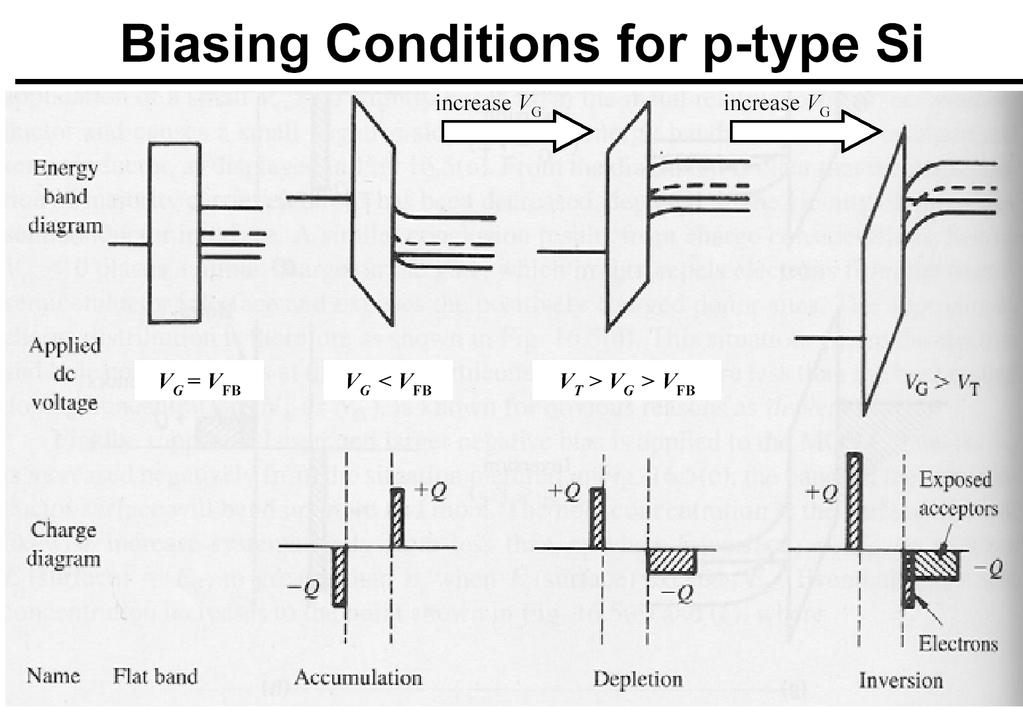
9 MOS Operation Modes A) Accumulation: V G < V FB for p-type substrate M O Si (p-si) holes Thickness of accumulation layer ~0 V Si 0, so V o = V G - V FB Q Si = charge/unit area in Si =C o (V G - V FB ) 9
10 MOS Operation Modes B) Flatband: V G = V FB No charge in Si (and hence no charge in metal gate) V Si = V o = 0 M O S (p-si) 10
11 MOS Operation Modes (cont.) C) Depletion: V G > V FB d = 2εSiV qn B Si M O S (p-si) d qn B V G = V FB + qn C B o d + qn B 2ε s 2 d (can solve for d ) Depletion layer V o V Si 11
12 Depletion Mode :Charge and Electric Field Distributions by Superposition Principle of Electrostatics Metal ρ() Q' Oide Semiconductor = o + d Metal ρ() Q' Oide Semiconductor Metal ρ() Oide Q' Semiconductor = o + d =0 = o ρ =0 - Q' = o =0 = o ρ Metal E() Oide Semiconductor = o + d = Metal E() Oide Semiconductor = o + d + Metal E() Oide Semiconductor = o + d =0 = o =0 = o =0 = o 12
13 MOS Operation Modes (cont.) D) Threshold of Inversion: V G = V T n surface = N B => V Si = 2 Φ F (for p-type substrate) This is a definition for onset of strong inversion M O S (p-si) dma qn B Q n V G 2 ε s ( 2 Φ F ) qn B = V T = V FB C o Φ F 13
14 MOS Operation Modes (cont.) E) Strong Inversion: V G > V T dma is approimately unchanged d ma = 4ε Si qn Φ B F when V G > V T M O S (p-si) dma V Q o n = qn C B o ( V d ma C G o + Q V T ) n Q n qn a electrons 14
15 15
16 16
17 p-si 17
18 Suggested Eercise Most derivations for MOS shown in lecture notes are done with p-type substrate (NMOS) as eample. Repeat the derivations yourself for n-type substrate (PMOS) to test your understanding of MOS. 18
19 p-si substrate (NMOS) Accumulation (holes) V FB depletion V T strong inversion (electrons) V G (more positive) n-si substrate (PMOS) V G (more negative) Strong inversion (holes) V T depletion V FB Accumulation (electrons) 19
20 Voltage drop = area under E-field curve Accumulation V o = Q a /C o V Si ~ 0 V o =qn a d /C o Depletion V Si = qn a d2 /(2ε s ) V o = [qn a dma +Q n ]/C o Inversion V Si = qn a dma2 /(2ε s ) = 2 Φ F * For simplicity, dielectric constants assumed to be same for oide and Si in E-field sketches 20
21 Appendi -Electron Energy Band - Fermi Level -Electrostatics of device charges 21
22 Electron Potential Energy Conduction Band and Valence Band Available states at discreet energy levels Available states as continuous energy levels inside energy bands Isolated atoms Atoms in a solid 22
23 The Simplified Electron Energy Band Diagram 23
24 Energy Band Diagram with E-field Electron Electron Energy - E-field + Energy E-field E C 2 1 E C E V Electric potential φ(2) < φ(1) E V Electric potential φ(2) > φ(1) Electron concentration n n(2) n(1) = e e qφ(2) / kt qφ(1) / kt = e q[ φ(2) φ(1)]/ kt 24
 / kt] where E f is the Fermi energy and k = Boltzmann constant=8.617 10-5 ev/k T=0K f(e) 0.")
25 The Fermi-Dirac Distribution (Fermi Function) Probability of available states at energy E being occupied f(e) = 1/ [ 1+ ep (E- E f ) / kt] where E f is the Fermi energy and k = Boltzmann constant= ev/k T=0K f(e) 0.5 E -E f 25
26 Properties of the Fermi-Dirac Distribution Probability of electron state at energy E will be occupied (1) f(e) ep [- (E- E f ) / kt] for (E- E f ) > 3kT Note: At 300K, kt= 0.026eV This approimation is called Boltzmann approimation (2) Probability of available states at energy E NOT being occupied 1- f(e) = 1/ [ 1+ ep (E f -E) / kt] 26
27 Fermi Energy (E i ) of Intrinsic Semiconductor Ec E g /2 E i E g /2 Ev 27
28 How to find n, p when Na and Nd are known n- p = Nd - Na (1) pn = ni 2 (2) (i) If Nd -Na > 10 ni : n Nd -Na (ii) If Na - Nd > 10 ni : p Na- Nd 28
29 How to find E f when n(or p) is known E c q Φ F E i E f (n-type) E v E f (p-type) n = n i ep [(E f -E i )/kt] Let qφ F E f -E i n = n i ep [qφ F /kt] 29
30 Dependence of Fermi Level with Doping Concentration E i (E C +E V )/2 Middle of energy gap When Si is undoped, E f = E i ; also n =p = n i 30
31 The Fermi Energy at thermal equilibrium At thermal equilibrium ( i.e., no eternal perturbation), The Fermi Energy must be constant for all positions Electron energy Material A Material B Material C Material D E F Position 31
32 Electron Transfer during contact formation System 1 System 2 System 1 System 2 Before contact formation E F1 e E F2 E F1 e E F2 After contact formation System 1 System 2 Net + - Net positive + - negative charge + - charge E F System 1 System E F - + E E 32
33 Applied Bias and Fermi Level Fermi level of the side which has a relatively higher electric potential will have a relatively lower electron energy ( Potential Energy = -q electric potential.) Only difference of the E 's at both sides are important, not the absolute position of the Fermi levels. E f1 qv a E f2 E f1 q V a E f 2 Side 1 Side 2 Side 1 Side V a > 0 V a < 0 Potential difference across depletion region = V bi -V a 33
34 PN junctions Thermal Equilibrium N A- and p ρ() is 0 E-field Depletion region N + D and n ρ() is Quasi-neutral region Quasi-neutral region p-si N A- only ρ() is - n-si N D+ only ρ() is + Complete Depletion Approimation used for charges inside depletion region r() N D+ () N A- () 34
35 Electrostatics of Device Charges 1) Summation of all charges = 0 ρ 2 d2 = ρ 1 d1 2) E-field =0 outside depletion regions p-type ρ() Semiconductor n-type Semiconductor ρ2 - - d1 ρ1 d2 E = 0 =0 E 0 E = 0 35
36 3) Relationship between E-field and charge density ρ() d [ε E()] /d = ρ() Gauss Law 4) Relationship between E-field and potential φ E() = - dφ()/d 36
37 Eample Analysis : n+/ p-si junction ρ() n+ Si Depletion region is very thin and is approimated as +Q' =0 Depletion region p-si d -qna E () E ma =qn a d /ε s 3) Slope = qn a /ε s d 2) E = 0 a thin sheet charge 1) Q = qn a d 4) Area under E-field curve = voltage across depletion region = qn a d2 /2ε s 37
38 Superposition Principle ρ() If ρ 1 () E 1 () and V 1 () ρ 2 () E 2 () and V 2 () then ρ 1 () + ρ 2 () E 1 () + E 2 () and V 1 () + V 2 () - -qn A - p + n +qn D =0 ρ 1 () ρ 2 () Q=+qN A p +qn D - p + -qn A + n Q=-qN A p =0 =0 38
39 ρ 1 () ρ 2 () - p Q=+qN A p +qn D -qn A + n =0 E 1 () Q=-qN A p =0 E 2 () - p + n - Slope = -qn A /ε s =0 + - =0 Slope = +qn D /ε s 39
40 Sketch of E() E() = E 1 ()+ E 2 () - p + n =0 Slope = - qn A /ε s Slope = + qn D /ε s - Ema = - qn A p /ε s = - qn D n /ε s 40
41 δ Why dma ~ constant beyond onset of strong inversion? G Higher than V T δ V = V + V + V n ln FB E i E f ( n ) e δ kt OX Picks up all the changes in V G Si Approimation assumes V Si does not change much Justification: If surface electron density changes by n V OX n C OX but the change of V Si changes only by kt/q [ ln ( n)] small! 41
42 n-surface = n-bulk e qvsi/kt n-surface qv Si p-si N a =10 16 /cm3 n-bulk = /cm3 E i 0.35eV E f Onset of strong inversion (at V T ) VSi n-surface E E E E E E E E E E+19 42
Lecture 04 Review of MOSFET
 ECE 541/ME 541 Microelectronic Fabrication Techniques Lecture 04 Review of MOSFET Zheng Yang (ERF 3017, email: yangzhen@uic.edu) What is a Transistor? A Switch! An MOS Transistor V GS V T V GS S Ron D
Section 12: Intro to Devices
 Section 12: Intro to Devices Extensive reading materials on reserve, including Robert F. Pierret, Semiconductor Device Fundamentals Bond Model of Electrons and Holes Si Si Si Si Si Si Si Si Si Silicon
EE 560 MOS TRANSISTOR THEORY
 1 EE 560 MOS TRANSISTOR THEORY PART 1 TWO TERMINAL MOS STRUCTURE V G (GATE VOLTAGE) 2 GATE OXIDE SiO 2 SUBSTRATE p-type doped Si (N A = 10 15 to 10 16 cm -3 ) t ox V B (SUBSTRATE VOLTAGE) EQUILIBRIUM:
Lecture 12: MOS Capacitors, transistors. Context
 Lecture 12: MOS Capacitors, transistors Context In the last lecture, we discussed PN diodes, and the depletion layer into semiconductor surfaces. Small signal models In this lecture, we will apply those
MOS Capacitor MOSFET Devices. MOSFET s. INEL Solid State Electronics. Manuel Toledo Quiñones. ECE Dept. UPRM.
 INEL 6055 - Solid State Electronics ECE Dept. UPRM 20th March 2006 Definitions MOS Capacitor Isolated Metal, SiO 2, Si Threshold Voltage qφ m metal d vacuum level SiO qχ 2 E g /2 qφ F E C E i E F E v qφ
ESE 570: Digital Integrated Circuits and VLSI Fundamentals
 ESE 570: Digital Integrated Circuits and VLSI Fundamentals Lec 4: January 24, 2017 MOS Transistor Theory, MOS Model Penn ESE 570 Spring 2017 Khanna Lecture Outline! Semiconductor Physics " Band gaps "
ESE 570: Digital Integrated Circuits and VLSI Fundamentals
 ESE 570: Digital Integrated Circuits and VLSI Fundamentals Lec 4: January 23, 2018 MOS Transistor Theory, MOS Model Penn ESE 570 Spring 2018 Khanna Lecture Outline! CMOS Process Enhancements! Semiconductor
Lecture 15 OUTLINE. MOSFET structure & operation (qualitative) Review of electrostatics The (N)MOS capacitor
 Review of electrostatics The (N)MOS capacitor") Lecture 15 OUTLINE MOSFET structure & operation (qualitative) Review of electrostatics The (N)MOS capacitor Electrostatics t ti Charge vs. voltage characteristic Reading: Chapter 6.1 6.2.1 EE105 Fall 2007
Lecture 15 OUTLINE MOSFET structure & operation (qualitative) Review of electrostatics The (N)MOS capacitor Electrostatics t ti Charge vs. voltage characteristic Reading: Chapter 6.1 6.2.1 EE105 Fall 2007
Week 3, Lectures 6-8, Jan 29 Feb 2, 2001
 Week 3, Lectures 6-8, Jan 29 Feb 2, 2001 EECS 105 Microelectronics Devices and Circuits, Spring 2001 Andrew R. Neureuther Topics: M: Charge density, electric field, and potential; W: Capacitance of pn
FIELD-EFFECT TRANSISTORS
 FIEL-EFFECT TRANSISTORS 1 Semiconductor review 2 The MOS capacitor 2 The enhancement-type N-MOS transistor 3 I-V characteristics of enhancement MOSFETS 4 The output characteristic of the MOSFET in saturation
Semiconductor Physics Problems 2015
 Semiconductor Physics Problems 2015 Page and figure numbers refer to Semiconductor Devices Physics and Technology, 3rd edition, by SM Sze and M-K Lee 1. The purest semiconductor crystals it is possible
Lecture 15 OUTLINE. MOSFET structure & operation (qualitative) Review of electrostatics The (N)MOS capacitor
 Review of electrostatics The (N)MOS capacitor") Lecture 15 OUTLINE MOSFET structure & operation (qualitative) Review of electrostatics The (N)MOS capacitor Electrostatics Charge vs. voltage characteristic Reading: Chapter 6.1 6.2.1 EE15 Spring 28 Lecture
Lecture 15 OUTLINE MOSFET structure & operation (qualitative) Review of electrostatics The (N)MOS capacitor Electrostatics Charge vs. voltage characteristic Reading: Chapter 6.1 6.2.1 EE15 Spring 28 Lecture
ESE 570: Digital Integrated Circuits and VLSI Fundamentals
 ESE 570: Digital Integrated Circuits and VLSI Fundamentals Lec 4: January 29, 2019 MOS Transistor Theory, MOS Model Penn ESE 570 Spring 2019 Khanna Lecture Outline! CMOS Process Enhancements! Semiconductor
Lecture 8 PN Junction and MOS Electrostatics (V) Electrostatics of Metal Oxide Semiconductor Structure (cont.) October 4, 2005
 Electrostatics of Metal Oxide Semiconductor Structure (cont.) October 4, 2005") 6.12 Microelectronic Devices and Circuits Fall 25 Lecture 8 1 Lecture 8 PN Junction and MOS Electrostatics (V) Electrostatics of Metal Oide Semiconductor Structure (cont.) Contents: October 4, 25 1. Overview
6.12 Microelectronic Devices and Circuits Fall 25 Lecture 8 1 Lecture 8 PN Junction and MOS Electrostatics (V) Electrostatics of Metal Oide Semiconductor Structure (cont.) Contents: October 4, 25 1. Overview
UNIVERSITY OF CALIFORNIA College of Engineering Department of Electrical Engineering and Computer Sciences. EECS 130 Professor Ali Javey Fall 2006
 UNIVERSITY OF CALIFORNIA College of Engineering Department of Electrical Engineering and Computer Sciences EECS 130 Professor Ali Javey Fall 2006 Midterm 2 Name: SID: Closed book. Two sheets of notes are
Section 12: Intro to Devices
 Section 12: Intro to Devices Extensive reading materials on reserve, including Robert F. Pierret, Semiconductor Device Fundamentals EE143 Ali Javey Bond Model of Electrons and Holes Si Si Si Si Si Si Si
Lecture 17 - p-n Junction. October 11, Ideal p-n junction in equilibrium 2. Ideal p-n junction out of equilibrium
 6.72J/3.43J - Integrated Microelectronic Devices - Fall 22 Lecture 17-1 Lecture 17 - p-n Junction October 11, 22 Contents: 1. Ideal p-n junction in equilibrium 2. Ideal p-n junction out of equilibrium
Lecture 7 - PN Junction and MOS Electrostatics (IV) Electrostatics of Metal-Oxide-Semiconductor Structure. September 29, 2005
 Electrostatics of Metal-Oxide-Semiconductor Structure. September 29, 2005") 6.12 - Microelectronic Devices and Circuits - Fall 25 Lecture 7-1 Lecture 7 - PN Junction and MOS Electrostatics (IV) Electrostatics of Metal-Oide-Semiconductor Structure September 29, 25 Contents: 1.
6.12 - Microelectronic Devices and Circuits - Fall 25 Lecture 7-1 Lecture 7 - PN Junction and MOS Electrostatics (IV) Electrostatics of Metal-Oide-Semiconductor Structure September 29, 25 Contents: 1.
ESE 570 MOS TRANSISTOR THEORY Part 1. Kenneth R. Laker, University of Pennsylvania, updated 5Feb15
 ESE 570 MOS TRANSISTOR THEORY Part 1 TwoTerminal MOS Structure 2 GATE Si Oxide interface n n Mass Action Law VB 2 Chemical Periodic Table Donors American Chemical Society (ACS) Acceptors Metalloids 3 Ideal
Lecture Outline. ESE 570: Digital Integrated Circuits and VLSI Fundamentals. Review: MOSFET N-Type, P-Type. Semiconductor Physics.
 ESE 57: Digital Integrated Circuits and VLSI Fundamentals Lec 4: January 24, 217 MOS Transistor Theory, MOS Model Lecture Outline! Semiconductor Physics " Band gaps " Field Effects! MOS Physics " Cutoff
! CMOS Process Enhancements. ! Semiconductor Physics. " Band gaps. " Field Effects. ! MOS Physics. " Cut-off. " Depletion.
 ESE 570: Digital Integrated Circuits and VLSI Fundamentals Lec 4: January 3, 018 MOS Transistor Theory, MOS Model Lecture Outline! CMOS Process Enhancements! Semiconductor Physics " Band gaps " Field Effects!
Semiconductor Junctions
 8 Semiconductor Junctions Almost all solar cells contain junctions between different materials of different doping. Since these junctions are crucial to the operation of the solar cell, we will discuss
EE105 - Spring 2007 Microelectronic Devices and Circuits. Structure and Symbol of MOSFET. MOS Capacitor. Metal-Oxide-Semiconductor (MOS) Capacitor
 Capacitor") EE105 - Spring 007 Microelectronic Device and ircuit Metal-Oide-Semiconductor (MOS) apacitor Lecture 4 MOS apacitor The MOS tructure can be thought of a a parallel-plate capacitor, with the top plate being
EE105 - Spring 007 Microelectronic Device and ircuit Metal-Oide-Semiconductor (MOS) apacitor Lecture 4 MOS apacitor The MOS tructure can be thought of a a parallel-plate capacitor, with the top plate being
Lecture 7 PN Junction and MOS Electrostatics(IV) Metal Oxide Semiconductor Structure (contd.)
 Metal Oxide Semiconductor Structure (contd.)") Lecture 7 PN Junction and MOS Electrostatics(IV) Metal Oxide Semiconductor Structure (contd.) Outline 1. Overview of MOS electrostatics under bias 2. Depletion regime 3. Flatband 4. Accumulation regime
Lecture 7 PN Junction and MOS Electrostatics(IV) Metal Oxide Semiconductor Structure (contd.) Outline 1. Overview of MOS electrostatics under bias 2. Depletion regime 3. Flatband 4. Accumulation regime
! CMOS Process Enhancements. ! Semiconductor Physics. " Band gaps. " Field Effects. ! MOS Physics. " Cut-off. " Depletion.
 ESE 570: Digital Integrated Circuits and VLSI Fundamentals Lec 4: January 9, 019 MOS Transistor Theory, MOS Model Lecture Outline CMOS Process Enhancements Semiconductor Physics Band gaps Field Effects
ECE-305: Fall 2017 Metal Oxide Semiconductor Devices
 C-305: Fall 2017 Metal Oxide Semiconductor Devices Pierret, Semiconductor Device Fundamentals (SDF) Chapters 15+16 (pp. 525-530, 563-599) Professor Peter Bermel lectrical and Computer ngineering Purdue
SECTION: Circle one: Alam Lundstrom. ECE 305 Exam 5 SOLUTIONS: Spring 2016 April 18, 2016 M. A. Alam and M.S. Lundstrom Purdue University
 NAME: PUID: SECTION: Circle one: Alam Lundstrom ECE 305 Exam 5 SOLUTIONS: April 18, 2016 M A Alam and MS Lundstrom Purdue University This is a closed book exam You may use a calculator and the formula
Semiconductor Devices. C. Hu: Modern Semiconductor Devices for Integrated Circuits Chapter 5
 Semiconductor Devices C. Hu: Modern Semiconductor Devices for Integrated Circuits Chapter 5 Global leader in environmental and industrial measurement Wednesday 3.2. afternoon Tour around facilities & lecture
ECE 340 Lecture 39 : MOS Capacitor II
 ECE 340 Lecture 39 : MOS Capacitor II Class Outline: Effects of Real Surfaces Threshold Voltage MOS Capacitance-Voltage Analysis Things you should know when you leave Key Questions What are the effects
MOS CAPACITOR AND MOSFET
 EE336 Semiconductor Devices 1 MOS CAPACITOR AND MOSFET Dr. Mohammed M. Farag Ideal MOS Capacitor Semiconductor Devices Physics and Technology Chapter 5 EE336 Semiconductor Devices 2 MOS Capacitor Structure
Final Examination EE 130 December 16, 1997 Time allotted: 180 minutes
 Final Examination EE 130 December 16, 1997 Time allotted: 180 minutes Problem 1: Semiconductor Fundamentals [30 points] A uniformly doped silicon sample of length 100µm and cross-sectional area 100µm 2
Microelectronic Devices and Circuits Lecture 9 - MOS Capacitors I - Outline Announcements Problem set 5 -
 6.012 - Microelectronic Devices and Circuits Lecture 9 - MOS Capacitors I - Outline Announcements Problem set 5 - Posted on Stellar. Due net Wednesday. Qualitative description - MOS in thermal equilibrium
The Intrinsic Silicon
 The Intrinsic ilicon Thermally generated electrons and holes Carrier concentration p i =n i ni=1.45x10 10 cm-3 @ room temp Generally: n i = 3.1X10 16 T 3/2 e -1.21/2KT cm -3 T= temperature in K o (egrees
Lecture 22 Field-Effect Devices: The MOS Capacitor
 Lecture 22 Field-Effect Devices: The MOS Capacitor F. Cerrina Electrical and Computer Engineering University of Wisconsin Madison Click here for link to F.C. homepage Spring 1999 0 Madison, 1999-II Topics
an introduction to Semiconductor Devices
 an introduction to Semiconductor Devices Donald A. Neamen Chapter 6 Fundamentals of the Metal-Oxide-Semiconductor Field-Effect Transistor Introduction: Chapter 6 1. MOSFET Structure 2. MOS Capacitor -
Lecture 11: MOS Transistor
 Lecture 11: MOS Transistor Prof. Niknejad Lecture Outline Review: MOS Capacitors Regions MOS Capacitors (3.8 3.9) CV Curve Threshold Voltage MOS Transistors (4.1 4.3): Overview Cross-section and layout
Semiconductor Physics fall 2012 problems
 Semiconductor Physics fall 2012 problems 1. An n-type sample of silicon has a uniform density N D = 10 16 atoms cm -3 of arsenic, and a p-type silicon sample has N A = 10 15 atoms cm -3 of boron. For each
ECE 305 Exam 5 SOLUTIONS: Spring 2015 April 17, 2015 Mark Lundstrom Purdue University
 NAME: PUID: : ECE 305 Exam 5 SOLUTIONS: April 17, 2015 Mark Lundstrom Purdue University This is a closed book exam. You may use a calculator and the formula sheet at the end of this exam. Following the
Lecture 6 PN Junction and MOS Electrostatics(III) Metal-Oxide-Semiconductor Structure
 Metal-Oxide-Semiconductor Structure") Lecture 6 PN Junction and MOS Electrostatics(III) Metal-Oxide-Semiconductor Structure Outline 1. Introduction to MOS structure 2. Electrostatics of MOS in thermal equilibrium 3. Electrostatics of MOS with
Lecture 6 PN Junction and MOS Electrostatics(III) Metal-Oxide-Semiconductor Structure Outline 1. Introduction to MOS structure 2. Electrostatics of MOS in thermal equilibrium 3. Electrostatics of MOS with
EE 130 Intro to MS Junctions Week 6 Notes. What is the work function? Energy to excite electron from Fermi level to the vacuum level
 EE 13 Intro to S Junctions eek 6 Notes Problem 1 hat is the work function? Energy to ecite electron from Fermi level to the vacuum level Electron affinity of 4.5eV Electron affinity of Ge 4.eV orkfunction
Extensive reading materials on reserve, including
 Section 12: Intro to Devices Extensive reading materials on reserve, including Robert F. Pierret, Semiconductor Device Fundamentals EE143 Ali Javey Bond Model of Electrons and Holes Si Si Si Si Si Si Si
ECEN 3320 Semiconductor Devices Final exam - Sunday December 17, 2000
 Your Name: ECEN 3320 Semiconductor Devices Final exam - Sunday December 17, 2000 1. Review questions a) Illustrate the generation of a photocurrent in a p-n diode by drawing an energy band diagram. Indicate
Classification of Solids
 Classification of Solids Classification by conductivity, which is related to the band structure: (Filled bands are shown dark; D(E) = Density of states) Class Electron Density Density of States D(E) Examples
EECS130 Integrated Circuit Devices
 EECS130 Integrated Circuit Devices Professor Ali Javey 10/02/2007 MS Junctions, Lecture 2 MOS Cap, Lecture 1 Reading: finish chapter14, start chapter16 Announcements Professor Javey will hold his OH at
Class 05: Device Physics II
 Topics: 1. Introduction 2. NFET Model and Cross Section with Parasitics 3. NFET as a Capacitor 4. Capacitance vs. Voltage Curves 5. NFET as a Capacitor - Band Diagrams at V=0 6. NFET as a Capacitor - Accumulation
Chapter 7. The pn Junction
 Chapter 7 The pn Junction Chapter 7 PN Junction PN junction can be fabricated by implanting or diffusing donors into a P-type substrate such that a layer of semiconductor is converted into N type. Converting
Quiz #1 Practice Problem Set
 Name: Student Number: ELEC 3908 Physical Electronics Quiz #1 Practice Problem Set? Minutes January 22, 2016 - No aids except a non-programmable calculator - All questions must be answered - All questions
Department of Electrical and Computer Engineering, Cornell University. ECE 3150: Microelectronics. Spring Due on March 01, 2018 at 7:00 PM
 Department of Electrical and Computer Engineering, Cornell University ECE 3150: Microelectronics Spring 2018 Homework 4 Due on March 01, 2018 at 7:00 PM Suggested Readings: a) Lecture notes Important Note:
Fundamentals of the Metal Oxide Semiconductor Field-Effect Transistor
 Triode Working FET Fundamentals of the Metal Oxide Semiconductor Field-Effect Transistor The characteristics of energy bands as a function of applied voltage. Surface inversion. The expression for the
UNIVERSITY OF CALIFORNIA College of Engineering Department of Electrical Engineering and Computer Sciences. EECS 130 Professor Ali Javey Fall 2006
 UNIVERSITY OF CALIFORNIA College of Engineering Department of Electrical Engineering and Computer Sciences EECS 130 Professor Ali Javey Fall 2006 Midterm I Name: Closed book. One sheet of notes is allowed.
Choice of V t and Gate Doping Type
 Choice of V t and Gate Doping Type To make circuit design easier, it is routine to set V t at a small positive value, e.g., 0.4 V, so that, at V g = 0, the transistor does not have an inversion layer and
EE105 - Fall 2006 Microelectronic Devices and Circuits
 EE105 - Fall 2006 Microelectronic Devices and Circuits Prof. Jan M. Rabaey (jan@eecs) Lecture 7: MOS Transistor Some Administrative Issues Lab 2 this week Hw 2 due on We Hw 3 will be posted same day MIDTERM
Lecture 4 - PN Junction and MOS Electrostatics (I) Semiconductor Electrostatics in Thermal Equilibrium September 20, 2005
 Semiconductor Electrostatics in Thermal Equilibrium September 20, 2005") 6.012 - Microelectronic Devices and Circuits - Fall 2005 Lecture 4-1 Contents: Lecture 4 - PN Junction and MOS Electrostatics (I) Semiconductor Electrostatics in Thermal Equilibrium September 20, 2005
6.012 - Microelectronic Devices and Circuits - Fall 2005 Lecture 4-1 Contents: Lecture 4 - PN Junction and MOS Electrostatics (I) Semiconductor Electrostatics in Thermal Equilibrium September 20, 2005
Midterm I - Solutions
 UNIVERSITY OF CALIFORNIA College of Engineering Department of Electrical Engineering and Computer Sciences EECS 130 Spring 2008 Professor Chenming Hu Midterm I - Solutions Name: SID: Grad/Undergrad: Closed
ECE 342 Electronic Circuits. Lecture 6 MOS Transistors
 ECE 342 Electronic Circuits Lecture 6 MOS Transistors Jose E. Schutt-Aine Electrical & Computer Engineering University of Illinois jesa@illinois.edu 1 NMOS Transistor Typically L = 0.1 to 3 m, W = 0.2
For the following statements, mark ( ) for true statement and (X) for wrong statement and correct it.
 for true statement and (X) for wrong statement and correct it.") Benha University Faculty of Engineering Shoubra Electrical Engineering Department First Year communications. Answer all the following questions Illustrate your answers with sketches when necessary. The
Benha University Faculty of Engineering Shoubra Electrical Engineering Department First Year communications. Answer all the following questions Illustrate your answers with sketches when necessary. The
n N D n p = n i p N A
 Summary of electron and hole concentration in semiconductors Intrinsic semiconductor: E G n kt i = pi = N e 2 0 Donor-doped semiconductor: n N D where N D is the concentration of donor impurity Acceptor-doped
Operation and Modeling of. The MOS Transistor. Second Edition. Yannis Tsividis Columbia University. New York Oxford OXFORD UNIVERSITY PRESS
 Operation and Modeling of The MOS Transistor Second Edition Yannis Tsividis Columbia University New York Oxford OXFORD UNIVERSITY PRESS CONTENTS Chapter 1 l.l 1.2 1.3 1.4 1.5 1.6 1.7 Chapter 2 2.1 2.2
Consider a uniformly doped PN junction, in which one region of the semiconductor is uniformly doped with acceptor atoms and the adjacent region is
 CHAPTER 7 The PN Junction Consider a uniformly doped PN junction, in which one region of the semiconductor is uniformly doped with acceptor atoms and the adjacent region is uniformly doped with donor atoms.
Integrated Circuits & Systems
 Federal University of Santa Catarina Center for Technology Computer Science & Electronics Engineering Integrated Circuits & Systems INE 5442 Lecture 10 MOSFET part 1 guntzel@inf.ufsc.br ual-well Trench-Isolated
Session 6: Solid State Physics. Diode
 Session 6: Solid State Physics Diode 1 Outline A B C D E F G H I J 2 Definitions / Assumptions Homojunction: the junction is between two regions of the same material Heterojunction: the junction is between
Dept. of Materials Science and Engineering. Electrical Properties Of Materials
 Problem Set 12 Solutions See handout "Part 4: Heterojunctions MOS Devices" (slides 9-18) Using the Boise State Energy Band Diagram program, build the following structure: Gate material: 5nm p + -Poly Si
6.012 Electronic Devices and Circuits
 Page 1 of 12 YOUR NAME Department of Electrical Engineering and Computer Science Massachusetts Institute of Technology 6.012 Electronic Devices and Circuits FINAL EXAMINATION Open book. Notes: 1. Unless
MENA9510 characterization course: Capacitance-voltage (CV) measurements
 measurements") MENA9510 characterization course: Capacitance-voltage (CV) measurements 30.10.2017 Halvard Haug Outline Overview of interesting sample structures Ohmic and schottky contacts Why C-V for solar cells? The
MENA9510 characterization course: Capacitance-voltage (CV) measurements 30.10.2017 Halvard Haug Outline Overview of interesting sample structures Ohmic and schottky contacts Why C-V for solar cells? The
CMPEN 411 VLSI Digital Circuits. Lecture 03: MOS Transistor
 CMPEN 411 VLSI Digital Circuits Lecture 03: MOS Transistor Kyusun Choi [Adapted from Rabaey s Digital Integrated Circuits, Second Edition, 2003 J. Rabaey, A. Chandrakasan, B. Nikolic] CMPEN 411 L03 S.1
ECE606: Solid State Devices Lecture 24 MOSFET non-idealities
 EE66: Solid State Devices Lecture 24 MOSFET non-idealities Gerhard Klimeck gekco@purdue.edu Outline ) Flat band voltage - What is it and how to measure it? 2) Threshold voltage shift due to trapped charges
The Devices: MOS Transistors
 The Devices: MOS Transistors References: Semiconductor Device Fundamentals, R. F. Pierret, Addison-Wesley Digital Integrated Circuits: A Design Perspective, J. Rabaey et.al. Prentice Hall NMOS Transistor
Part 4: Heterojunctions - MOS Devices. MOSFET Current Voltage Characteristics
 MOS Device Uses: Part 4: Heterojunctions - MOS Devices MOSCAP capacitor: storing charge, charge-coupled device (CCD), etc. MOSFET transistor: switch, current amplifier, dynamic random access memory (DRAM-volatile),
Lecture 22 - The Si surface and the Metal-Oxide-Semiconductor Structure (cont.) April 2, 2007
 April 2, 2007") 6.720J/3.43J - Integrated Microelectronic Devices - Spring 2007 Lecture 22-1 Lecture 22 - The Si surface and the Metal-Oxide-Semiconductor Structure (cont.) April 2, 2007 Contents: 1. Ideal MOS structure
6.720J/3.43J - Integrated Microelectronic Devices - Spring 2007 Lecture 22-1 Lecture 22 - The Si surface and the Metal-Oxide-Semiconductor Structure (cont.) April 2, 2007 Contents: 1. Ideal MOS structure
Schottky Rectifiers Zheng Yang (ERF 3017,
 ECE442 Power Semiconductor Devices and Integrated Circuits Schottky Rectifiers Zheng Yang (ERF 3017, email: yangzhen@uic.edu) Power Schottky Rectifier Structure 2 Metal-Semiconductor Contact The work function
Semiconductor Physics fall 2012 problems
 Semiconductor Physics fall 2012 problems 1. An n-type sample of silicon has a uniform density N D = 10 16 atoms cm -3 of arsenic, and a p-type silicon sample has N A = 10 15 atoms cm -3 of boron. For each
MOSFET: Introduction
 E&CE 437 Integrated VLSI Systems MOS Transistor 1 of 30 MOSFET: Introduction Metal oxide semiconductor field effect transistor (MOSFET) or MOS is widely used for implementing digital designs Its major
1 Name: Student number: DEPARTMENT OF PHYSICS AND PHYSICAL OCEANOGRAPHY MEMORIAL UNIVERSITY OF NEWFOUNDLAND. Fall :00-11:00
 1 Name: DEPARTMENT OF PHYSICS AND PHYSICAL OCEANOGRAPHY MEMORIAL UNIVERSITY OF NEWFOUNDLAND Final Exam Physics 3000 December 11, 2012 Fall 2012 9:00-11:00 INSTRUCTIONS: 1. Answer all seven (7) questions.
Sample Exam # 2 ECEN 3320 Fall 2013 Semiconductor Devices October 28, 2013 Due November 4, 2013
 Sample Exam # 2 ECEN 3320 Fall 203 Semiconductor Devices October 28, 203 Due November 4, 203. Below is the capacitance-voltage curve measured from a Schottky contact made on GaAs at T 300 K. Figure : Capacitance
Appendix 1: List of symbols
 Appendix 1: List of symbols Symbol Description MKS Units a Acceleration m/s 2 a 0 Bohr radius m A Area m 2 A* Richardson constant m/s A C Collector area m 2 A E Emitter area m 2 b Bimolecular recombination
UNIVERSITY OF CALIFORNIA, BERKELEY College of Engineering Department of Electrical Engineering and Computer Sciences
 UNIVERSITY OF CALIFORNIA, BERKELEY College of Engineering Department of Electrical Engineering and Computer Sciences EE 105: Microelectronic Devices and Circuits Spring 2008 MIDTERM EXAMINATION #1 Time
Semiconductor Integrated Process Design (MS 635)
") Semiconductor Integrated Process Design (MS 635) Instructor: Prof. Keon Jae Lee - Office: 응용공학동 #4306, Tel: #3343 - Email: keonlee@kaist.ac.kr Lecture: (Tu, Th), 1:00-2:15 #2425 Office hour: Tues & Thur
Semiconductor Integrated Process Design (MS 635) Instructor: Prof. Keon Jae Lee - Office: 응용공학동 #4306, Tel: #3343 - Email: keonlee@kaist.ac.kr Lecture: (Tu, Th), 1:00-2:15 #2425 Office hour: Tues & Thur
Content. MIS Capacitor. Accumulation Depletion Inversion MOS CAPACITOR. A Cantoni Digital Switching
 Content MIS Capacitor Accumulation Depletion Inversion MOS CAPACITOR 1 MIS Capacitor Metal Oxide C ox p-si C s Components of a capacitance model for the MIS structure 2 MIS Capacitor- Accumulation ρ( x)
UNIVERSITY OF CALIFORNIA College of Engineering Department of Electrical Engineering and Computer Sciences. Professor Chenming Hu.
 UNIVERSITY OF CALIFORNIA College of Engineering Department of Electrical Engineering and Computer Sciences EECS 130 Spring 2009 Professor Chenming Hu Midterm I Name: Closed book. One sheet of notes is
Electrical Characteristics of Multilayer MoS 2 FET s
 Electrical Characteristics of Multilayer MoS 2 FET s with MoS 2 /Graphene Hetero-Junction Contacts Joon Young Kwak,* Jeonghyun Hwang, Brian Calderon, Hussain Alsalman, Nini Munoz, Brian Schutter, and Michael
Lecture 4 - PN Junction and MOS Electrostatics (I) Semiconductor Electrostatics in Thermal Equilibrium. February 13, 2003
 Semiconductor Electrostatics in Thermal Equilibrium. February 13, 2003") 6.012 - Microelectronic Devices and Circuits - Spring 2003 Lecture 4-1 Contents: Lecture 4 - PN Junction and MOS Electrostatics (I) Semiconductor Electrostatics in Thermal Equilibrium February 13, 2003
6.012 - Microelectronic Devices and Circuits - Spring 2003 Lecture 4-1 Contents: Lecture 4 - PN Junction and MOS Electrostatics (I) Semiconductor Electrostatics in Thermal Equilibrium February 13, 2003
Lecture 13 - Carrier Flow (cont.), Metal-Semiconductor Junction. October 2, 2002
, Metal-Semiconductor Junction. October 2, 2002") 6.72J/3.43J - Integrated Microelectronic Devices - Fall 22 Lecture 13-1 Contents: Lecture 13 - Carrier Flow (cont.), Metal-Semiconductor Junction October 2, 22 1. Transport in space-charge and high-resistivity
6.72J/3.43J - Integrated Microelectronic Devices - Fall 22 Lecture 13-1 Contents: Lecture 13 - Carrier Flow (cont.), Metal-Semiconductor Junction October 2, 22 1. Transport in space-charge and high-resistivity
Long Channel MOS Transistors
 Long Channel MOS Transistors The theory developed for MOS capacitor (HO #2) can be directly extended to Metal-Oxide-Semiconductor Field-Effect transistors (MOSFET) by considering the following structure:
MSE 310/ECE 340: Electrical Properties of Materials Fall 2014 Department of Materials Science and Engineering Boise State University
 MSE 310/ECE 340: Electrical Properties of Materials Fall 2014 Department of Materials Science and Engineering Boise State University Practice Final Exam 1 Read the questions carefully Label all figures
Junction Diodes. Tim Sumner, Imperial College, Rm: 1009, x /18/2006
 Junction Diodes Most elementary solid state junction electronic devices. They conduct in one direction (almost correct). Useful when one converts from AC to DC (rectifier). But today diodes have a wide
The Three terminal MOS structure. Semiconductor Devices: Operation and Modeling 115
 The Three terminal MOS structure 115 Introduction MOS transistor two terminal MOS with another two opposite terminal (back to back of inversion layer). Theses two new terminal make the current flow if
ECE321 Electronics I
 ECE321 Electronics I Lecture 4: Physics of Semiconductor iodes Payman Zarkesh-Ha Office: ECE Bldg. 230B Office hours: Tuesday 2:00-3:00PM or by appointment E-mail: pzarkesh.unm.edu Slide: 1 Review of Last
Thermionic Emission Theory
 hapter 4. PN and Metal-Semiconductor Junction Thermionic Emiion Theory Energy band diagram of a Schottky contact with a forward bia V applied between the metal and the emiconductor. Electron concentration
Lecture 7 MOS Capacitor
 EE 471: Transport Phenomena in Solid State Devices Spring 2018 Lecture 7 MOS Capacitor Bryan Ackland Department of Electrical and Computer Engineering Stevens Institute of Technology Hoboken, NJ 07030
Lecture 15: MOS Transistor models: Body effects, SPICE models. Context. In the last lecture, we discussed the modes of operation of a MOS FET:
 Lecture 15: MOS Transistor models: Body effects, SPICE models Context In the last lecture, we discussed the modes of operation of a MOS FET: oltage controlled resistor model I- curve (Square-Law Model)
Lecture 12: MOSFET Devices
 Lecture 12: MOSFET Devices Gu-Yeon Wei Division of Engineering and Applied Sciences Harvard University guyeon@eecs.harvard.edu Wei 1 Overview Reading S&S: Chapter 5.1~5.4 Supplemental Reading Background
Device Models (PN Diode, MOSFET )
") Device Models (PN Diode, MOSFET ) Instructor: Steven P. Levitan steve@ece.pitt.edu TA: Gayatri Mehta, José Martínez Book: Digital Integrated Circuits: A Design Perspective; Jan Rabaey Lab Notes: Handed
Device Models (PN Diode, MOSFET ) Instructor: Steven P. Levitan steve@ece.pitt.edu TA: Gayatri Mehta, José Martínez Book: Digital Integrated Circuits: A Design Perspective; Jan Rabaey Lab Notes: Handed
1. The MOS Transistor. Electrical Conduction in Solids
 Electrical Conduction in Solids!The band diagram describes the energy levels for electron in solids.!the lower filled band is named Valence Band.!The upper vacant band is named conduction band.!the distance
The Devices. Digital Integrated Circuits A Design Perspective. Jan M. Rabaey Anantha Chandrakasan Borivoje Nikolic. July 30, 2002
 igital Integrated Circuits A esign Perspective Jan M. Rabaey Anantha Chandrakasan Borivoje Nikolic The evices July 30, 2002 Goal of this chapter Present intuitive understanding of device operation Introduction
CHAPTER 5 MOS FIELD-EFFECT TRANSISTORS
 CHAPTER 5 MOS FIELD-EFFECT TRANSISTORS 5.1 The MOS capacitor 5.2 The enhancement-type N-MOS transistor 5.3 I-V characteristics of enhancement mode MOSFETS 5.4 The PMOS transistor and CMOS technology 5.5
ECE 342 Electronic Circuits. 3. MOS Transistors
 ECE 342 Electronic Circuits 3. MOS Transistors Jose E. Schutt-Aine Electrical & Computer Engineering University of Illinois jschutt@emlab.uiuc.edu 1 NMOS Transistor Typically L = 0.1 to 3 m, W = 0.2 to
EECS130 Integrated Circuit Devices
 EECS130 Integrated Circuit Devices Professor Ali Javey 8/30/2007 Semiconductor Fundamentals Lecture 2 Read: Chapters 1 and 2 Last Lecture: Energy Band Diagram Conduction band E c E g Band gap E v Valence
ECE606: Solid State Devices Lecture 23 MOSFET I-V Characteristics MOSFET non-idealities
 ECE66: Solid State evices Lecture 3 MOSFET I- Characteristics MOSFET non-idealities Gerhard Klimeck gekco@purdue.edu Outline 1) Square law/ simplified bulk charge theory ) elocity saturation in simplified
MOS Transistor Theory MOSFET Symbols Current Characteristics of MOSFET. MOS Symbols and Characteristics. nmos Enhancement Transistor
 MOS Transistor Theory MOSFET Symbols Current Characteristics of MOSFET Calculation of t and Important 2 nd Order Effects SmallSignal Signal MOSFET Model Summary Material from: CMOS LSI Design By Weste
Lecture 2. Introduction to semiconductors Structures and characteristics in semiconductors
 Lecture 2 Introduction to semiconductors Structures and characteristics in semiconductors Semiconductor p-n junction Metal Oxide Silicon structure Semiconductor contact Literature Glen F. Knoll, Radiation