ECE 497 JS Lecture - 12 Device Technologies
|
|
|
- Marsha Leonard
- 5 years ago
- Views:
Transcription
1 ECE 497 JS Lecture - 12 Device Technologies Spring 2004 Jose E. Schutt-Aine Electrical & Computer Engineering University of Illinois jose@emlab.uiuc.edu 1
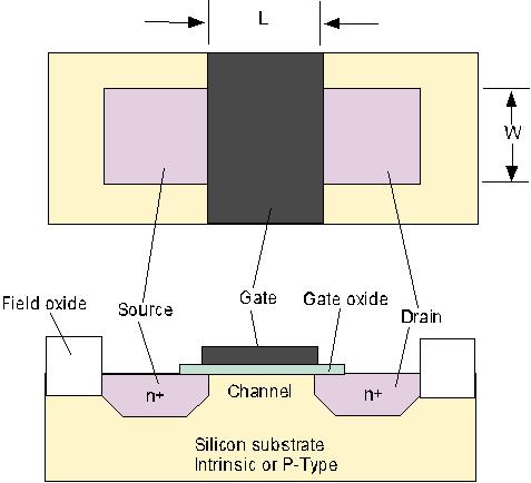
2 NMOS Transistor 2
3 ρ Source channel charge density MOS Regions of Operation inversion layer y Electric field Drain Resistive Region V GT > 0, V small DS ρ channel charge density y Electric field Nonlinear Region Source L Drain V > 0, V = V GT DS GT ρ channel charge density y Saturation Region Source depletion region L- d d Drain V > 0, V V GT DS GT 3
4 Capacitance Gate Capacitance C G determines the amount of charge to switch gate Several distributed components Large discontinuity as device turns on At saturation capacitance is entirely between gate and source 2 1 X Cgs = Cgso + WLCox X Cgd = Cgdo + WLCox X 2 4
5 Gate Capacitance n+ source gate p- C GDO n+ drain n+ source V < 0 V > 0, V small GT GT gate p- DS C GDO n+ drain gate C GDO n+ source n+ drain V GT > p- 0, V large DS 5
6 MOS Regions of Operation Resistive Region For small VDS, FET is a linear resistor Nonlinear Region Charge distribution nonuniform across channel Less charge induced in proximity of drain Saturation Region Channel is pinched off Increase in VDS has little effect Square-law behavior (wrt VGT) Acts like a current source 6
7 MOS Current-Voltage Equations Resistive Region W I = µ C V V L DS n ox GT DS for VDS << V GT I V = β V V 2 DS n GT DS 2 DS for VDS < V GT Saturation Region I DS = V βn 2 2 GT for VDS V GT
8 Current-Voltage Characteristics Threshold voltage Depends on equilibrium potential Controlled by inversion in channel Body Effect V T varies with bias between source and body Leads to modulation of V T 8
9 Body Effect Potential on substrate affects threshold voltage V ( V ) = V + γ (2 φ + V ) (2 φ ) 1/2 1/2 T SB T0 F SB F φ F kt B N a = ln q ni Fermi potential of material γ = ( qn ) 1/2 2 a C ox Body bias coefficient 9
10 NMOS IV Curves 700 NMOS 600 VGS=1.0 VGS=1.5 VGS=2.0 VGS= IDS Vds 10
11 nmos Devices Enhancement Mode Normally off & requires positive potential on gate Good at passing low voltages Cannot pass full V DD (pinch off) Depletion Mode Normally on (negative threshold voltage) Channel is implanted with positive ions ( V T ) Provides inverter with full output swings 11
12 N a N d V Tn V Tp λ γ Saturation velocity m/s µ n Electron mobility 400 cm2 /Vs µ p Hole mobility 100 cm2 /Vs V sat V1/2 k n k p C ox C GSO,C GDO C J C JSW R poly R diff Density of acceptor ions in NFET channel Density of donor ions in PFET channel NFET threshold voltage 0.5 V PFET threshold voltage -0.5 V Channel modulation parameter 0.1 Body effect parameter MOS SPICE Parameters Symbol Description Value Units L drawn Device length (drawn) 0.35 µm L eff Device length (effective) 0.25 µm t ox Gate oxide thickness 70 A NFET process transconductance 200 µa/v2 PFET process transconductance 50 µa/v2 Gate oxide capacitance per unit area 5 ff/µm2 Gate source and drain overlap capacitance 0.1 ff/µm Junction capacitance 0.5 ff/µm2 Junction sidewall capacitance 0.2 ff/µm Gate sheet resistance 4 Ω/square Source and drain sheet resistance 4 Ω/square 0.3 cm-3 cm-3 V -1 12
13 MOS Parasitics Gate R G C GS C GD C GB Source R S Drain C SB C DB Body - Capacitance from gate to other 3 terminals - Diodes to body - Series resistance - Wiring parasitics 13
14 PMOS IV Curves 0 PMOS VGS= VGS=-1.0 VGS=-1.5 VGS=-2.0 VGS= Vds 14
15 PMOS Transistor 0 PMOS Field oxide Source Gate Gate oxide Drain p+ Channel p+ n+ VGS= Well p VGS=-1.0 VGS=-1.5 VGS=-2.0 VGS= Vds - All polarities are reversed from nmos - Hole mobility is lower low transconductance - nmos favored over pmos 15
16 Complementary MOS GND in V DD out in out n+ p- n+ p- p+ p+ n+ 16
17 CMOS Advantages Virtually, no DC power consumed No DC path between power and ground Excellent noise margins (V OL =0, V OH =V DD ) Inverter has sharp transfer curve Drawbacks Requires more transistors Process is more complicated pmos size larger to achieve electrical symmetry Latch up 17
18 Source Coupled Pair V = V1 V2 I = I1 I2 V C V + V 1 2 = 1 2 S I 2 C = = V 2 2 CT β CT I ( ) 1 = β V + = V + V V + V /4 CT 2 2 V 2 2 I2 = β VCT = β V V /4 CT CT V + V 2 I + I ( ) 2β CT I = V V I 18
19 Power Dissipation in Static CMOS Gate Switching energy dissipated in 0-1 transition VDD VDD 2 CVDD sw = ( DD C ) = ( DD C ) C = E V V Idt V V CdV Power dissipation P = E f = CV f 2 sig cy sig DD sig R P In terms of duty factor C P = CV f = CV K f 2 2 DD tog DD D ck R n 19

20 Bipolar Junction Transistor 20
21 BJT Operating Principle E B C n b (0) P co n b P eo n bo n b (W) 0 W b I C = qad b n (0) n ( W ) W ' ' b b b b q: electron charge A: Effective area of E-B junction D b : diffusion constant of electrons in base 21
22 CMOS vs Bipolar Current Collector current inversely proportional to Wb Drain current inversely proportional to L Topology Base width is vertical defined by lithography Channel length is horizontal defined by diffusion Behavior Bipolar current is exponential MOS current obeys square law 22
23 BJT vs MOS Matching V BEon for bipolar is determined by bandgap V T on MOS is determined by t ox and implant BJTs have superior current drive BJTs switch faster than MOS BJTs dissipate more power BJTs have lower yield BJTs are more costly 23
24 Gallium Arsenide Transistors Speed High electron mobility Saturation velocity is reached at lower power Substrate Larger bandgap than Si semi insulating SOI, Lower parasitics Optical Properties Direct bandgap LED, lasers Integrate digital and optics on same IC 24
25 GaAs Limitations Physics Low hole mobility Low thermal conductivity More defects and more fragile Process No oxide more complex process Lower level of integration Cost More expensive Less mature technology 25
26 RF Front End Technologies Product PA LNA Mixer VCO Filter Switch Technology Today GaAs Si SiGe Si Si Si GaAs Si Si GaAs Technology Future Criterion InP GaAs SiGe PAE, linearity InP GaAs Low power InP GaAs Linearity, 1/f noise InP GaAs MEMS 1/f noise High Q InP GaAs MEMS Isolation, Insertion loss 26
27 Device Technologies for RF Applications Si Bipolar GaAs MESFET GaAs HBT InP HBT base resistance high - low low transit time high? low low beta-early voltage product low? high high col-subst capacitance high - low low linearity of DC current gain high? low medium turn on voltage thermal conductivity high? low medium transconductance 50X 1 50X? device matching < 1 mv > 10 mv 1 mv? hysteresis or backgating negligible > 10 mv negligible? device scaling high low medium breakdown voltage < 10 V > 8 V > 10 V low ft (GHz)??? 160 Max resolution (bits) 8 5 8? 27
ECE 342 Electronic Circuits. 3. MOS Transistors
 ECE 342 Electronic Circuits 3. MOS Transistors Jose E. Schutt-Aine Electrical & Computer Engineering University of Illinois jschutt@emlab.uiuc.edu 1 NMOS Transistor Typically L = 0.1 to 3 m, W = 0.2 to
ECE 546 Lecture 10 MOS Transistors
 ECE 546 Lecture 10 MOS Transistors Spring 2018 Jose E. Schutt-Aine Electrical & Computer Engineering University of Illinois jesa@illinois.edu NMOS Transistor NMOS Transistor N-Channel MOSFET Built on p-type
ECE 342 Electronic Circuits. Lecture 6 MOS Transistors
 ECE 342 Electronic Circuits Lecture 6 MOS Transistors Jose E. Schutt-Aine Electrical & Computer Engineering University of Illinois jesa@illinois.edu 1 NMOS Transistor Typically L = 0.1 to 3 m, W = 0.2
MOSFET: Introduction
 E&CE 437 Integrated VLSI Systems MOS Transistor 1 of 30 MOSFET: Introduction Metal oxide semiconductor field effect transistor (MOSFET) or MOS is widely used for implementing digital designs Its major
The Devices. Digital Integrated Circuits A Design Perspective. Jan M. Rabaey Anantha Chandrakasan Borivoje Nikolic. July 30, 2002
 Digital Integrated Circuits A Design Perspective Jan M. Rabaey Anantha Chandrakasan Borivoje Nikolic The Devices July 30, 2002 Goal of this chapter Present intuitive understanding of device operation Introduction
Device Models (PN Diode, MOSFET )
") Device Models (PN Diode, MOSFET ) Instructor: Steven P. Levitan steve@ece.pitt.edu TA: Gayatri Mehta, José Martínez Book: Digital Integrated Circuits: A Design Perspective; Jan Rabaey Lab Notes: Handed
Device Models (PN Diode, MOSFET ) Instructor: Steven P. Levitan steve@ece.pitt.edu TA: Gayatri Mehta, José Martínez Book: Digital Integrated Circuits: A Design Perspective; Jan Rabaey Lab Notes: Handed
CMPEN 411 VLSI Digital Circuits. Lecture 03: MOS Transistor
 CMPEN 411 VLSI Digital Circuits Lecture 03: MOS Transistor Kyusun Choi [Adapted from Rabaey s Digital Integrated Circuits, Second Edition, 2003 J. Rabaey, A. Chandrakasan, B. Nikolic] CMPEN 411 L03 S.1
MOS Transistor Theory
 MOS Transistor Theory So far, we have viewed a MOS transistor as an ideal switch (digital operation) Reality: less than ideal EE 261 Krish Chakrabarty 1 Introduction So far, we have treated transistors
Lecture 15: MOS Transistor models: Body effects, SPICE models. Context. In the last lecture, we discussed the modes of operation of a MOS FET:
 Lecture 15: MOS Transistor models: Body effects, SPICE models Context In the last lecture, we discussed the modes of operation of a MOS FET: oltage controlled resistor model I- curve (Square-Law Model)
Lecture 4: CMOS Transistor Theory
 Introduction to CMOS VLSI Design Lecture 4: CMOS Transistor Theory David Harris, Harvey Mudd College Kartik Mohanram and Steven Levitan University of Pittsburgh Outline q Introduction q MOS Capacitor q
Today s lecture. EE141- Spring 2003 Lecture 4. Design Rules CMOS Inverter MOS Transistor Model
 - Spring 003 Lecture 4 Design Rules CMOS Inverter MOS Transistor Model Today s lecture Design Rules The CMOS inverter at a glance An MOS transistor model for manual analysis Important! Labs start next
MOS Transistor Theory
 CHAPTER 3 MOS Transistor Theory Outline 2 1. Introduction 2. Ideal I-V Characteristics 3. Nonideal I-V Effects 4. C-V Characteristics 5. DC Transfer Characteristics 6. Switch-level RC Delay Models MOS
EE5311- Digital IC Design
 EE5311- Digital IC Design Module 1 - The Transistor Janakiraman V Assistant Professor Department of Electrical Engineering Indian Institute of Technology Madras Chennai October 28, 2017 Janakiraman, IITM
Lecture 3: CMOS Transistor Theory
 Lecture 3: CMOS Transistor Theory Outline Introduction MOS Capacitor nmos I-V Characteristics pmos I-V Characteristics Gate and Diffusion Capacitance 2 Introduction So far, we have treated transistors
The Devices: MOS Transistors
 The Devices: MOS Transistors References: Semiconductor Device Fundamentals, R. F. Pierret, Addison-Wesley Digital Integrated Circuits: A Design Perspective, J. Rabaey et.al. Prentice Hall NMOS Transistor
The Devices. Jan M. Rabaey
 The Devices Jan M. Rabaey Goal of this chapter Present intuitive understanding of device operation Introduction of basic device equations Introduction of models for manual analysis Introduction of models
EE105 - Fall 2005 Microelectronic Devices and Circuits
 EE105 - Fall 005 Microelectronic Devices and Circuits ecture 7 MOS Transistor Announcements Homework 3, due today Homework 4 due next week ab this week Reading: Chapter 4 1 ecture Material ast lecture
MOS Transistor I-V Characteristics and Parasitics
 ECEN454 Digital Integrated Circuit Design MOS Transistor I-V Characteristics and Parasitics ECEN 454 Facts about Transistors So far, we have treated transistors as ideal switches An ON transistor passes
EEC 118 Lecture #2: MOSFET Structure and Basic Operation. Rajeevan Amirtharajah University of California, Davis Jeff Parkhurst Intel Corporation
 EEC 118 Lecture #2: MOSFET Structure and Basic Operation Rajeevan Amirtharajah University of California, Davis Jeff Parkhurst Intel Corporation Announcements Lab 1 this week, report due next week Bring
CMOS INVERTER. Last Lecture. Metrics for qualifying digital circuits. »Cost» Reliability» Speed (delay)»performance
»performance") CMOS INVERTER Last Lecture Metrics for qualifying digital circuits»cost» Reliability» Speed (delay)»performance 1 Today s lecture The CMOS inverter at a glance An MOS transistor model for manual analysis
CMOS INVERTER Last Lecture Metrics for qualifying digital circuits»cost» Reliability» Speed (delay)»performance 1 Today s lecture The CMOS inverter at a glance An MOS transistor model for manual analysis
The Devices. Digital Integrated Circuits A Design Perspective. Jan M. Rabaey Anantha Chandrakasan Borivoje Nikolic. July 30, 2002
 igital Integrated Circuits A esign Perspective Jan M. Rabaey Anantha Chandrakasan Borivoje Nikolic The evices July 30, 2002 Goal of this chapter Present intuitive understanding of device operation Introduction
The Devices. Devices
 The The MOS Transistor Gate Oxyde Gate Source n+ Polysilicon Drain n+ Field-Oxyde (SiO 2 ) p-substrate p+ stopper Bulk Contact CROSS-SECTION of NMOS Transistor Cross-Section of CMOS Technology MOS transistors
Practice 3: Semiconductors
 Practice 3: Semiconductors Digital Electronic Circuits Semester A 2012 VLSI Fabrication Process VLSI Very Large Scale Integration The ability to fabricate many devices on a single substrate within a given
EEC 116 Lecture #3: CMOS Inverters MOS Scaling. Rajeevan Amirtharajah University of California, Davis Jeff Parkhurst Intel Corporation
 EEC 116 Lecture #3: CMOS Inverters MOS Scaling Rajeevan Amirtharajah University of California, Davis Jeff Parhurst Intel Corporation Outline Review: Inverter Transfer Characteristics Lecture 3: Noise Margins,
Digital Integrated Circuits A Design Perspective. Jan M. Rabaey Anantha Chandrakasan Borivoje Nikolic. The Devices. July 30, Devices.
 Digital Integrated Circuits A Design Perspective Jan M. Rabaey Anantha Chandrakasan Borivoje Nikolic The July 30, 2002 1 Goal of this chapter Present intuitive understanding of device operation Introduction
EE105 - Fall 2006 Microelectronic Devices and Circuits
 EE105 - Fall 2006 Microelectronic Devices and Circuits Prof. Jan M. Rabaey (jan@eecs) Lecture 7: MOS Transistor Some Administrative Issues Lab 2 this week Hw 2 due on We Hw 3 will be posted same day MIDTERM
EE115C Winter 2017 Digital Electronic Circuits. Lecture 3: MOS RC Model, CMOS Manufacturing
 EE115C Winter 2017 Digital Electronic Circuits Lecture 3: MOS RC Model, CMOS Manufacturing Agenda MOS Transistor: RC Model (pp. 104-113) S R on D CMOS Manufacturing Process (pp. 36-46) S S C GS G G C GD
Lecture 5: CMOS Transistor Theory
 Lecture 5: CMOS Transistor Theory Slides courtesy of Deming Chen Slides based on the initial set from David Harris CMOS VLSI Design Outline q q q q q q q Introduction MOS Capacitor nmos I-V Characteristics
Lecture 11: MOS Transistor
 Lecture 11: MOS Transistor Prof. Niknejad Lecture Outline Review: MOS Capacitors Regions MOS Capacitors (3.8 3.9) CV Curve Threshold Voltage MOS Transistors (4.1 4.3): Overview Cross-section and layout
ECE 546 Lecture 16 MNA and SPICE
 ECE 546 Lecture 16 MNA and SPICE Spring 2018 Jose E. Schutt-Aine Electrical & Computer Engineering University of Illinois jesa@illinois.edu ECE 546 Jose Schutt Aine 1 Nodal Analysis The Node oltage method
Lecture 12: MOSFET Devices
 Lecture 12: MOSFET Devices Gu-Yeon Wei Division of Engineering and Applied Sciences Harvard University guyeon@eecs.harvard.edu Wei 1 Overview Reading S&S: Chapter 5.1~5.4 Supplemental Reading Background
Chapter 4 Field-Effect Transistors
 Chapter 4 Field-Effect Transistors Microelectronic Circuit Design Richard C. Jaeger Travis N. Blalock 5/5/11 Chap 4-1 Chapter Goals Describe operation of MOSFETs. Define FET characteristics in operation
VLSI Design and Simulation
 VLSI Design and Simulation Performance Characterization Topics Performance Characterization Resistance Estimation Capacitance Estimation Inductance Estimation Performance Characterization Inverter Voltage
University of Pennsylvania Department of Electrical Engineering. ESE 570 Midterm Exam March 14, 2013 FORMULAS AND DATA
 University of Pennsylvania Department of Electrical Engineering ESE 570 Midterm Exam March 4, 03 FORMULAS AND DATA. PHYSICAL CONSTANTS: n i = intrinsic concentration undoped) silicon =.45 x 0 0 cm -3 @
P. R. Nelson 1 ECE418 - VLSI. Midterm Exam. Solutions
 P. R. Nelson 1 ECE418 - VLSI Midterm Exam Solutions 1. (8 points) Draw the cross-section view for A-A. The cross-section view is as shown below.. ( points) Can you tell which of the metal1 regions is the
and V DS V GS V T (the saturation region) I DS = k 2 (V GS V T )2 (1+ V DS )
 I DS = k 2 (V GS V T )2 (1+ V DS )") ECE 4420 Spring 2005 Page 1 FINAL EXAMINATION NAME SCORE /100 Problem 1O 2 3 4 5 6 7 Sum Points INSTRUCTIONS: This exam is closed book. You are permitted four sheets of notes (three of which are your sheets
ECE 4420 Spring 2005 Page 1 FINAL EXAMINATION NAME SCORE /100 Problem 1O 2 3 4 5 6 7 Sum Points INSTRUCTIONS: This exam is closed book. You are permitted four sheets of notes (three of which are your sheets
2007 Fall: Electronic Circuits 2 CHAPTER 10. Deog-Kyoon Jeong School of Electrical Engineering
 007 Fall: Electronic Circuits CHAPTER 10 Digital CMOS Logic Circuits Deog-Kyoon Jeong dkjeong@snu.ac.kr k School of Electrical Engineering Seoul lnational luniversity it Introduction In this chapter, we
ECE 438: Digital Integrated Circuits Assignment #4 Solution The Inverter
 ECE 438: Digital Integrated Circuits Assignment #4 The Inverter Text: Chapter 5, Digital Integrated Circuits 2 nd Ed, Rabaey 1) Consider the CMOS inverter circuit in Figure P1 with the following parameters.
Lecture 12: MOS Capacitors, transistors. Context
 Lecture 12: MOS Capacitors, transistors Context In the last lecture, we discussed PN diodes, and the depletion layer into semiconductor surfaces. Small signal models In this lecture, we will apply those
ECE321 Electronics I
 EE31 Electronics I Lecture 8: MOSET Threshold Voltage and Parasitic apacitances Payman Zarkesh-Ha Office: EE Bldg. 3B Office hours: Tuesday :-3:PM or by appointment E-mail: payman@ece.unm.edu Slide: 1
ESE 570: Digital Integrated Circuits and VLSI Fundamentals
 ESE 570: Digital Integrated Circuits and VLSI Fundamentals Lec 4: January 23, 2018 MOS Transistor Theory, MOS Model Penn ESE 570 Spring 2018 Khanna Lecture Outline! CMOS Process Enhancements! Semiconductor
Review of Band Energy Diagrams MIS & MOS Capacitor MOS TRANSISTORS MOSFET Capacitances MOSFET Static Model
 Content- MOS Devices and Switching Circuits Review of Band Energy Diagrams MIS & MOS Capacitor MOS TRANSISTORS MOSFET Capacitances MOSFET Static Model A Cantoni 2009-2013 Digital Switching 1 Content- MOS
! MOS Capacitances. " Extrinsic. " Intrinsic. ! Lumped Capacitance Model. ! First Order Capacitor Summary. ! Capacitance Implications
 ESE 570: Digital Integrated Circuits and VLSI Fundamentals Lec 7: February, 07 MOS SPICE Models, MOS Parasitic Details Lecture Outline! MOS Capacitances " Extrinsic " Intrinsic! Lumped Capacitance Model!
The Physical Structure (NMOS)
") The Physical Structure (NMOS) Al SiO2 Field Oxide Gate oxide S n+ Polysilicon Gate Al SiO2 SiO2 D n+ L channel P Substrate Field Oxide contact Metal (S) n+ (G) L W n+ (D) Poly 1 Transistor Resistance Two
The Physical Structure (NMOS) Al SiO2 Field Oxide Gate oxide S n+ Polysilicon Gate Al SiO2 SiO2 D n+ L channel P Substrate Field Oxide contact Metal (S) n+ (G) L W n+ (D) Poly 1 Transistor Resistance Two
ESE 570: Digital Integrated Circuits and VLSI Fundamentals
 ESE 570: Digital Integrated Circuits and VLSI Fundamentals Lec 5: January 25, 2018 MOS Operating Regions, pt. 1 Lecture Outline! 3 Regions of operation for MOSFET " Subthreshold " Linear " Saturation!
MOS Transistors. Prof. Krishna Saraswat. Department of Electrical Engineering Stanford University Stanford, CA
 MOS Transistors Prof. Krishna Saraswat Department of Electrical Engineering S Stanford, CA 94305 saraswat@stanford.edu 1 1930: Patent on the Field-Effect Transistor! Julius Lilienfeld filed a patent describing
CMOS Inverter (static view)
") Review: Design Abstraction Levels SYSTEM CMOS Inverter (static view) + MODULE GATE [Adapted from Chapter 5. 5.3 CIRCUIT of G DEVICE Rabaey s Digital Integrated Circuits,, J. Rabaey et al.] S D Review:
Review: Design Abstraction Levels SYSTEM CMOS Inverter (static view) + MODULE GATE [Adapted from Chapter 5. 5.3 CIRCUIT of G DEVICE Rabaey s Digital Integrated Circuits,, J. Rabaey et al.] S D Review:
EE105 Fall 2014 Microelectronic Devices and Circuits. NMOS Transistor Capacitances: Saturation Region
 EE105 Fall 014 Microelectronic Devices and Circuits Prof. Ming C. Wu wu@eecs.berkeley.edu 511 Sutardja Dai Hall (SDH) 1 NMOS Transistor Capacitances: Saturation Region Drain no longer connected to channel
6.012 Electronic Devices and Circuits Spring 2005
 6.012 Electronic Devices and Circuits Spring 2005 May 16, 2005 Final Exam (200 points) -OPEN BOOK- Problem NAME RECITATION TIME 1 2 3 4 5 Total General guidelines (please read carefully before starting):
Integrated Circuits & Systems
 Federal University of Santa Catarina Center for Technology Computer Science & Electronics Engineering Integrated Circuits & Systems INE 5442 Lecture 10 MOSFET part 1 guntzel@inf.ufsc.br ual-well Trench-Isolated
Circuits. L2: MOS Models-2 (1 st Aug. 2013) B. Mazhari Dept. of EE, IIT Kanpur. B. Mazhari, IITK. G-Number
 B. Mazhari Dept. of EE, IIT Kanpur. B. Mazhari, IITK. G-Number") EE610: CMOS Analog Circuits L: MOS Models- (1 st Aug. 013) B. Mazhari Dept. of EE, IIT Kanpur 3 NMOS Models MOS MODEL Above Threshold Subthreshold ( GS > TN ) ( GS < TN ) Saturation ti Ti Triode ( DS >
EE610: CMOS Analog Circuits L: MOS Models- (1 st Aug. 013) B. Mazhari Dept. of EE, IIT Kanpur 3 NMOS Models MOS MODEL Above Threshold Subthreshold ( GS > TN ) ( GS < TN ) Saturation ti Ti Triode ( DS >
Section 12: Intro to Devices
 Section 12: Intro to Devices Extensive reading materials on reserve, including Robert F. Pierret, Semiconductor Device Fundamentals EE143 Ali Javey Bond Model of Electrons and Holes Si Si Si Si Si Si Si
Microelectronics Part 1: Main CMOS circuits design rules
 GBM8320 Dispositifs Médicaux telligents Microelectronics Part 1: Main CMOS circuits design rules Mohamad Sawan et al. Laboratoire de neurotechnologies Polystim! http://www.cours.polymtl.ca/gbm8320/! med-amine.miled@polymtl.ca!
Metal-oxide-semiconductor field effect transistors (2 lectures)
") Metal-ide-semiconductor field effect transistors ( lectures) MOS physics (brief in book) Current-voltage characteristics - pinch-off / channel length modulation - weak inversion - velocity saturation -
Metal-ide-semiconductor field effect transistors ( lectures) MOS physics (brief in book) Current-voltage characteristics - pinch-off / channel length modulation - weak inversion - velocity saturation -
Introduction to CMOS VLSI. Chapter 2: CMOS Transistor Theory. Harris, 2004 Updated by Li Chen, Outline
 Introduction to MOS VLSI Design hapter : MOS Transistor Theory copyright@david Harris, 004 Updated by Li hen, 010 Outline Introduction MOS apacitor nmos IV haracteristics pmos IV haracteristics Gate and
Chapter 2 CMOS Transistor Theory. Jin-Fu Li Department of Electrical Engineering National Central University Jungli, Taiwan
 Chapter 2 CMOS Transistor Theory Jin-Fu Li Department of Electrical Engineering National Central University Jungli, Taiwan Outline Introduction MOS Device Design Equation Pass Transistor Jin-Fu Li, EE,
ESE 570: Digital Integrated Circuits and VLSI Fundamentals
 ESE 570: Digital Integrated Circuits and VLSI Fundamentals Lec 7: February 4, 2016 MOS SPICE Models, MOS Parasitic Details Lecture Outline! MOS Capacitances " Extrinsic " Intrinsic! Lumped Capacitance
Introduction and Background
 Analog CMOS Integrated Circuit Design Introduction and Background Dr. Jawdat Abu-Taha Department of Electrical and Computer Engineering Islamic University of Gaza jtaha@iugaza.edu.ps 1 Marking Assignments
MOS Transistor Properties Review
 MOS Transistor Properties Review 1 VLSI Chip Manufacturing Process Photolithography: transfer of mask patterns to the chip Diffusion or ion implantation: selective doping of Si substrate Oxidation: SiO
ESE 570: Digital Integrated Circuits and VLSI Fundamentals
 ESE 570: Digital Integrated Circuits and VLSI Fundamentals Lec 4: January 29, 2019 MOS Transistor Theory, MOS Model Penn ESE 570 Spring 2019 Khanna Lecture Outline! CMOS Process Enhancements! Semiconductor
CMPEN 411 VLSI Digital Circuits. Lecture 04: CMOS Inverter (static view)
") CMPEN 411 VLSI Digital Circuits Lecture 04: CMOS Inverter (static view) Kyusun Choi [Adapted from Rabaey s Digital Integrated Circuits, Second Edition, 2003 J. Rabaey, A. Chandrakasan, B. Nikolic] CMPEN
CMPEN 411 VLSI Digital Circuits Lecture 04: CMOS Inverter (static view) Kyusun Choi [Adapted from Rabaey s Digital Integrated Circuits, Second Edition, 2003 J. Rabaey, A. Chandrakasan, B. Nikolic] CMPEN
ECE 342 Solid State Devices & Circuits 4. CMOS
 ECE 34 Solid State Devices & Circuits 4. CMOS Jose E. Schutt-Aine Electrical & Computer Engineering University of Illinois jschutt@emlab.uiuc.edu ECE 34 Jose Schutt Aine 1 Digital Circuits V IH : Input
VLSI Design The MOS Transistor
 VLSI Design The MOS Transistor Frank Sill Torres Universidade Federal de Minas Gerais (UFMG), Brazil VLSI Design: CMOS Technology 1 Outline Introduction MOS Capacitor nmos I-V Characteristics pmos I-V
Lecture 6 Power Zhuo Feng. Z. Feng MTU EE4800 CMOS Digital IC Design & Analysis 2010
 EE4800 CMOS Digital IC Design & Analysis Lecture 6 Power Zhuo Feng 6.1 Outline Power and Energy Dynamic Power Static Power 6.2 Power and Energy Power is drawn from a voltage source attached to the V DD
FIELD-EFFECT TRANSISTORS
 FIEL-EFFECT TRANSISTORS 1 Semiconductor review 2 The MOS capacitor 2 The enhancement-type N-MOS transistor 3 I-V characteristics of enhancement MOSFETS 4 The output characteristic of the MOSFET in saturation
ESE570 Spring University of Pennsylvania Department of Electrical and System Engineering Digital Integrated Cicruits AND VLSI Fundamentals
 University of Pennsylvania Department of Electrical and System Engineering Digital Integrated Cicruits AND VLSI Fundamentals ESE570, Spring 2018 Final Monday, Apr 0 5 Problems with point weightings shown.
Lecture 13 MOSFET as an amplifier with an introduction to MOSFET small-signal model and small-signal schematics. Lena Peterson
 Lecture 13 MOSFET as an amplifier with an introduction to MOSFET small-signal model and small-signal schematics Lena Peterson 2015-10-13 Outline (1) Why is the CMOS inverter gain not infinite? Large-signal
ESE570 Spring University of Pennsylvania Department of Electrical and System Engineering Digital Integrated Cicruits AND VLSI Fundamentals
 University of Pennsylvania Department of Electrical and System Engineering Digital Integrated Cicruits AND VLSI Fundamentals ESE570, Spring 017 Final Wednesday, May 3 4 Problems with point weightings shown.
Check course home page periodically for announcements. Homework 2 is due TODAY by 5pm In 240 Cory
 EE141 Fall 005 Lecture 6 MOS Capacitances, Propagation elay Important! Check course home page periodically for announcements Homework is due TOAY by 5pm In 40 Cory Homework 3 will be posted TOAY ue Thursday
Lecture 10 MOSFET (III) MOSFET Equivalent Circuit Models
 MOSFET Equivalent Circuit Models") Lecture 10 MOSFET (III) MOSFET Equivalent Circuit Models Outline Lowfrequency smallsignal equivalent circuit model Highfrequency smallsignal equivalent circuit model Reading Assignment: Howe and Sodini;
Lecture 10 MOSFET (III) MOSFET Equivalent Circuit Models Outline Lowfrequency smallsignal equivalent circuit model Highfrequency smallsignal equivalent circuit model Reading Assignment: Howe and Sodini;
ENGR890 Digital VLSI Design Fall Lecture 4: CMOS Inverter (static view)
") ENGR89 Digital VLSI Design Fall 5 Lecture 4: CMOS Inverter (static view) [Adapted from Chapter 5 of Digital Integrated Circuits, 3, J. Rabaey et al.] [Also borrowed from Vijay Narayanan and Mary Jane Irwin]
ENGR89 Digital VLSI Design Fall 5 Lecture 4: CMOS Inverter (static view) [Adapted from Chapter 5 of Digital Integrated Circuits, 3, J. Rabaey et al.] [Also borrowed from Vijay Narayanan and Mary Jane Irwin]
EE 560 MOS TRANSISTOR THEORY PART 2. Kenneth R. Laker, University of Pennsylvania
 1 EE 560 MOS TRANSISTOR THEORY PART nmos TRANSISTOR IN LINEAR REGION V S = 0 V G > V T0 channel SiO V D = small 4 C GC C BC substrate depletion region or bulk B p nmos TRANSISTOR AT EDGE OF SATURATION
Fig. 1 CMOS Transistor Circuits (a) Inverter Out = NOT In, (b) NOR-gate C = NOT (A or B)
 Inverter Out = NOT In, (b) NOR-gate C = NOT (A or B)") 1 Introduction to Transistor-Level Logic Circuits 1 By Prawat Nagvajara At the transistor level of logic circuits, transistors operate as switches with the logic variables controlling the open or closed
1 Introduction to Transistor-Level Logic Circuits 1 By Prawat Nagvajara At the transistor level of logic circuits, transistors operate as switches with the logic variables controlling the open or closed
Announcements. EE141- Fall 2002 Lecture 7. MOS Capacitances Inverter Delay Power
 - Fall 2002 Lecture 7 MOS Capacitances Inverter Delay Power Announcements Wednesday 12-3pm lab cancelled Lab 4 this week Homework 2 due today at 5pm Homework 3 posted tonight Today s lecture MOS capacitances
DC and Transient Responses (i.e. delay) (some comments on power too!)
 (some comments on power too!)") DC and Transient Responses (i.e. delay) (some comments on power too!) Michael Niemier (Some slides based on lecture notes by David Harris) 1 Lecture 02 - CMOS Transistor Theory & the Effects of Scaling
DC and Transient Responses (i.e. delay) (some comments on power too!) Michael Niemier (Some slides based on lecture notes by David Harris) 1 Lecture 02 - CMOS Transistor Theory & the Effects of Scaling
Lecture 23: Negative Resistance Osc, Differential Osc, and VCOs
 EECS 142 Lecture 23: Negative Resistance Osc, Differential Osc, and VCOs Prof. Ali M. Niknejad University of California, Berkeley Copyright c 2005 by Ali M. Niknejad A. M. Niknejad University of California,
EECS 141: FALL 05 MIDTERM 1
 University of California College of Engineering Department of Electrical Engineering and Computer Sciences D. Markovic TuTh 11-1:3 Thursday, October 6, 6:3-8:pm EECS 141: FALL 5 MIDTERM 1 NAME Last SOLUTION
Lecture 210 Physical Aspects of ICs (12/15/01) Page 210-1
 Page 210-1") Lecture 210 Physical Aspects of ICs (12/15/01) Page 210-1 LECTURE 210 PHYSICAL ASPECTS OF ICs (READING: Text-Sec. 2.5, 2.6, 2.8) INTRODUCTION Objective Illustrate the physical aspects of integrated circuits
Lecture 210 Physical Aspects of ICs (12/15/01) Page 210-1 LECTURE 210 PHYSICAL ASPECTS OF ICs (READING: Text-Sec. 2.5, 2.6, 2.8) INTRODUCTION Objective Illustrate the physical aspects of integrated circuits
ESE 570: Digital Integrated Circuits and VLSI Fundamentals
 ESE 570: Digital Integrated Circuits and VLSI Fundamentals Lec 4: January 24, 2017 MOS Transistor Theory, MOS Model Penn ESE 570 Spring 2017 Khanna Lecture Outline! Semiconductor Physics " Band gaps "
! CMOS Process Enhancements. ! Semiconductor Physics. " Band gaps. " Field Effects. ! MOS Physics. " Cut-off. " Depletion.
 ESE 570: Digital Integrated Circuits and VLSI Fundamentals Lec 4: January 3, 018 MOS Transistor Theory, MOS Model Lecture Outline! CMOS Process Enhancements! Semiconductor Physics " Band gaps " Field Effects!
L ECE 4211 UConn F. Jain Scaling Laws for NanoFETs Chapter 10 Logic Gate Scaling
 L13 04202017 ECE 4211 UConn F. Jain Scaling Laws for NanoFETs Chapter 10 Logic Gate Scaling Scaling laws: Generalized scaling (GS) p. 610 Design steps p.613 Nanotransistor issues (page 626) Degradation
CMOS Devices. PN junctions and diodes NMOS and PMOS transistors Resistors Capacitors Inductors Bipolar transistors
 CMOS Devices PN junctions and diodes NMOS and PMOS transistors Resistors Capacitors Inductors Bipolar transistors PN Junctions Diffusion causes depletion region D.R. is insulator and establishes barrier
Step 1. Finding V M. Goal: Þnd V M = input voltage for the output = V M both transistors are saturated at V IN = V M since
 Step 1. Finding V M Goal: Þnd V M = input voltage for the output = V M both transistors are saturated at V IN = V M since V DSn = V M - 0 > V M - V Tn V SDp = V DD - V M = (V DD - V M ) V Tp Equate drain
Lecture 04 Review of MOSFET
 ECE 541/ME 541 Microelectronic Fabrication Techniques Lecture 04 Review of MOSFET Zheng Yang (ERF 3017, email: yangzhen@uic.edu) What is a Transistor? A Switch! An MOS Transistor V GS V T V GS S Ron D
Low Power VLSI Circuits and Systems Prof. Ajit Pal Department of Computer Science and Engineering Indian Institute of Technology, Kharagpur
 Low Power VLSI Circuits and Systems Prof. Ajit Pal Department of Computer Science and Engineering Indian Institute of Technology, Kharagpur Lecture No. # 08 MOS Inverters - III Hello, and welcome to today
EE 230 Lecture 31. THE MOS TRANSISTOR Model Simplifcations THE Bipolar Junction TRANSISTOR
 EE 23 Lecture 3 THE MOS TRANSISTOR Model Simplifcations THE Bipolar Junction TRANSISTOR Quiz 3 Determine I X. Assume W=u, L=2u, V T =V, uc OX = - 4 A/V 2, λ= And the number is? 3 8 5 2? 6 4 9 7 Quiz 3
Important! EE141- Fall 2002 Lecture 5. CMOS Inverter MOS Transistor Model
 - Fall 00 Lecture 5 CMO Inverter MO Transistor Model Important! Lab 3 this week You must show up in one of the lab sessions this week If you don t show up you will be dropped from the class» Unless you
THE INVERTER. Inverter
 THE INVERTER DIGITAL GATES Fundamental Parameters Functionality Reliability, Robustness Area Performance» Speed (delay)» Power Consumption» Energy Noise in Digital Integrated Circuits v(t) V DD i(t) (a)
Extensive reading materials on reserve, including
 Section 12: Intro to Devices Extensive reading materials on reserve, including Robert F. Pierret, Semiconductor Device Fundamentals EE143 Ali Javey Bond Model of Electrons and Holes Si Si Si Si Si Si Si
ECE 342 Electronic Circuits. Lecture 35 CMOS Delay Model
 ECE 34 Electronic Circuits Lecture 35 CMOS Delay Model Jose E. Schutt-Aine Electrical & Computer Engineering University of Illinois jesa@illinois.edu ECE 34 Jose Schutt Aine 1 Digital Circuits V IH : Input
Digital Electronics Part II - Circuits
 Digital Electronics Part - Circuits Dr.. J. Wassell Gates from Transistors ntroduction Logic circuits are non-linear, consequently we will introduce a graphical technique for analysing such circuits The
ELEC 3908, Physical Electronics, Lecture 23. The MOSFET Square Law Model
 ELEC 3908, Physical Electronics, Lecture 23 The MOSFET Square Law Model Lecture Outline As with the diode and bipolar, have looked at basic structure of the MOSFET and now turn to derivation of a current
Final Examination EE 130 December 16, 1997 Time allotted: 180 minutes
 Final Examination EE 130 December 16, 1997 Time allotted: 180 minutes Problem 1: Semiconductor Fundamentals [30 points] A uniformly doped silicon sample of length 100µm and cross-sectional area 100µm 2
EE 230 Lecture 33. Nonlinear Circuits and Nonlinear Devices. Diode BJT MOSFET
 EE 230 Lecture 33 Nonlinear Circuits and Nonlinear Devices Diode BJT MOSFET Review from Last Time: n-channel MOSFET Source Gate L Drain W L EFF Poly Gate oxide n-active p-sub depletion region (electrically
Operation and Modeling of. The MOS Transistor. Second Edition. Yannis Tsividis Columbia University. New York Oxford OXFORD UNIVERSITY PRESS
 Operation and Modeling of The MOS Transistor Second Edition Yannis Tsividis Columbia University New York Oxford OXFORD UNIVERSITY PRESS CONTENTS Chapter 1 l.l 1.2 1.3 1.4 1.5 1.6 1.7 Chapter 2 2.1 2.2
ELEN0037 Microelectronic IC Design. Prof. Dr. Michael Kraft
 ELEN0037 Microelectronic IC Design Prof. Dr. Michael Kraft Lecture 2: Technological Aspects Technology Passive components Active components CMOS Process Basic Layout Scaling CMOS Technology Integrated
Power Dissipation. Where Does Power Go in CMOS?
 Power Dissipation [Adapted from Chapter 5 of Digital Integrated Circuits, 2003, J. Rabaey et al.] Where Does Power Go in CMOS? Dynamic Power Consumption Charging and Discharging Capacitors Short Circuit
EKV MOS Transistor Modelling & RF Application
 HP-RF MOS Modelling Workshop, Munich, February 15-16, 1999 EKV MOS Transistor Modelling & RF Application Matthias Bucher, Wladek Grabinski Electronics Laboratory (LEG) Swiss Federal Institute of Technology,
ECE-305: Fall 2017 MOS Capacitors and Transistors
 ECE-305: Fall 2017 MOS Capacitors and Transistors Pierret, Semiconductor Device Fundamentals (SDF) Chapters 15+16 (pp. 525-530, 563-599) Professor Peter Bermel Electrical and Computer Engineering Purdue