MOS Transistor Properties Review
|
|
|
- Brice Cross
- 6 years ago
- Views:
Transcription
1 MOS Transistor Properties Review 1

2 VLSI Chip Manufacturing Process Photolithography: transfer of mask patterns to the chip Diffusion or ion implantation: selective doping of Si substrate Oxidation: SiO 2 growth Deposition: Al and polysilicon thin films 2
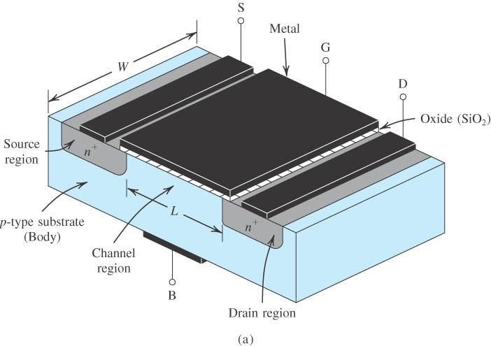
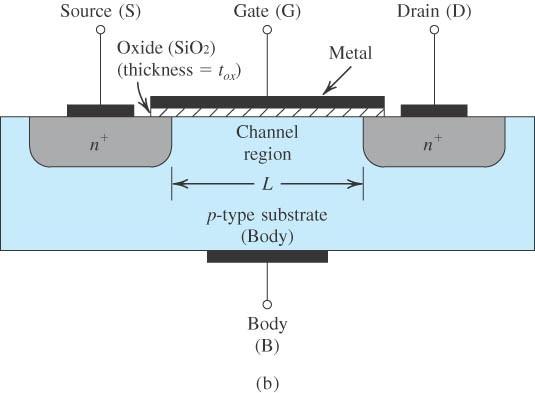
3 NMOS Enhancement Device 3

4 Establishing a Channel v GS V t v DS =0 v GD =v GS v DS =v GS C ox = ox t ox F /cm 2 C gb =C ox WLF 4

5 Acts as a Voltage-Controlled Resistor v GD =v GS v DS v GS 5

6 NMOS Operation as v DS Increases 1. For small v DS : v GD =v GS v DS v GS 2. As v DS is increased for fixed v GS : v GD=v GS v DS -> decreases 3. When v DS =v DSsat =v GS V t v GD =V t channel pinches off at drain-end 4. As v DS is increased v DS v DSsat =v GS V t v GD V t channel L decreases. 6
7 Curve Flattens With Increased v DS 7
8 NMOS Enhancement Model Background If v GS V t,the drain to source current, i DS, increases until: v DS v GS V t The MOSFET saturates at this value of v DS and (except for an Early Effect ) i DS does not increase with further increases in v DS. This channel current is proportional to the channel width W, inversely proportional to its length L, and proportional to its transconductance parameter, k' n : ' k n = n C ox = cm2 V sec F cm2 C /V = 2 cm V sec cm = A 2 V 2 C ox is the capacitance per unit area of the gate-channel interface and n is the fabrication-dependent channel electron mobility. 8
9 Uniform Channel Width (Small v DS ) Model Drain-to-source current with fixed gate-to-source voltage is proportional to drain to source voltage: g DS =k n L v GS V t i D =i DS =g DS v DS =k n L v GS V t v DS r DS =1/ g DS = voltage-controlled resistance k n Intuitively, conductance g DS is proportional to the conductor cross-section - channel width, W, times channel depth (set by the gate to source voltage, v GS -V t ) and the conductivity of the channel material. Conductance is inversely proportional to L, the length of the current path. 1 L v GS V t 9
10 NMOS Enhancement Model Structure A satisfactory v DS - i DS model for the triode region is a quadratic expression that is linear for small v DS and reaches a maximum where the device saturates: Small v DS, where i D =i DS =k n L [ v GS V t v DS 1 2 v DS Saturation, where v DS =v GS V t : i D =i DS =k n 2 ] 1 2 v 2 v V v : DS i =i =k GS t DS D DS n L v GS V t v DS [ L v GS V t v GS V t 1 2] 2 v GS V t = k ' n 2 i D =i DS = k ' n 2 W L v GS V t 2 Triode region W L v GS V t 2 Saturation region 10
11 NMOS Enhancement Models For the NMOS enhancement mode (strong-inversion) transistor: For: For: v GS V t 0 i DS =0 v GS V t 0 (Channel non-existent) (Channel exists) v DS v GS V t 2 ] i D =i DS =k n L [ v GS V t v DS 1 2 v DS (Triode) v DS v GS V t i D =i DS = 1 2 k n L v V GS t 2 (Saturation) 11
12 Channel Length Modulation v DS v DSsat =v GS V t v GD V t L= Lv DS process parameter withunits V 1 Modify the saturation model to account for L: i D =i DS = 1 2 k n L v GS V t k n L L v GS V t 2 = 1 2 k n L L L 1 L 1 L/ L v GS V t 2 i D =i DS 1 2 k n L 1 L L v GS V t 2 = 1 2 k n L v GS V t 2 1 n v DS 12
13 V A Early Voltage Relation to Lambda Saturation: i D =i DS 1 2 k n L v GS V t 2 1 n v DS small-signal output-resistance r o = V A I D = 1 I D where I D = 1 2 k n L V GS V t 2 slope=1/r o V A = 1 Triode: [ i D =i DS k n L v GS V t v DS 1 2 v ] 2 1 DS nv DS 13
14 NMOS Enhancement Circuit Symbols Sedra Symbols Multisim Symbols The body diode is indicated by the B terminal arrow. The substrate typically is connected to the most negative circuit voltage so the body diode is back biased. 14

15 NMOS Physical Representations 15

16 PMOS Enhancement Device PMOS Transistor on a p-type body (CMOS circuit). NOTE: p-type body is substrate for NMOS transistor n-well is local substrate for PMOS transistor 16
17 PMOS Enhancement Model PMOS device model is NMOS model with all polarities reversed: For: For: v SG V 0 t i D =i SD =0 v SG V 0 t v SD v SG V t (Channel non-existent) (Channel exists) [ i D =i SD =k p L v SG V t v SD 1 2 v ] 2 1 SD p v SD v SD v SG V t i D =i SD = 1 2 k p L v SG V 2 t 1 p v SD (Triode) (Saturation) 17
18 PMOS Enhancement Circuit Symbols Sedra Symbols Multisim Symbols another PMOS symbol 18
 v gs g m v gs r o g m= 2 nc ox")
 V gs C gs g m V gs r")
19 nmos Small Signal Model Low Frequency (approximate) v gs g m v gs r o g m= 2 nc ox W L I D r o = 1 n I D C gd C gs C High Frequency (approximate) V gs C gs g m V gs r o C gd C 19
ECE 342 Electronic Circuits. Lecture 6 MOS Transistors
 ECE 342 Electronic Circuits Lecture 6 MOS Transistors Jose E. Schutt-Aine Electrical & Computer Engineering University of Illinois jesa@illinois.edu 1 NMOS Transistor Typically L = 0.1 to 3 m, W = 0.2
EE105 - Fall 2005 Microelectronic Devices and Circuits
 EE105 - Fall 005 Microelectronic Devices and Circuits ecture 7 MOS Transistor Announcements Homework 3, due today Homework 4 due next week ab this week Reading: Chapter 4 1 ecture Material ast lecture
Practice 3: Semiconductors
 Practice 3: Semiconductors Digital Electronic Circuits Semester A 2012 VLSI Fabrication Process VLSI Very Large Scale Integration The ability to fabricate many devices on a single substrate within a given
The Devices. Digital Integrated Circuits A Design Perspective. Jan M. Rabaey Anantha Chandrakasan Borivoje Nikolic. July 30, 2002
 Digital Integrated Circuits A Design Perspective Jan M. Rabaey Anantha Chandrakasan Borivoje Nikolic The Devices July 30, 2002 Goal of this chapter Present intuitive understanding of device operation Introduction
MOSFET: Introduction
 E&CE 437 Integrated VLSI Systems MOS Transistor 1 of 30 MOSFET: Introduction Metal oxide semiconductor field effect transistor (MOSFET) or MOS is widely used for implementing digital designs Its major
Lecture 3: CMOS Transistor Theory
 Lecture 3: CMOS Transistor Theory Outline Introduction MOS Capacitor nmos I-V Characteristics pmos I-V Characteristics Gate and Diffusion Capacitance 2 Introduction So far, we have treated transistors
Microelectronics Part 1: Main CMOS circuits design rules
 GBM8320 Dispositifs Médicaux telligents Microelectronics Part 1: Main CMOS circuits design rules Mohamad Sawan et al. Laboratoire de neurotechnologies Polystim! http://www.cours.polymtl.ca/gbm8320/! med-amine.miled@polymtl.ca!
Integrated Circuits & Systems
 Federal University of Santa Catarina Center for Technology Computer Science & Electronics Engineering Integrated Circuits & Systems INE 5442 Lecture 10 MOSFET part 1 guntzel@inf.ufsc.br ual-well Trench-Isolated
Introduction and Background
 Analog CMOS Integrated Circuit Design Introduction and Background Dr. Jawdat Abu-Taha Department of Electrical and Computer Engineering Islamic University of Gaza jtaha@iugaza.edu.ps 1 Marking Assignments
CMPEN 411 VLSI Digital Circuits. Lecture 03: MOS Transistor
 CMPEN 411 VLSI Digital Circuits Lecture 03: MOS Transistor Kyusun Choi [Adapted from Rabaey s Digital Integrated Circuits, Second Edition, 2003 J. Rabaey, A. Chandrakasan, B. Nikolic] CMPEN 411 L03 S.1
EE382M-14 CMOS Analog Integrated Circuit Design
 EE382M-14 CMOS Analog Integrated Circuit Design Lecture 3, MOS Capacitances, Passive Components, and Layout of Analog Integrated Circuits MOS Capacitances Type of MOS transistor capacitors Depletion capacitance
ECE 342 Electronic Circuits. 3. MOS Transistors
 ECE 342 Electronic Circuits 3. MOS Transistors Jose E. Schutt-Aine Electrical & Computer Engineering University of Illinois jschutt@emlab.uiuc.edu 1 NMOS Transistor Typically L = 0.1 to 3 m, W = 0.2 to
Quantitative MOSFET. Step 1. Connect the MOS capacitor results for the electron charge in the inversion layer Q N to the drain current.
 Quantitative MOSFET Step 1. Connect the MOS capacitor results for the electron charge in the inversion layer Q N to the drain current. V DS _ n source polysilicon gate y = y * 0 x metal interconnect to
Lecture 12: MOSFET Devices
 Lecture 12: MOSFET Devices Gu-Yeon Wei Division of Engineering and Applied Sciences Harvard University guyeon@eecs.harvard.edu Wei 1 Overview Reading S&S: Chapter 5.1~5.4 Supplemental Reading Background
MOS Transistor I-V Characteristics and Parasitics
 ECEN454 Digital Integrated Circuit Design MOS Transistor I-V Characteristics and Parasitics ECEN 454 Facts about Transistors So far, we have treated transistors as ideal switches An ON transistor passes
II III IV V VI B C N. Al Si P S. Zn Ga Ge As Se Cd In Sn Sb Te. Silicon (Si) the dominating material in IC manufacturing
 the dominating material in IC manufacturing") II III IV V VI B N Al Si P S Zn Ga Ge As Se d In Sn Sb Te Silicon (Si) the dominating material in I manufacturing ompound semiconductors III - V group: GaAs GaN GaSb GaP InAs InP InSb... The Energy Band
II III IV V VI B N Al Si P S Zn Ga Ge As Se d In Sn Sb Te Silicon (Si) the dominating material in I manufacturing ompound semiconductors III - V group: GaAs GaN GaSb GaP InAs InP InSb... The Energy Band
EE105 - Fall 2006 Microelectronic Devices and Circuits
 EE105 - Fall 2006 Microelectronic Devices and Circuits Prof. Jan M. Rabaey (jan@eecs) Lecture 7: MOS Transistor Some Administrative Issues Lab 2 this week Hw 2 due on We Hw 3 will be posted same day MIDTERM
EE115C Winter 2017 Digital Electronic Circuits. Lecture 3: MOS RC Model, CMOS Manufacturing
 EE115C Winter 2017 Digital Electronic Circuits Lecture 3: MOS RC Model, CMOS Manufacturing Agenda MOS Transistor: RC Model (pp. 104-113) S R on D CMOS Manufacturing Process (pp. 36-46) S S C GS G G C GD
Lecture 4: CMOS Transistor Theory
 Introduction to CMOS VLSI Design Lecture 4: CMOS Transistor Theory David Harris, Harvey Mudd College Kartik Mohanram and Steven Levitan University of Pittsburgh Outline q Introduction q MOS Capacitor q
Digital Integrated Circuits A Design Perspective. Jan M. Rabaey Anantha Chandrakasan Borivoje Nikolic. The Devices. July 30, Devices.
 Digital Integrated Circuits A Design Perspective Jan M. Rabaey Anantha Chandrakasan Borivoje Nikolic The July 30, 2002 1 Goal of this chapter Present intuitive understanding of device operation Introduction
MOS Transistor Theory
 MOS Transistor Theory So far, we have viewed a MOS transistor as an ideal switch (digital operation) Reality: less than ideal EE 261 Krish Chakrabarty 1 Introduction So far, we have treated transistors
Chapter 4 Field-Effect Transistors
 Chapter 4 Field-Effect Transistors Microelectronic Circuit Design Richard C. Jaeger Travis N. Blalock 5/5/11 Chap 4-1 Chapter Goals Describe operation of MOSFETs. Define FET characteristics in operation
EEC 118 Lecture #2: MOSFET Structure and Basic Operation. Rajeevan Amirtharajah University of California, Davis Jeff Parkhurst Intel Corporation
 EEC 118 Lecture #2: MOSFET Structure and Basic Operation Rajeevan Amirtharajah University of California, Davis Jeff Parkhurst Intel Corporation Announcements Lab 1 this week, report due next week Bring
Device Models (PN Diode, MOSFET )
") Device Models (PN Diode, MOSFET ) Instructor: Steven P. Levitan steve@ece.pitt.edu TA: Gayatri Mehta, José Martínez Book: Digital Integrated Circuits: A Design Perspective; Jan Rabaey Lab Notes: Handed
Device Models (PN Diode, MOSFET ) Instructor: Steven P. Levitan steve@ece.pitt.edu TA: Gayatri Mehta, José Martínez Book: Digital Integrated Circuits: A Design Perspective; Jan Rabaey Lab Notes: Handed
Today s lecture. EE141- Spring 2003 Lecture 4. Design Rules CMOS Inverter MOS Transistor Model
 - Spring 003 Lecture 4 Design Rules CMOS Inverter MOS Transistor Model Today s lecture Design Rules The CMOS inverter at a glance An MOS transistor model for manual analysis Important! Labs start next
Lecture 11: MOS Transistor
 Lecture 11: MOS Transistor Prof. Niknejad Lecture Outline Review: MOS Capacitors Regions MOS Capacitors (3.8 3.9) CV Curve Threshold Voltage MOS Transistors (4.1 4.3): Overview Cross-section and layout
MOSFET Physics: The Long Channel Approximation
 MOSFET Physics: The ong Channel Approximation A basic n-channel MOSFET (Figure 1) consists of two heavily-doped n-type regions, the Source and Drain, that comprise the main terminals of the device. The
Lecture 15: MOS Transistor models: Body effects, SPICE models. Context. In the last lecture, we discussed the modes of operation of a MOS FET:
 Lecture 15: MOS Transistor models: Body effects, SPICE models Context In the last lecture, we discussed the modes of operation of a MOS FET: oltage controlled resistor model I- curve (Square-Law Model)
Introduction to CMOS VLSI. Chapter 2: CMOS Transistor Theory. Harris, 2004 Updated by Li Chen, Outline
 Introduction to MOS VLSI Design hapter : MOS Transistor Theory copyright@david Harris, 004 Updated by Li hen, 010 Outline Introduction MOS apacitor nmos IV haracteristics pmos IV haracteristics Gate and
The Devices. Devices
 The The MOS Transistor Gate Oxyde Gate Source n+ Polysilicon Drain n+ Field-Oxyde (SiO 2 ) p-substrate p+ stopper Bulk Contact CROSS-SECTION of NMOS Transistor Cross-Section of CMOS Technology MOS transistors
The Gradual Channel Approximation for the MOSFET:
 6.01 - Electronic Devices and Circuits Fall 003 The Gradual Channel Approximation for the MOSFET: We are modeling the terminal characteristics of a MOSFET and thus want i D (v DS, v GS, v BS ), i B (v
Lecture 12: MOS Capacitors, transistors. Context
 Lecture 12: MOS Capacitors, transistors Context In the last lecture, we discussed PN diodes, and the depletion layer into semiconductor surfaces. Small signal models In this lecture, we will apply those
The Devices. Digital Integrated Circuits A Design Perspective. Jan M. Rabaey Anantha Chandrakasan Borivoje Nikolic. July 30, 2002
 igital Integrated Circuits A esign Perspective Jan M. Rabaey Anantha Chandrakasan Borivoje Nikolic The evices July 30, 2002 Goal of this chapter Present intuitive understanding of device operation Introduction
ECE 546 Lecture 10 MOS Transistors
 ECE 546 Lecture 10 MOS Transistors Spring 2018 Jose E. Schutt-Aine Electrical & Computer Engineering University of Illinois jesa@illinois.edu NMOS Transistor NMOS Transistor N-Channel MOSFET Built on p-type
Operation and Modeling of. The MOS Transistor. Second Edition. Yannis Tsividis Columbia University. New York Oxford OXFORD UNIVERSITY PRESS
 Operation and Modeling of The MOS Transistor Second Edition Yannis Tsividis Columbia University New York Oxford OXFORD UNIVERSITY PRESS CONTENTS Chapter 1 l.l 1.2 1.3 1.4 1.5 1.6 1.7 Chapter 2 2.1 2.2
6.012 Electronic Devices and Circuits Spring 2005
 6.012 Electronic Devices and Circuits Spring 2005 May 16, 2005 Final Exam (200 points) -OPEN BOOK- Problem NAME RECITATION TIME 1 2 3 4 5 Total General guidelines (please read carefully before starting):
The Devices. Jan M. Rabaey
 The Devices Jan M. Rabaey Goal of this chapter Present intuitive understanding of device operation Introduction of basic device equations Introduction of models for manual analysis Introduction of models
The Devices: MOS Transistors
 The Devices: MOS Transistors References: Semiconductor Device Fundamentals, R. F. Pierret, Addison-Wesley Digital Integrated Circuits: A Design Perspective, J. Rabaey et.al. Prentice Hall NMOS Transistor
Fig. 1 CMOS Transistor Circuits (a) Inverter Out = NOT In, (b) NOR-gate C = NOT (A or B)
 Inverter Out = NOT In, (b) NOR-gate C = NOT (A or B)") 1 Introduction to Transistor-Level Logic Circuits 1 By Prawat Nagvajara At the transistor level of logic circuits, transistors operate as switches with the logic variables controlling the open or closed
1 Introduction to Transistor-Level Logic Circuits 1 By Prawat Nagvajara At the transistor level of logic circuits, transistors operate as switches with the logic variables controlling the open or closed
EE105 Fall 2014 Microelectronic Devices and Circuits. NMOS Transistor Capacitances: Saturation Region
 EE105 Fall 014 Microelectronic Devices and Circuits Prof. Ming C. Wu wu@eecs.berkeley.edu 511 Sutardja Dai Hall (SDH) 1 NMOS Transistor Capacitances: Saturation Region Drain no longer connected to channel
3. Design a stick diagram for the PMOS logic shown below [16] Y = (A + B).C. 4. Design a layout diagram for the CMOS logic shown below [16]
![3. Design a stick diagram for the PMOS logic shown below [16] Y = (A + B).C. 4. Design a layout diagram for the CMOS logic shown below [16]](/thumbs/96/128765118.jpg "3. Design a stick diagram for the PMOS logic shown below [16] Y = (A + B).C. 4. Design a layout diagram for the CMOS logic shown below [16]") Code No: RR420203 Set No. 1 1. (a) Find g m and r ds for an n-channel transistor with V GS = 1.2V; V tn = 0.8V; W/L = 10; µncox = 92 µa/v 2 and V DS = Veff + 0.5V The out put impedance constant. λ = 95.3
Code No: RR420203 Set No. 1 1. (a) Find g m and r ds for an n-channel transistor with V GS = 1.2V; V tn = 0.8V; W/L = 10; µncox = 92 µa/v 2 and V DS = Veff + 0.5V The out put impedance constant. λ = 95.3
Course Administration. CPE/EE 427, CPE 527 VLSI Design I L04: MOS Transistors. Review: CMOS Process at a Glance
 Course Administration CPE/EE 7, CPE 7 VLI esign I L: MO Transistors epartment of Electrical and Computer Engineering University of Alabama in Huntsville Aleksandar Milenkovic ( www.ece.uah.edu/~milenka
Section 12: Intro to Devices
 Section 12: Intro to Devices Extensive reading materials on reserve, including Robert F. Pierret, Semiconductor Device Fundamentals EE143 Ali Javey Bond Model of Electrons and Holes Si Si Si Si Si Si Si
MOS Transistors. Prof. Krishna Saraswat. Department of Electrical Engineering Stanford University Stanford, CA
 MOS Transistors Prof. Krishna Saraswat Department of Electrical Engineering S Stanford, CA 94305 saraswat@stanford.edu 1 1930: Patent on the Field-Effect Transistor! Julius Lilienfeld filed a patent describing
ESE 570: Digital Integrated Circuits and VLSI Fundamentals
 ESE 570: Digital Integrated Circuits and VLSI Fundamentals Lec 4: January 23, 2018 MOS Transistor Theory, MOS Model Penn ESE 570 Spring 2018 Khanna Lecture Outline! CMOS Process Enhancements! Semiconductor
ELEC 3908, Physical Electronics, Lecture 23. The MOSFET Square Law Model
 ELEC 3908, Physical Electronics, Lecture 23 The MOSFET Square Law Model Lecture Outline As with the diode and bipolar, have looked at basic structure of the MOSFET and now turn to derivation of a current
Microelectronics Main CMOS design rules & basic circuits
 GBM8320 Dispositifs médicaux intelligents Microelectronics Main CMOS design rules & basic circuits Mohamad Sawan et al. Laboratoire de neurotechnologies Polystim mohamad.sawan@polymtl.ca M5418 6 & 7 September
EE 560 MOS TRANSISTOR THEORY PART 2. Kenneth R. Laker, University of Pennsylvania
 1 EE 560 MOS TRANSISTOR THEORY PART nmos TRANSISTOR IN LINEAR REGION V S = 0 V G > V T0 channel SiO V D = small 4 C GC C BC substrate depletion region or bulk B p nmos TRANSISTOR AT EDGE OF SATURATION
Chapter 2 CMOS Transistor Theory. Jin-Fu Li Department of Electrical Engineering National Central University Jungli, Taiwan
 Chapter 2 CMOS Transistor Theory Jin-Fu Li Department of Electrical Engineering National Central University Jungli, Taiwan Outline Introduction MOS Device Design Equation Pass Transistor Jin-Fu Li, EE,
SECTION: Circle one: Alam Lundstrom. ECE 305 Exam 5 SOLUTIONS: Spring 2016 April 18, 2016 M. A. Alam and M.S. Lundstrom Purdue University
 NAME: PUID: SECTION: Circle one: Alam Lundstrom ECE 305 Exam 5 SOLUTIONS: April 18, 2016 M A Alam and MS Lundstrom Purdue University This is a closed book exam You may use a calculator and the formula
Studio 3 Review MOSFET as current source Small V DS : Resistor (value controlled by V GS ) Large V DS : Current source (value controlled by V GS )
 Large V DS : Current source (value controlled by V GS )") Studio 3 Review MOSFET as current source Small V DS : Resistor (value controlled by V GS ) Large V DS : Current source (value controlled by V GS ) 1 Simulation Review: Circuit Fixed V GS, Sweep V DS I
Studio 3 Review MOSFET as current source Small V DS : Resistor (value controlled by V GS ) Large V DS : Current source (value controlled by V GS ) 1 Simulation Review: Circuit Fixed V GS, Sweep V DS I
P. R. Nelson 1 ECE418 - VLSI. Midterm Exam. Solutions
 P. R. Nelson 1 ECE418 - VLSI Midterm Exam Solutions 1. (8 points) Draw the cross-section view for A-A. The cross-section view is as shown below.. ( points) Can you tell which of the metal1 regions is the
Field-Effect (FET) transistors
 transistors") Field-Effect (FET) transistors References: Barbow (Chapter 8), Rizzoni (chapters 8 & 9) In a field-effect transistor (FET), the width of a conducting channel in a semiconductor and, therefore, its current-carrying
Field-Effect (FET) transistors References: Barbow (Chapter 8), Rizzoni (chapters 8 & 9) In a field-effect transistor (FET), the width of a conducting channel in a semiconductor and, therefore, its current-carrying
Lecture 9 MOSFET(II) MOSFET I V CHARACTERISTICS(contd.)
 MOSFET I V CHARACTERISTICS(contd.)") Lecture 9 MOSFET(II) MOSFET I V CHARACTERISTICS(contd.) Outline 1. The saturation region 2. Backgate characteristics Reading Assignment: Howe and Sodini, Chapter 4, Section 4.4 6.012 Spring 2009 Lecture
Lecture 9 MOSFET(II) MOSFET I V CHARACTERISTICS(contd.) Outline 1. The saturation region 2. Backgate characteristics Reading Assignment: Howe and Sodini, Chapter 4, Section 4.4 6.012 Spring 2009 Lecture
VLSI Design I; A. Milenkovic 1
 Review: implified CMO Inverter Process CPE/EE 7, CPE 7 VLI esign I L: MO Transistor cut line epartment of Electrical and Computer Engineering University of Alabama in Huntsville Aleksandar Milenkovic (
Lecture 210 Physical Aspects of ICs (12/15/01) Page 210-1
 Page 210-1") Lecture 210 Physical Aspects of ICs (12/15/01) Page 210-1 LECTURE 210 PHYSICAL ASPECTS OF ICs (READING: Text-Sec. 2.5, 2.6, 2.8) INTRODUCTION Objective Illustrate the physical aspects of integrated circuits
Lecture 210 Physical Aspects of ICs (12/15/01) Page 210-1 LECTURE 210 PHYSICAL ASPECTS OF ICs (READING: Text-Sec. 2.5, 2.6, 2.8) INTRODUCTION Objective Illustrate the physical aspects of integrated circuits
LECTURE 3 MOSFETS II. MOS SCALING What is Scaling?
 LECTURE 3 MOSFETS II Lecture 3 Goals* * Understand constant field and constant voltage scaling and their effects. Understand small geometry effects for MOS transistors and their implications modeling and
Lecture 5: CMOS Transistor Theory
 Lecture 5: CMOS Transistor Theory Slides courtesy of Deming Chen Slides based on the initial set from David Harris CMOS VLSI Design Outline q q q q q q q Introduction MOS Capacitor nmos I-V Characteristics
MOS Transistor Theory
 CHAPTER 3 MOS Transistor Theory Outline 2 1. Introduction 2. Ideal I-V Characteristics 3. Nonideal I-V Effects 4. C-V Characteristics 5. DC Transfer Characteristics 6. Switch-level RC Delay Models MOS
ECE 415/515 ANALOG INTEGRATED CIRCUIT DESIGN
 ECE 415/515 ANALOG INTEGRATED CIRCUIT DESIGN CMOS PROCESS CHARACTERIZATION VISHAL SAXENA VSAXENA@UIDAHO.EDU Vishal Saxena DESIGN PARAMETERS Analog circuit designers care about: Open-loop Gain: g m r o
ELEC 3908, Physical Electronics, Lecture 26. MOSFET Small Signal Modelling
 ELEC 3908, Physical Electronics, Lecture 26 MOSFET Small Signal Modelling Lecture Outline MOSFET small signal behavior will be considered in the same way as for the diode and BJT Capacitances will be considered
FIELD-EFFECT TRANSISTORS
 FIEL-EFFECT TRANSISTORS 1 Semiconductor review 2 The MOS capacitor 2 The enhancement-type N-MOS transistor 3 I-V characteristics of enhancement MOSFETS 4 The output characteristic of the MOSFET in saturation
Extensive reading materials on reserve, including
 Section 12: Intro to Devices Extensive reading materials on reserve, including Robert F. Pierret, Semiconductor Device Fundamentals EE143 Ali Javey Bond Model of Electrons and Holes Si Si Si Si Si Si Si
Lecture 0: Introduction
 Lecture 0: Introduction Introduction q Integrated circuits: many transistors on one chip q Very Large Scale Integration (VLSI): bucketloads! q Complementary Metal Oxide Semiconductor Fast, cheap, low power
Lecture 04 Review of MOSFET
 ECE 541/ME 541 Microelectronic Fabrication Techniques Lecture 04 Review of MOSFET Zheng Yang (ERF 3017, email: yangzhen@uic.edu) What is a Transistor? A Switch! An MOS Transistor V GS V T V GS S Ron D
EE 330 Lecture 16. MOS Device Modeling p-channel n-channel comparisons Model consistency and relationships CMOS Process Flow
 EE 330 Lecture 16 MOS Device Modeling p-channel n-channel comparisons Model consistency and relationships CMOS Process Flow Review from Last Time Operation Regions by Applications Id I D 300 250 200 150
The Physical Structure (NMOS)
") The Physical Structure (NMOS) Al SiO2 Field Oxide Gate oxide S n+ Polysilicon Gate Al SiO2 SiO2 D n+ L channel P Substrate Field Oxide contact Metal (S) n+ (G) L W n+ (D) Poly 1 Transistor Resistance Two
The Physical Structure (NMOS) Al SiO2 Field Oxide Gate oxide S n+ Polysilicon Gate Al SiO2 SiO2 D n+ L channel P Substrate Field Oxide contact Metal (S) n+ (G) L W n+ (D) Poly 1 Transistor Resistance Two
Lecture 13 MOSFET as an amplifier with an introduction to MOSFET small-signal model and small-signal schematics. Lena Peterson
 Lecture 13 MOSFET as an amplifier with an introduction to MOSFET small-signal model and small-signal schematics Lena Peterson 2015-10-13 Outline (1) Why is the CMOS inverter gain not infinite? Large-signal
Figure 1: MOSFET symbols.
 c Copyright 2008. W. Marshall Leach, Jr., Professor, Georgia Institute of Technology, School of Electrical and Computer Engineering. The MOSFET Device Symbols Whereas the JFET has a diode junction between
nmos IC Design Report Module: EEE 112
 nmos IC Design Report Author: 1302509 Zhao Ruimin Module: EEE 112 Lecturer: Date: Dr.Zhao Ce Zhou June/5/2015 Abstract This lab intended to train the experimental skills of the layout designing of the
MOS Transistor Theory MOSFET Symbols Current Characteristics of MOSFET. MOS Symbols and Characteristics. nmos Enhancement Transistor
 MOS Transistor Theory MOSFET Symbols Current Characteristics of MOSFET Calculation of t and Important 2 nd Order Effects SmallSignal Signal MOSFET Model Summary Material from: CMOS LSI Design By Weste
ELEN0037 Microelectronic IC Design. Prof. Dr. Michael Kraft
 ELEN0037 Microelectronic IC Design Prof. Dr. Michael Kraft Lecture 2: Technological Aspects Technology Passive components Active components CMOS Process Basic Layout Scaling CMOS Technology Integrated
EE 560 MOS TRANSISTOR THEORY
 1 EE 560 MOS TRANSISTOR THEORY PART 1 TWO TERMINAL MOS STRUCTURE V G (GATE VOLTAGE) 2 GATE OXIDE SiO 2 SUBSTRATE p-type doped Si (N A = 10 15 to 10 16 cm -3 ) t ox V B (SUBSTRATE VOLTAGE) EQUILIBRIUM:
AE74 VLSI DESIGN JUN 2015
 Q.2 a. Write down the different levels of integration of IC industry. (4) b. With neat sketch explain briefly PMOS & NMOS enhancement mode transistor. N-MOS enhancement mode transistor:- This transistor
! CMOS Process Enhancements. ! Semiconductor Physics. " Band gaps. " Field Effects. ! MOS Physics. " Cut-off. " Depletion.
 ESE 570: Digital Integrated Circuits and VLSI Fundamentals Lec 4: January 3, 018 MOS Transistor Theory, MOS Model Lecture Outline! CMOS Process Enhancements! Semiconductor Physics " Band gaps " Field Effects!
University of Pennsylvania Department of Electrical Engineering. ESE 570 Midterm Exam March 14, 2013 FORMULAS AND DATA
 University of Pennsylvania Department of Electrical Engineering ESE 570 Midterm Exam March 4, 03 FORMULAS AND DATA. PHYSICAL CONSTANTS: n i = intrinsic concentration undoped) silicon =.45 x 0 0 cm -3 @
ECEN474/704: (Analog) VLSI Circuit Design Spring 2018
 VLSI Circuit Design Spring 2018") ECEN474/704: (Analog) SI Circuit Design Spring 2018 ecture 2: MOS ransistor Modeling Sam Palermo Analog & Mixed-Signal Center exas A&M University Announcements If you haven t already, turn in your 0.18um
ECEN474/704: (Analog) SI Circuit Design Spring 2018 ecture 2: MOS ransistor Modeling Sam Palermo Analog & Mixed-Signal Center exas A&M University Announcements If you haven t already, turn in your 0.18um
MOS Capacitors ECE 2204
 MOS apacitors EE 2204 Some lasses of Field Effect Transistors Metal-Oxide-Semiconductor Field Effect Transistor MOSFET, which will be the type that we will study in this course. Metal-Semiconductor Field
HW 5 posted due in two weeks Lab this week Midterm graded Project to be launched in week 7
 HW 5 posted due in two weeks Lab this week Midterm graded Project to be launched in week 7 2 What do digital IC designers need to know? 5 EE4 EECS4 6 3 0< V GS - V T < V DS Pinch-off 7 For (V GS V T )
CMPEN 411 VLSI Digital Circuits. Lecture 04: CMOS Inverter (static view)
") CMPEN 411 VLSI Digital Circuits Lecture 04: CMOS Inverter (static view) Kyusun Choi [Adapted from Rabaey s Digital Integrated Circuits, Second Edition, 2003 J. Rabaey, A. Chandrakasan, B. Nikolic] CMPEN
CMPEN 411 VLSI Digital Circuits Lecture 04: CMOS Inverter (static view) Kyusun Choi [Adapted from Rabaey s Digital Integrated Circuits, Second Edition, 2003 J. Rabaey, A. Chandrakasan, B. Nikolic] CMPEN
Lecture 15 OUTLINE. MOSFET structure & operation (qualitative) Review of electrostatics The (N)MOS capacitor
 Review of electrostatics The (N)MOS capacitor") Lecture 15 OUTLINE MOSFET structure & operation (qualitative) Review of electrostatics The (N)MOS capacitor Electrostatics t ti Charge vs. voltage characteristic Reading: Chapter 6.1 6.2.1 EE105 Fall 2007
Lecture 15 OUTLINE MOSFET structure & operation (qualitative) Review of electrostatics The (N)MOS capacitor Electrostatics t ti Charge vs. voltage characteristic Reading: Chapter 6.1 6.2.1 EE105 Fall 2007
Lecture Outline. ESE 570: Digital Integrated Circuits and VLSI Fundamentals. Review: MOS Capacitor with External Bias
 ESE 57: Digital Integrated Circuits and VLSI Fundamentals Lec 5: Januar 6, 17 MOS Operating Regions, pt. 1 Lecture Outline! 3 Regions of operation for MOSFET " Subthreshold " Linear " Saturation! Level
VLSI Design The MOS Transistor
 VLSI Design The MOS Transistor Frank Sill Torres Universidade Federal de Minas Gerais (UFMG), Brazil VLSI Design: CMOS Technology 1 Outline Introduction MOS Capacitor nmos I-V Characteristics pmos I-V
Metal-oxide-semiconductor field effect transistors (2 lectures)
") Metal-ide-semiconductor field effect transistors ( lectures) MOS physics (brief in book) Current-voltage characteristics - pinch-off / channel length modulation - weak inversion - velocity saturation -
Metal-ide-semiconductor field effect transistors ( lectures) MOS physics (brief in book) Current-voltage characteristics - pinch-off / channel length modulation - weak inversion - velocity saturation -
ECE 497 JS Lecture - 12 Device Technologies
 ECE 497 JS Lecture - 12 Device Technologies Spring 2004 Jose E. Schutt-Aine Electrical & Computer Engineering University of Illinois jose@emlab.uiuc.edu 1 NMOS Transistor 2 ρ Source channel charge density
EE 330 Lecture 16. MOSFET Modeling CMOS Process Flow
 EE 330 Lecture 16 MOSFET Modeling CMOS Process Flow Model Extensions 300 Id 250 200 150 100 50 300 0 0 1 2 3 4 5 Vds Existing Model 250 200 Id 150 100 50 Slope is not 0 0 0 1 2 3 4 Actual Device Vds Model
VLSI Design and Simulation
 VLSI Design and Simulation Performance Characterization Topics Performance Characterization Resistance Estimation Capacitance Estimation Inductance Estimation Performance Characterization Inverter Voltage
ECE321 Electronics I
 EE31 Electronics I Lecture 8: MOSET Threshold Voltage and Parasitic apacitances Payman Zarkesh-Ha Office: EE Bldg. 3B Office hours: Tuesday :-3:PM or by appointment E-mail: payman@ece.unm.edu Slide: 1
! PN Junction. ! MOS Transistor Topology. ! Threshold. ! Operating Regions. " Resistive. " Saturation. " Subthreshold (next class)
") ESE370: ircuitlevel Modeling, Design, and Optimization for Digital Systems Lec 7: September 20, 2017 MOS Transistor Operating Regions Part 1 Today! PN Junction! MOS Transistor Topology! Threshold! Operating
ESE370: ircuitlevel Modeling, Design, and Optimization for Digital Systems Lec 7: September 20, 2017 MOS Transistor Operating Regions Part 1 Today! PN Junction! MOS Transistor Topology! Threshold! Operating
ECE-305: Fall 2017 MOS Capacitors and Transistors
 ECE-305: Fall 2017 MOS Capacitors and Transistors Pierret, Semiconductor Device Fundamentals (SDF) Chapters 15+16 (pp. 525-530, 563-599) Professor Peter Bermel Electrical and Computer Engineering Purdue
Lecture 15 OUTLINE. MOSFET structure & operation (qualitative) Review of electrostatics The (N)MOS capacitor
 Review of electrostatics The (N)MOS capacitor") Lecture 15 OUTLINE MOSFET structure & operation (qualitative) Review of electrostatics The (N)MOS capacitor Electrostatics Charge vs. voltage characteristic Reading: Chapter 6.1 6.2.1 EE15 Spring 28 Lecture
Lecture 15 OUTLINE MOSFET structure & operation (qualitative) Review of electrostatics The (N)MOS capacitor Electrostatics Charge vs. voltage characteristic Reading: Chapter 6.1 6.2.1 EE15 Spring 28 Lecture
Fundamentals of the Metal Oxide Semiconductor Field-Effect Transistor
 Triode Working FET Fundamentals of the Metal Oxide Semiconductor Field-Effect Transistor The characteristics of energy bands as a function of applied voltage. Surface inversion. The expression for the
VLSI VLSI CIRCUIT DESIGN PROCESSES P.VIDYA SAGAR ( ASSOCIATE PROFESSOR) Department of Electronics and Communication Engineering, VBIT
 Department of Electronics and Communication Engineering, VBIT") VLSI VLSI CIRCUIT DESIGN PROCESSES P.VIDYA SAGAR ( ASSOCIATE PROFESSOR) SYLLABUS UNIT II VLSI CIRCUIT DESIGN PROCESSES: VLSI Design Flow, MOS Layers, Stick Diagrams, Design Rules and Layout, 2 m CMOS Design
VLSI VLSI CIRCUIT DESIGN PROCESSES P.VIDYA SAGAR ( ASSOCIATE PROFESSOR) SYLLABUS UNIT II VLSI CIRCUIT DESIGN PROCESSES: VLSI Design Flow, MOS Layers, Stick Diagrams, Design Rules and Layout, 2 m CMOS Design
Lecture 150 Basic IC Processes (10/10/01) Page ECE Analog Integrated Circuits and Systems P.E. Allen
 Page ECE Analog Integrated Circuits and Systems P.E. Allen") Lecture 150 Basic IC Processes (10/10/01) Page 1501 LECTURE 150 BASIC IC PROCESSES (READING: TextSec. 2.2) INTRODUCTION Objective The objective of this presentation is: 1.) Introduce the fabrication of
Lecture 150 Basic IC Processes (10/10/01) Page 1501 LECTURE 150 BASIC IC PROCESSES (READING: TextSec. 2.2) INTRODUCTION Objective The objective of this presentation is: 1.) Introduce the fabrication of
CMOS INVERTER. Last Lecture. Metrics for qualifying digital circuits. »Cost» Reliability» Speed (delay)»performance
»performance") CMOS INVERTER Last Lecture Metrics for qualifying digital circuits»cost» Reliability» Speed (delay)»performance 1 Today s lecture The CMOS inverter at a glance An MOS transistor model for manual analysis
CMOS INVERTER Last Lecture Metrics for qualifying digital circuits»cost» Reliability» Speed (delay)»performance 1 Today s lecture The CMOS inverter at a glance An MOS transistor model for manual analysis
Technische Universität Graz. Institute of Solid State Physics. 11. MOSFETs
 Technische Universität Graz Institute of Solid State Physics 11. MOSFETs Dec. 12, 2018 Gradual channel approximation accumulation depletion inversion http://lampx.tugraz.at/~hadley/psd/l10/gradualchannelapprox.php
ECE315 / ECE515 Lecture-2 Date:
 Lecture-2 Date: 04.08.2016 NMOS I/V Characteristics Discussion on I/V Characteristics MOSFET Second Order Effect NMOS I-V Characteristics ECE315 / ECE515 Gradual Channel Approximation: Cut-off Linear/Triode
GEORGIA INSTITUTE OF TECHNOLOGY School of Electrical and Computer Engineering
 NAME: GEORGIA INSTITUTE OF TECHNOLOGY School of Electrical and Computer Engineering ECE 4430 First Exam Closed Book and Notes Fall 2002 September 27, 2002 General Instructions: 1. Write on one side of
Lecture 12 Digital Circuits (II) MOS INVERTER CIRCUITS
 MOS INVERTER CIRCUITS") Lecture 12 Digital Circuits (II) MOS INVERTER CIRCUITS Outline NMOS inverter with resistor pull-up The inverter NMOS inverter with current-source pull-up Complementary MOS (CMOS) inverter Static analysis
Lecture 12 Digital Circuits (II) MOS INVERTER CIRCUITS Outline NMOS inverter with resistor pull-up The inverter NMOS inverter with current-source pull-up Complementary MOS (CMOS) inverter Static analysis