Chapter 2 MOS Transistor theory
|
|
|
- Barbara Knight
- 5 years ago
- Views:
Transcription
1 Chapter MOS Transistor theory.1 Introduction An MOS transistor is a majority-carrier device, which the current a conductg channel between the source and the dra is modulated by a voltage applied to the gate. Symbols NMOS PMOS NMOS (n-type MOS transistor (1 Majority carrier = electrons ( A positive voltage applied on the gate with respect to the substrate enhances the number of electrons the channel and hence creases the conductivity of the channel. (3 If gate voltage is less than a threshold voltage t, the channel is cut-off (very low current between source & dra. PMOS (p-type MOS transistor (1 Majority carrier = holes 1
2 ( Applied voltage is negative with respect to substrate. Threshold voltage (t: The voltage at which an MOS device begs to conduct ("turn on" Relationship between gs (gate-to-source voltage and the source-to-dra current (Ids, given a fixed dra-to-source voltage (ds. (1 Devices that are normally cut-off with zero gate bias are classified as "enhancement-mode "devices. ( Devices that conduct with zero gate bias are called "depletion-mode "devices. (3 Enhancement-mode devices are more popular practical use.
3 .1.1 NMOS Enhancement Transistor Consist of (1 Moderately doped p-type silicon substrate ( Two heavily doped n + regions, the source and dra, are diffused. (3 Channel is covered by a th sulatg layer of silicon dioxide (SiO called " Gate Oxide " (4 Over the oxide is a polycrystalle silicon (polysilicon electrode, referred to as the "Gate" Features (1 Sce the oxide layer is an sulator, the DC current from the gate to channel is essentially zero. ( No physical distction between the dra and source regions. (3 Sce SiO has low loss and high dielectric strength, the application of high gate fields is feasible. In operation (1 Set ds > 0 operation ( gs =0 no current flow between source and dra. They are 3
4 sulated by two reversed-biased PN junctions (see Fig.3. (3 When g > 0, the produced E field attracts electrons toward the gate and repels holes. (4 If g is sufficiently large, the region under the gate changes from p-type to n-type(due to accumulation of attracted elections and provides a conductg path between source and dra. The th layer of p-type silicon is said to be "verted". (5 Three modes (see Fig.4 a. Accumulation mode (gs << t b. Depletion mode (gs =t c. Inversion mode (gs > t 4

5 Electrically (1 An MOS device can be considered as a voltage-controlled switch that conducts when gs >t (given ds>0 ( An MOS device can be considered as a voltage-controlled resistor (See Fig.5 Effective gate voltage (gs-t At the source end, the full gate voltage is effective the vertg the channel. At the dra end, only the difference between the gate and dra voltage is effective 5
6 Pch-off (1 ds > gs-t => gd < t => d > g t (g is not big enough ( The channel no longer reaches the dra. (Fig.5 c (3 As electrons leave the dra depletion region and are subsequently accelerated toward the dra. (4 The voltage across the pched-off region remas at (gs-t => saturated state which the channel current as controlled by g, and is dependent of d For fixed ds and g, Ids is function of (1 Distance between dra & source ( Channel width (3 t (4 Thickness of gate oxide (5 The dielectric constant of gate oxide (6 Carrier (hole or electron mobility, μ. Conductg mode (1 cut-off region : Ids 0, gs < t ( Nonsaturated region : weak version region, when Ids depends on g & d (3 Saturated region: channel is strongly verted and Ids is ideally dependent of ds (pch-off region (4 Avalanche breakdown (pch-through : very high d => gate has no control over Ids 6
7 .1. PMOS Enhancement Transistor (1 g < 0 ( Holes are major carrier (3 d < 0, which sweeps holes from the source through the channel to the dra..1.3 Threshold voltage A function of (1 Gate conductor material ( Gate sulator material (3 Gate sulator thickness (4 Impurity at the silicon-sulator terface (5 oltage between the source and the substrate sb (6 Temperature a. -4 m/ C high substrate dopg b. - m/ C low substrate dopg 7
8 . MOS equations..1 Basic DC equations Three MOS operatg regions (1 Cutoff or subthreshold region I ds =0, gs t ( Nonsaturation, lear or triode region ( ds gs t ds I ds = 0<gs<gs-t [ gs t ] ds When ds << gs-t (3 Saturation region I ( gs t ds =, 0< gs-t<ds d at which the device becomes saturated is called dsat (dra saturation voltage 8
9 : MOS transistor ga factor Function of (1 process parameter ( device geometry (1 μ= effective mobility of the carrier the channel ( ε= permittivity of the gate oxide (3 t ox = thickness of the gate oxide ε W Note: = Cox => = µc ox t L ox Example Typical CMOS (~1μ process (1 μ n =500 cm /-sec ( ε=3.9ε 0 =3.9*8.85*10-14 F/cm (permittivity of SiO (3 t ox =00 Α µε W W n = = 88.5 µ Α / L L t ox cm sec W L µ Α µ p = 180 => p = 31.9 N =. 8 p (~3 dependg on process 9
10 ... Seven Second-order Effect SPICE : Simulation Program with Integrated Circuit Emphasis LEEL: 1,,3 (1 Basic DC Equations + Some second-order effects ( Based on device physics (3 Add more parameters to match real circuits e.g., Process ga factor SPICE : Kp ( μa/ with 10%-0% variation A. Channel-length modulation When an MOS device is saturation. L eff = L - L short L short = ε si qn A ( ds ( gs t =>L => => Ids I ds With ( ( + λ K W = gs t 1 L K = µε : process ga factor t ox ds λ:channel length modulation factor (0.0-1 to (In SPICE level 1 : λ=lambda B. Dra punchthrough (avalanche breakdown D is very high, Ids is dependent of gs Good for I/O protection circuit. 10
11 C. Threshold voltage (t Body effect (sb t = fb + φ + b ε si qn A ( φ + C => t = t 0 + γ [ φ b + SB φ b ] (1 sb : substrate bias ( t0 : t at sb=0 ox b (3 γ:a constant which describes the substrate bias effect (range:0.4~1. (4 SPICE t SB ox γ = qε sin A = ε ox Cox γ: GAMMA SPICE model to : T0 N A : NSUB ψ s = ψ b : PHI (the surface potential at the onset of strong version Subthreshold region Cut-off = subthreshold region Ids 0 (Subthreshold region But the fite value of Ids may be used to construct very low power circuits. In Level 1 SPICE, subthreshold current is set 0 1 qε Others: - Mobility variation - Fowler-Nordheim Tunnelg - Impact Ionization (Hot electrons effect si N A 11
12 ..3 MOS Models MOS model = ideal equation + second-order + additional parameters Many semiconductor vendors expend a lot of effects to model the devices they manufacture.(standard : Level 3 SPICE Ma SPICE DC parameters level 1,,3 1μn-well CMOS process. 1
13 .3 CMOS verter DC characteristics turn on gs = g < tp gs = g < tp ds = < tp (check Fig..1 13
14 P = fcv α Both transistors are on (Switchg activity Solve for I dsn = I dsp n = p (1 Region A. 0 tn n-device is off, I = ( = I dsn p-device is lear mode = = dsp = 0 0 dsp ( Region B. tn p-device : lear mode n-device : saturation mode [ tn ] µ nε Wn n : I dsn = n, n = ( t L p : gs = ds = ox n 14
15 ( I dsp = p [( tp ( ] gs tp ds µ pε Wp with p = ( t L ox p solve for I dsp = I dsn = n ( tp + ( tp ( tp ( tn p (3 Region C. PMOS, NMOS : saturation I I dsp dsn p = ( n = ( tn tp with I dsp = I dsn + + tp = 1 + tn n p n p by settg n = p and tn = tp we have = : one value only possible N-MOS < gs tn tn < ds 15
16 P-MOS ( gs > ( tp > ds tp < tp < tn < tp is fixed at, varies make the o/p transition very steep Negative value (4 Region D. < < + tp P-MOS : saturation mode N-MOS : lear mode I I dsp dsn 1 = p ( = [( n tn tp ] solve I dsn = I dsp = p ( tn ( tn ( tp n (5 Region E. + tp p-device off ( n-device is lear mode I = 0 I = 0 = 0 dsp dsn see Table.3 for summary 16

17 .3.1 n/p ratio ( watch Eq.(.4 n Wn Ln p Wp L p 1. 5 Note T ( T,μ 1.5 T I ds.3. Noise Marg This parameter allows us to determe the allowable noise voltage on the put of a gate so that the put will not be affected. NM H = OH m IH m NM = L ILmax OL max How to determe NM H & NM L 17
18 IL =.3 IH = 3.3 OL are more difficult (will be discussed later OH (left as your exercise 18

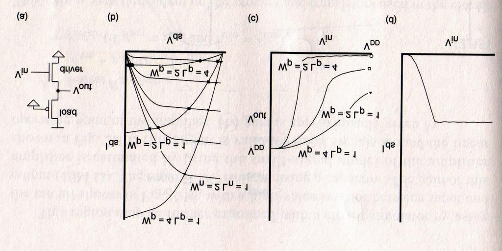
19 .4 Static Load MOS verters Resistor-load verter Current-source-load verter.4.1 Pseudo-NMOS verter Fast (constant current power-consumg P I but speed 19
20 0
21 .6 The Transmission Gate (PMOS (NMOS NMOS pass transistor C load is itially discharged = SS with S=0 ( SS gs = 0 I ds = 0 remas at SS = 5 >, NMOS On = = gs t 0 S=1 ( dd gs = (itially 5 > charge gs = t >, current from to As the put voltage approaches, the n-device begs to turn off tn 1
22 S=0 (open circuit, remas at tn ( dd, where tn ( dd denotes the t at = (body effect s dd S=1 = 0 = tn ( dd n-device beg to conduct, and fall to ss Transmission of Logic 1 is degraded, ( tn Transmission of Logic 0 is not degraded, ( ss PMOS pass transistor S=1,(S=0 (open = ss = ss S=0 (close =, current to charge (C_load
23 S=0 (close = ss, = Discharge C_load until through p-device conductg until =, at which pot the transistor stops tp ( ss p-mos passes good 1 p-mos passes poor 0 Transmission gate can pass logic 1 and 0 with degradation! overall behavior (1 S=0 ( S = 1 : N,P devices are OFF = SS, = Z (high impedance =, = Z ( S=1 ( S = 0 : N,P devices are ON = SS, SS =, =, = Used multiplexg element & latch element act as voltage-controlled resistor connectg the put and put Example to analyze a CMOS circuit Way 1=MAN Way =SPICE 3
24 (1 Capacitor loaded circuit Cload at ss * Cload is large When S is ON NMOS, S = 0 1 PMOS, S = 1 0 Results: Currents of the pass transistor are monitored (transmission gate, gs ( p = 5 (constant current (PMOS It starts at saturation (transmission gate as nonsaturation > gsp tp dsp (NMOS always at saturation, = dsn gsn Rise < gsn tn dsn After, NMOS is off tn 4
25 Three regions of operation : A N saturation P saturation < tp B N saturation P nonsaturation tp < < tn C N off P nonsaturation tn < a. Region A p : constant current source n : current varies versely with b. Region B both currents vary learly (verse with c. Region C p-current varies verse learly with Charge current amount 5
26 check : =, SS = SS ( Lightly loaded circuit (Cload is small follows very closely Fig.35(d n-current for = 0. 1 p-current Three regions of operation : a. n (lear, p (off b. n (lear, p (lear c. n (off, p (lear SPICE can be monitored by usg Combed 6
MOS Transistor Theory
 CHAPTER 3 MOS Transistor Theory Outline 2 1. Introduction 2. Ideal I-V Characteristics 3. Nonideal I-V Effects 4. C-V Characteristics 5. DC Transfer Characteristics 6. Switch-level RC Delay Models MOS
MOS Transistor Theory
 MOS Transistor Theory So far, we have viewed a MOS transistor as an ideal switch (digital operation) Reality: less than ideal EE 261 Krish Chakrabarty 1 Introduction So far, we have treated transistors
MOS Transistor Theory MOSFET Symbols Current Characteristics of MOSFET. MOS Symbols and Characteristics. nmos Enhancement Transistor
 MOS Transistor Theory MOSFET Symbols Current Characteristics of MOSFET Calculation of t and Important 2 nd Order Effects SmallSignal Signal MOSFET Model Summary Material from: CMOS LSI Design By Weste
MOSFET: Introduction
 E&CE 437 Integrated VLSI Systems MOS Transistor 1 of 30 MOSFET: Introduction Metal oxide semiconductor field effect transistor (MOSFET) or MOS is widely used for implementing digital designs Its major
Chapter 2 CMOS Transistor Theory. Jin-Fu Li Department of Electrical Engineering National Central University Jungli, Taiwan
 Chapter 2 CMOS Transistor Theory Jin-Fu Li Department of Electrical Engineering National Central University Jungli, Taiwan Outline Introduction MOS Device Design Equation Pass Transistor Jin-Fu Li, EE,
ECE 546 Lecture 10 MOS Transistors
 ECE 546 Lecture 10 MOS Transistors Spring 2018 Jose E. Schutt-Aine Electrical & Computer Engineering University of Illinois jesa@illinois.edu NMOS Transistor NMOS Transistor N-Channel MOSFET Built on p-type
Chapter 4 Field-Effect Transistors
 Chapter 4 Field-Effect Transistors Microelectronic Circuit Design Richard C. Jaeger Travis N. Blalock 5/5/11 Chap 4-1 Chapter Goals Describe operation of MOSFETs. Define FET characteristics in operation
DC and Transient Responses (i.e. delay) (some comments on power too!)
 (some comments on power too!)") DC and Transient Responses (i.e. delay) (some comments on power too!) Michael Niemier (Some slides based on lecture notes by David Harris) 1 Lecture 02 - CMOS Transistor Theory & the Effects of Scaling
DC and Transient Responses (i.e. delay) (some comments on power too!) Michael Niemier (Some slides based on lecture notes by David Harris) 1 Lecture 02 - CMOS Transistor Theory & the Effects of Scaling
MOS Transistor I-V Characteristics and Parasitics
 ECEN454 Digital Integrated Circuit Design MOS Transistor I-V Characteristics and Parasitics ECEN 454 Facts about Transistors So far, we have treated transistors as ideal switches An ON transistor passes
Lecture 5: CMOS Transistor Theory
 Lecture 5: CMOS Transistor Theory Slides courtesy of Deming Chen Slides based on the initial set from David Harris CMOS VLSI Design Outline q q q q q q q Introduction MOS Capacitor nmos I-V Characteristics
The Devices. Jan M. Rabaey
 The Devices Jan M. Rabaey Goal of this chapter Present intuitive understanding of device operation Introduction of basic device equations Introduction of models for manual analysis Introduction of models
Lecture 12 Digital Circuits (II) MOS INVERTER CIRCUITS
 MOS INVERTER CIRCUITS") Lecture 12 Digital Circuits (II) MOS INVERTER CIRCUITS Outline NMOS inverter with resistor pull-up The inverter NMOS inverter with current-source pull-up Complementary MOS (CMOS) inverter Static analysis
Lecture 12 Digital Circuits (II) MOS INVERTER CIRCUITS Outline NMOS inverter with resistor pull-up The inverter NMOS inverter with current-source pull-up Complementary MOS (CMOS) inverter Static analysis
The Devices. Devices
 The The MOS Transistor Gate Oxyde Gate Source n+ Polysilicon Drain n+ Field-Oxyde (SiO 2 ) p-substrate p+ stopper Bulk Contact CROSS-SECTION of NMOS Transistor Cross-Section of CMOS Technology MOS transistors
Microelectronics Part 1: Main CMOS circuits design rules
 GBM8320 Dispositifs Médicaux telligents Microelectronics Part 1: Main CMOS circuits design rules Mohamad Sawan et al. Laboratoire de neurotechnologies Polystim! http://www.cours.polymtl.ca/gbm8320/! med-amine.miled@polymtl.ca!
University of Pennsylvania Department of Electrical Engineering. ESE 570 Midterm Exam March 14, 2013 FORMULAS AND DATA
 University of Pennsylvania Department of Electrical Engineering ESE 570 Midterm Exam March 4, 03 FORMULAS AND DATA. PHYSICAL CONSTANTS: n i = intrinsic concentration undoped) silicon =.45 x 0 0 cm -3 @
EE 560 MOS TRANSISTOR THEORY
 1 EE 560 MOS TRANSISTOR THEORY PART 1 TWO TERMINAL MOS STRUCTURE V G (GATE VOLTAGE) 2 GATE OXIDE SiO 2 SUBSTRATE p-type doped Si (N A = 10 15 to 10 16 cm -3 ) t ox V B (SUBSTRATE VOLTAGE) EQUILIBRIUM:
Lecture 3: CMOS Transistor Theory
 Lecture 3: CMOS Transistor Theory Outline Introduction MOS Capacitor nmos I-V Characteristics pmos I-V Characteristics Gate and Diffusion Capacitance 2 Introduction So far, we have treated transistors
The Devices: MOS Transistors
 The Devices: MOS Transistors References: Semiconductor Device Fundamentals, R. F. Pierret, Addison-Wesley Digital Integrated Circuits: A Design Perspective, J. Rabaey et.al. Prentice Hall NMOS Transistor
Fig. 1 CMOS Transistor Circuits (a) Inverter Out = NOT In, (b) NOR-gate C = NOT (A or B)
 Inverter Out = NOT In, (b) NOR-gate C = NOT (A or B)") 1 Introduction to Transistor-Level Logic Circuits 1 By Prawat Nagvajara At the transistor level of logic circuits, transistors operate as switches with the logic variables controlling the open or closed
1 Introduction to Transistor-Level Logic Circuits 1 By Prawat Nagvajara At the transistor level of logic circuits, transistors operate as switches with the logic variables controlling the open or closed
CMPEN 411 VLSI Digital Circuits. Lecture 04: CMOS Inverter (static view)
") CMPEN 411 VLSI Digital Circuits Lecture 04: CMOS Inverter (static view) Kyusun Choi [Adapted from Rabaey s Digital Integrated Circuits, Second Edition, 2003 J. Rabaey, A. Chandrakasan, B. Nikolic] CMPEN
CMPEN 411 VLSI Digital Circuits Lecture 04: CMOS Inverter (static view) Kyusun Choi [Adapted from Rabaey s Digital Integrated Circuits, Second Edition, 2003 J. Rabaey, A. Chandrakasan, B. Nikolic] CMPEN
Lecture 12: MOS Capacitors, transistors. Context
 Lecture 12: MOS Capacitors, transistors Context In the last lecture, we discussed PN diodes, and the depletion layer into semiconductor surfaces. Small signal models In this lecture, we will apply those
The Devices. Digital Integrated Circuits A Design Perspective. Jan M. Rabaey Anantha Chandrakasan Borivoje Nikolic. July 30, 2002
 Digital Integrated Circuits A Design Perspective Jan M. Rabaey Anantha Chandrakasan Borivoje Nikolic The Devices July 30, 2002 Goal of this chapter Present intuitive understanding of device operation Introduction
Lecture 4: CMOS Transistor Theory
 Introduction to CMOS VLSI Design Lecture 4: CMOS Transistor Theory David Harris, Harvey Mudd College Kartik Mohanram and Steven Levitan University of Pittsburgh Outline q Introduction q MOS Capacitor q
EEC 118 Lecture #2: MOSFET Structure and Basic Operation. Rajeevan Amirtharajah University of California, Davis Jeff Parkhurst Intel Corporation
 EEC 118 Lecture #2: MOSFET Structure and Basic Operation Rajeevan Amirtharajah University of California, Davis Jeff Parkhurst Intel Corporation Announcements Lab 1 this week, report due next week Bring
II III IV V VI B C N. Al Si P S. Zn Ga Ge As Se Cd In Sn Sb Te. Silicon (Si) the dominating material in IC manufacturing
 the dominating material in IC manufacturing") II III IV V VI B N Al Si P S Zn Ga Ge As Se d In Sn Sb Te Silicon (Si) the dominating material in I manufacturing ompound semiconductors III - V group: GaAs GaN GaSb GaP InAs InP InSb... The Energy Band
II III IV V VI B N Al Si P S Zn Ga Ge As Se d In Sn Sb Te Silicon (Si) the dominating material in I manufacturing ompound semiconductors III - V group: GaAs GaN GaSb GaP InAs InP InSb... The Energy Band
FIELD-EFFECT TRANSISTORS
 FIEL-EFFECT TRANSISTORS 1 Semiconductor review 2 The MOS capacitor 2 The enhancement-type N-MOS transistor 3 I-V characteristics of enhancement MOSFETS 4 The output characteristic of the MOSFET in saturation
ECE 342 Electronic Circuits. Lecture 6 MOS Transistors
 ECE 342 Electronic Circuits Lecture 6 MOS Transistors Jose E. Schutt-Aine Electrical & Computer Engineering University of Illinois jesa@illinois.edu 1 NMOS Transistor Typically L = 0.1 to 3 m, W = 0.2
ESE 570: Digital Integrated Circuits and VLSI Fundamentals
 ESE 570: Digital Integrated Circuits and VLSI Fundamentals Lec 4: January 23, 2018 MOS Transistor Theory, MOS Model Penn ESE 570 Spring 2018 Khanna Lecture Outline! CMOS Process Enhancements! Semiconductor
DC & Transient Responses
 ECEN454 Digital Integrated Circuit Design DC & Transient Responses ECEN 454 DC Response DC Response: vs. for a gate Ex: Inverter When = -> = When = -> = In between, depends on transistor size and current
The Physical Structure (NMOS)
") The Physical Structure (NMOS) Al SiO2 Field Oxide Gate oxide S n+ Polysilicon Gate Al SiO2 SiO2 D n+ L channel P Substrate Field Oxide contact Metal (S) n+ (G) L W n+ (D) Poly 1 Transistor Resistance Two
The Physical Structure (NMOS) Al SiO2 Field Oxide Gate oxide S n+ Polysilicon Gate Al SiO2 SiO2 D n+ L channel P Substrate Field Oxide contact Metal (S) n+ (G) L W n+ (D) Poly 1 Transistor Resistance Two
EE105 Fall 2014 Microelectronic Devices and Circuits. NMOS Transistor Capacitances: Saturation Region
 EE105 Fall 014 Microelectronic Devices and Circuits Prof. Ming C. Wu wu@eecs.berkeley.edu 511 Sutardja Dai Hall (SDH) 1 NMOS Transistor Capacitances: Saturation Region Drain no longer connected to channel
VLSI Design The MOS Transistor
 VLSI Design The MOS Transistor Frank Sill Torres Universidade Federal de Minas Gerais (UFMG), Brazil VLSI Design: CMOS Technology 1 Outline Introduction MOS Capacitor nmos I-V Characteristics pmos I-V
ECE 342 Electronic Circuits. 3. MOS Transistors
 ECE 342 Electronic Circuits 3. MOS Transistors Jose E. Schutt-Aine Electrical & Computer Engineering University of Illinois jschutt@emlab.uiuc.edu 1 NMOS Transistor Typically L = 0.1 to 3 m, W = 0.2 to
Digital Integrated Circuits A Design Perspective. Jan M. Rabaey Anantha Chandrakasan Borivoje Nikolic. The Devices. July 30, Devices.
 Digital Integrated Circuits A Design Perspective Jan M. Rabaey Anantha Chandrakasan Borivoje Nikolic The July 30, 2002 1 Goal of this chapter Present intuitive understanding of device operation Introduction
Practice 3: Semiconductors
 Practice 3: Semiconductors Digital Electronic Circuits Semester A 2012 VLSI Fabrication Process VLSI Very Large Scale Integration The ability to fabricate many devices on a single substrate within a given
CMPEN 411 VLSI Digital Circuits. Lecture 03: MOS Transistor
 CMPEN 411 VLSI Digital Circuits Lecture 03: MOS Transistor Kyusun Choi [Adapted from Rabaey s Digital Integrated Circuits, Second Edition, 2003 J. Rabaey, A. Chandrakasan, B. Nikolic] CMPEN 411 L03 S.1
CMOS INVERTER. Last Lecture. Metrics for qualifying digital circuits. »Cost» Reliability» Speed (delay)»performance
»performance") CMOS INVERTER Last Lecture Metrics for qualifying digital circuits»cost» Reliability» Speed (delay)»performance 1 Today s lecture The CMOS inverter at a glance An MOS transistor model for manual analysis
CMOS INVERTER Last Lecture Metrics for qualifying digital circuits»cost» Reliability» Speed (delay)»performance 1 Today s lecture The CMOS inverter at a glance An MOS transistor model for manual analysis
Lecture 11: MOS Transistor
 Lecture 11: MOS Transistor Prof. Niknejad Lecture Outline Review: MOS Capacitors Regions MOS Capacitors (3.8 3.9) CV Curve Threshold Voltage MOS Transistors (4.1 4.3): Overview Cross-section and layout
ENGR890 Digital VLSI Design Fall Lecture 4: CMOS Inverter (static view)
") ENGR89 Digital VLSI Design Fall 5 Lecture 4: CMOS Inverter (static view) [Adapted from Chapter 5 of Digital Integrated Circuits, 3, J. Rabaey et al.] [Also borrowed from Vijay Narayanan and Mary Jane Irwin]
ENGR89 Digital VLSI Design Fall 5 Lecture 4: CMOS Inverter (static view) [Adapted from Chapter 5 of Digital Integrated Circuits, 3, J. Rabaey et al.] [Also borrowed from Vijay Narayanan and Mary Jane Irwin]
ECEN474/704: (Analog) VLSI Circuit Design Spring 2018
 VLSI Circuit Design Spring 2018") ECEN474/704: (Analog) SI Circuit Design Spring 2018 ecture 2: MOS ransistor Modeling Sam Palermo Analog & Mixed-Signal Center exas A&M University Announcements If you haven t already, turn in your 0.18um
ECEN474/704: (Analog) SI Circuit Design Spring 2018 ecture 2: MOS ransistor Modeling Sam Palermo Analog & Mixed-Signal Center exas A&M University Announcements If you haven t already, turn in your 0.18um
Integrated Circuits & Systems
 Federal University of Santa Catarina Center for Technology Computer Science & Electronics Engineering Integrated Circuits & Systems INE 5442 Lecture 10 MOSFET part 1 guntzel@inf.ufsc.br ual-well Trench-Isolated
ESE 570: Digital Integrated Circuits and VLSI Fundamentals
 ESE 570: Digital Integrated Circuits and VLSI Fundamentals Lec 4: January 29, 2019 MOS Transistor Theory, MOS Model Penn ESE 570 Spring 2019 Khanna Lecture Outline! CMOS Process Enhancements! Semiconductor
MOS Transistors. Prof. Krishna Saraswat. Department of Electrical Engineering Stanford University Stanford, CA
 MOS Transistors Prof. Krishna Saraswat Department of Electrical Engineering S Stanford, CA 94305 saraswat@stanford.edu 1 1930: Patent on the Field-Effect Transistor! Julius Lilienfeld filed a patent describing
VLSI Design and Simulation
 VLSI Design and Simulation CMOS Inverters Topics Inverter VTC Noise Margin Static Load Inverters CMOS Inverter First-Order DC Analysis R p V OL = 0 V OH = R n =0 = CMOS Inverter: Transient Response R p
EE105 - Fall 2006 Microelectronic Devices and Circuits
 EE105 - Fall 2006 Microelectronic Devices and Circuits Prof. Jan M. Rabaey (jan@eecs) Lecture 7: MOS Transistor Some Administrative Issues Lab 2 this week Hw 2 due on We Hw 3 will be posted same day MIDTERM
MOS Transistor Properties Review
 MOS Transistor Properties Review 1 VLSI Chip Manufacturing Process Photolithography: transfer of mask patterns to the chip Diffusion or ion implantation: selective doping of Si substrate Oxidation: SiO
CS/EE N-type Transistor
 CS/EE 6710 MOS Transistor Models Electrical Effects Propagation Delay N-type Transistor D + G Vds i electrons +Vgs S - 1 Another Cutaway View Thanks to National Central University for Some images Vgs Forms
! CMOS Process Enhancements. ! Semiconductor Physics. " Band gaps. " Field Effects. ! MOS Physics. " Cut-off. " Depletion.
 ESE 570: Digital Integrated Circuits and VLSI Fundamentals Lec 4: January 3, 018 MOS Transistor Theory, MOS Model Lecture Outline! CMOS Process Enhancements! Semiconductor Physics " Band gaps " Field Effects!
ESE 570: Digital Integrated Circuits and VLSI Fundamentals
 ESE 570: Digital Integrated Circuits and VLSI Fundamentals Lec 4: January 24, 2017 MOS Transistor Theory, MOS Model Penn ESE 570 Spring 2017 Khanna Lecture Outline! Semiconductor Physics " Band gaps "
CHAPTER 5 MOS FIELD-EFFECT TRANSISTORS
 CHAPTER 5 MOS FIELD-EFFECT TRANSISTORS 5.1 The MOS capacitor 5.2 The enhancement-type N-MOS transistor 5.3 I-V characteristics of enhancement mode MOSFETS 5.4 The PMOS transistor and CMOS technology 5.5
Introduction to CMOS VLSI. Chapter 2: CMOS Transistor Theory. Harris, 2004 Updated by Li Chen, Outline
 Introduction to MOS VLSI Design hapter : MOS Transistor Theory copyright@david Harris, 004 Updated by Li hen, 010 Outline Introduction MOS apacitor nmos IV haracteristics pmos IV haracteristics Gate and
Device Models (PN Diode, MOSFET )
") Device Models (PN Diode, MOSFET ) Instructor: Steven P. Levitan steve@ece.pitt.edu TA: Gayatri Mehta, José Martínez Book: Digital Integrated Circuits: A Design Perspective; Jan Rabaey Lab Notes: Handed
Device Models (PN Diode, MOSFET ) Instructor: Steven P. Levitan steve@ece.pitt.edu TA: Gayatri Mehta, José Martínez Book: Digital Integrated Circuits: A Design Perspective; Jan Rabaey Lab Notes: Handed
EEC 116 Lecture #3: CMOS Inverters MOS Scaling. Rajeevan Amirtharajah University of California, Davis Jeff Parkhurst Intel Corporation
 EEC 116 Lecture #3: CMOS Inverters MOS Scaling Rajeevan Amirtharajah University of California, Davis Jeff Parhurst Intel Corporation Outline Review: Inverter Transfer Characteristics Lecture 3: Noise Margins,
Lecture 12 Circuits numériques (II)
") Lecture 12 Circuits numériques (II) Circuits inverseurs MOS Outline NMOS inverter with resistor pull-up The inverter NMOS inverter with current-source pull-up Complementary MOS (CMOS) inverter Static analysis
Lecture 12 Circuits numériques (II) Circuits inverseurs MOS Outline NMOS inverter with resistor pull-up The inverter NMOS inverter with current-source pull-up Complementary MOS (CMOS) inverter Static analysis
Quantitative MOSFET. Step 1. Connect the MOS capacitor results for the electron charge in the inversion layer Q N to the drain current.
 Quantitative MOSFET Step 1. Connect the MOS capacitor results for the electron charge in the inversion layer Q N to the drain current. V DS _ n source polysilicon gate y = y * 0 x metal interconnect to
MOS Inverters. Digital Electronics - INEL Prof. Manuel Jiménez. With contributions by: Rafael A. Arce Nazario
 MOS Inverters igital Electronics - INE 407 Prof. Manuel Jiménez With contributions by: Rafael A. Arce Nazario Objectives: Introduce MOS Inverter Styles Resistor oad Enhancement oad Saturated / ear epletion
The Intrinsic Silicon
 The Intrinsic ilicon Thermally generated electrons and holes Carrier concentration p i =n i ni=1.45x10 10 cm-3 @ room temp Generally: n i = 3.1X10 16 T 3/2 e -1.21/2KT cm -3 T= temperature in K o (egrees
EE105 - Fall 2005 Microelectronic Devices and Circuits
 EE105 - Fall 005 Microelectronic Devices and Circuits ecture 7 MOS Transistor Announcements Homework 3, due today Homework 4 due next week ab this week Reading: Chapter 4 1 ecture Material ast lecture
Lecture 15 OUTLINE. MOSFET structure & operation (qualitative) Review of electrostatics The (N)MOS capacitor
 Review of electrostatics The (N)MOS capacitor") Lecture 15 OUTLINE MOSFET structure & operation (qualitative) Review of electrostatics The (N)MOS capacitor Electrostatics t ti Charge vs. voltage characteristic Reading: Chapter 6.1 6.2.1 EE105 Fall 2007
Lecture 15 OUTLINE MOSFET structure & operation (qualitative) Review of electrostatics The (N)MOS capacitor Electrostatics t ti Charge vs. voltage characteristic Reading: Chapter 6.1 6.2.1 EE105 Fall 2007
Lecture 15 OUTLINE. MOSFET structure & operation (qualitative) Review of electrostatics The (N)MOS capacitor
 Review of electrostatics The (N)MOS capacitor") Lecture 15 OUTLINE MOSFET structure & operation (qualitative) Review of electrostatics The (N)MOS capacitor Electrostatics Charge vs. voltage characteristic Reading: Chapter 6.1 6.2.1 EE15 Spring 28 Lecture
Lecture 15 OUTLINE MOSFET structure & operation (qualitative) Review of electrostatics The (N)MOS capacitor Electrostatics Charge vs. voltage characteristic Reading: Chapter 6.1 6.2.1 EE15 Spring 28 Lecture
! CMOS Process Enhancements. ! Semiconductor Physics. " Band gaps. " Field Effects. ! MOS Physics. " Cut-off. " Depletion.
 ESE 570: Digital Integrated Circuits and VLSI Fundamentals Lec 4: January 9, 019 MOS Transistor Theory, MOS Model Lecture Outline CMOS Process Enhancements Semiconductor Physics Band gaps Field Effects
Content. MIS Capacitor. Accumulation Depletion Inversion MOS CAPACITOR. A Cantoni Digital Switching
 Content MIS Capacitor Accumulation Depletion Inversion MOS CAPACITOR 1 MIS Capacitor Metal Oxide C ox p-si C s Components of a capacitance model for the MIS structure 2 MIS Capacitor- Accumulation ρ( x)
Device Models (PN Diode, MOSFET )
") Device Models (PN Diode, MOSFET ) Instructor: Steven P. Levitan steve@ece.pitt.edu TA: Gayatri Mehta, José Martínez Book: Digital Integrated Circuits: A Design Perspective; Jan Rabaey Lab Notes: Handed
Device Models (PN Diode, MOSFET ) Instructor: Steven P. Levitan steve@ece.pitt.edu TA: Gayatri Mehta, José Martínez Book: Digital Integrated Circuits: A Design Perspective; Jan Rabaey Lab Notes: Handed
CMOS Inverter (static view)
") Review: Design Abstraction Levels SYSTEM CMOS Inverter (static view) + MODULE GATE [Adapted from Chapter 5. 5.3 CIRCUIT of G DEVICE Rabaey s Digital Integrated Circuits,, J. Rabaey et al.] S D Review:
Review: Design Abstraction Levels SYSTEM CMOS Inverter (static view) + MODULE GATE [Adapted from Chapter 5. 5.3 CIRCUIT of G DEVICE Rabaey s Digital Integrated Circuits,, J. Rabaey et al.] S D Review:
The Devices. Digital Integrated Circuits A Design Perspective. Jan M. Rabaey Anantha Chandrakasan Borivoje Nikolic. July 30, 2002
 igital Integrated Circuits A esign Perspective Jan M. Rabaey Anantha Chandrakasan Borivoje Nikolic The evices July 30, 2002 Goal of this chapter Present intuitive understanding of device operation Introduction
Charge Storage in the MOS Structure. The Inverted MOS Capacitor (V GB > V Tn )
") The Inverted MO Capacitor (V > V Tn ) We consider the surface potential as Þxed (ÒpinnedÓ) at φ s,max = - φ p φ(x).5 V. V V ox Charge torage in the MO tructure Three regions of operation: Accumulation:
The Inverted MO Capacitor (V > V Tn ) We consider the surface potential as Þxed (ÒpinnedÓ) at φ s,max = - φ p φ(x).5 V. V V ox Charge torage in the MO tructure Three regions of operation: Accumulation:
SECTION: Circle one: Alam Lundstrom. ECE 305 Exam 5 SOLUTIONS: Spring 2016 April 18, 2016 M. A. Alam and M.S. Lundstrom Purdue University
 NAME: PUID: SECTION: Circle one: Alam Lundstrom ECE 305 Exam 5 SOLUTIONS: April 18, 2016 M A Alam and MS Lundstrom Purdue University This is a closed book exam You may use a calculator and the formula
Operation and Modeling of. The MOS Transistor. Second Edition. Yannis Tsividis Columbia University. New York Oxford OXFORD UNIVERSITY PRESS
 Operation and Modeling of The MOS Transistor Second Edition Yannis Tsividis Columbia University New York Oxford OXFORD UNIVERSITY PRESS CONTENTS Chapter 1 l.l 1.2 1.3 1.4 1.5 1.6 1.7 Chapter 2 2.1 2.2
Section 12: Intro to Devices
 Section 12: Intro to Devices Extensive reading materials on reserve, including Robert F. Pierret, Semiconductor Device Fundamentals EE143 Ali Javey Bond Model of Electrons and Holes Si Si Si Si Si Si Si
Today s lecture. EE141- Spring 2003 Lecture 4. Design Rules CMOS Inverter MOS Transistor Model
 - Spring 003 Lecture 4 Design Rules CMOS Inverter MOS Transistor Model Today s lecture Design Rules The CMOS inverter at a glance An MOS transistor model for manual analysis Important! Labs start next
ECE-305: Fall 2017 MOS Capacitors and Transistors
 ECE-305: Fall 2017 MOS Capacitors and Transistors Pierret, Semiconductor Device Fundamentals (SDF) Chapters 15+16 (pp. 525-530, 563-599) Professor Peter Bermel Electrical and Computer Engineering Purdue
LECTURE 3 MOSFETS II. MOS SCALING What is Scaling?
 LECTURE 3 MOSFETS II Lecture 3 Goals* * Understand constant field and constant voltage scaling and their effects. Understand small geometry effects for MOS transistors and their implications modeling and
ECE 438: Digital Integrated Circuits Assignment #4 Solution The Inverter
 ECE 438: Digital Integrated Circuits Assignment #4 The Inverter Text: Chapter 5, Digital Integrated Circuits 2 nd Ed, Rabaey 1) Consider the CMOS inverter circuit in Figure P1 with the following parameters.
ESE 570: Digital Integrated Circuits and VLSI Fundamentals
 ESE 570: Digital Integrated Circuits and VLSI Fundamentals Lec 5: January 25, 2018 MOS Operating Regions, pt. 1 Lecture Outline! 3 Regions of operation for MOSFET " Subthreshold " Linear " Saturation!
Semiconductor Physics Problems 2015
 Semiconductor Physics Problems 2015 Page and figure numbers refer to Semiconductor Devices Physics and Technology, 3rd edition, by SM Sze and M-K Lee 1. The purest semiconductor crystals it is possible
Lecture 5: DC & Transient Response
 Lecture 5: DC & Transient Response Outline q Pass Transistors q DC Response q Logic Levels and Noise Margins q Transient Response q RC Delay Models q Delay Estimation 2 Activity 1) If the width of a transistor
6.012 Electronic Devices and Circuits
 Page 1 of 10 YOUR NAME Department of Electrical Engineering and Computer Science Massachusetts Institute of Technology 6.012 Electronic Devices and Circuits Exam No. 2 Thursday, November 5, 2009 7:30 to
Lecture 14 - Digital Circuits (III) CMOS. April 1, 2003
 CMOS. April 1, 2003") 6.12 - Microelectronic Devices and Circuits - Spring 23 Lecture 14-1 Lecture 14 - Digital Circuits (III) CMOS April 1, 23 Contents: 1. Complementary MOS (CMOS) inverter: introduction 2. CMOS inverter:
6.12 - Microelectronic Devices and Circuits - Spring 23 Lecture 14-1 Lecture 14 - Digital Circuits (III) CMOS April 1, 23 Contents: 1. Complementary MOS (CMOS) inverter: introduction 2. CMOS inverter:
EE115C Winter 2017 Digital Electronic Circuits. Lecture 3: MOS RC Model, CMOS Manufacturing
 EE115C Winter 2017 Digital Electronic Circuits Lecture 3: MOS RC Model, CMOS Manufacturing Agenda MOS Transistor: RC Model (pp. 104-113) S R on D CMOS Manufacturing Process (pp. 36-46) S S C GS G G C GD
Lecture 12: MOSFET Devices
 Lecture 12: MOSFET Devices Gu-Yeon Wei Division of Engineering and Applied Sciences Harvard University guyeon@eecs.harvard.edu Wei 1 Overview Reading S&S: Chapter 5.1~5.4 Supplemental Reading Background
Lecture 15: MOS Transistor models: Body effects, SPICE models. Context. In the last lecture, we discussed the modes of operation of a MOS FET:
 Lecture 15: MOS Transistor models: Body effects, SPICE models Context In the last lecture, we discussed the modes of operation of a MOS FET: oltage controlled resistor model I- curve (Square-Law Model)
Lecture 11 VTCs and Delay. No lab today, Mon., Tues. Labs restart next week. Midterm #1 Tues. Oct. 7 th, 6:30-8:00pm in 105 Northgate
 EE4-Fall 2008 Digital Integrated Circuits Lecture VTCs and Delay Lecture # Announcements No lab today, Mon., Tues. Labs restart next week Midterm # Tues. Oct. 7 th, 6:30-8:00pm in 05 Northgate Exam is
Semiconductor Physics fall 2012 problems
 Semiconductor Physics fall 2012 problems 1. An n-type sample of silicon has a uniform density N D = 10 16 atoms cm -3 of arsenic, and a p-type silicon sample has N A = 10 15 atoms cm -3 of boron. For each
EEE 421 VLSI Circuits
 EEE 421 CMOS Properties Full rail-to-rail swing high noise margins» Logic levels not dependent upon the relative device sizes transistors can be minimum size ratioless Always a path to V dd or GND in steady
Lecture Outline. ESE 570: Digital Integrated Circuits and VLSI Fundamentals. Review: MOSFET N-Type, P-Type. Semiconductor Physics.
 ESE 57: Digital Integrated Circuits and VLSI Fundamentals Lec 4: January 24, 217 MOS Transistor Theory, MOS Model Lecture Outline! Semiconductor Physics " Band gaps " Field Effects! MOS Physics " Cutoff
6.012 Electronic Devices and Circuits Spring 2005
 6.012 Electronic Devices and Circuits Spring 2005 May 16, 2005 Final Exam (200 points) -OPEN BOOK- Problem NAME RECITATION TIME 1 2 3 4 5 Total General guidelines (please read carefully before starting):
2007 Fall: Electronic Circuits 2 CHAPTER 10. Deog-Kyoon Jeong School of Electrical Engineering
 007 Fall: Electronic Circuits CHAPTER 10 Digital CMOS Logic Circuits Deog-Kyoon Jeong dkjeong@snu.ac.kr k School of Electrical Engineering Seoul lnational luniversity it Introduction In this chapter, we
EE 560 MOS TRANSISTOR THEORY PART 2. Kenneth R. Laker, University of Pennsylvania
 1 EE 560 MOS TRANSISTOR THEORY PART nmos TRANSISTOR IN LINEAR REGION V S = 0 V G > V T0 channel SiO V D = small 4 C GC C BC substrate depletion region or bulk B p nmos TRANSISTOR AT EDGE OF SATURATION
Digital Integrated Circuits
 Chapter 6 The CMOS Inverter 1 Contents Introduction (MOST models) 0, 1 st, 2 nd order The CMOS inverter : The static behavior: o DC transfer characteristics, o Short-circuit current The CMOS inverter :
Lecture 6: DC & Transient Response
 Lecture 6: DC & Transient Response Slides courtesy of Deming Chen Slides based on the initial set from David Harris CMOS VLSI Design Outline Pass Transistors DC Response Logic Levels and Noise Margins
Circuits. L2: MOS Models-2 (1 st Aug. 2013) B. Mazhari Dept. of EE, IIT Kanpur. B. Mazhari, IITK. G-Number
 B. Mazhari Dept. of EE, IIT Kanpur. B. Mazhari, IITK. G-Number") EE610: CMOS Analog Circuits L: MOS Models- (1 st Aug. 013) B. Mazhari Dept. of EE, IIT Kanpur 3 NMOS Models MOS MODEL Above Threshold Subthreshold ( GS > TN ) ( GS < TN ) Saturation ti Ti Triode ( DS >
EE610: CMOS Analog Circuits L: MOS Models- (1 st Aug. 013) B. Mazhari Dept. of EE, IIT Kanpur 3 NMOS Models MOS MODEL Above Threshold Subthreshold ( GS > TN ) ( GS < TN ) Saturation ti Ti Triode ( DS >
1. The MOS Transistor. Electrical Conduction in Solids
 Electrical Conduction in Solids!The band diagram describes the energy levels for electron in solids.!the lower filled band is named Valence Band.!The upper vacant band is named conduction band.!the distance
! MOS Capacitances. " Extrinsic. " Intrinsic. ! Lumped Capacitance Model. ! First Order Capacitor Summary. ! Capacitance Implications
 ESE 570: Digital Integrated Circuits and VLSI Fundamentals Lec 7: February, 07 MOS SPICE Models, MOS Parasitic Details Lecture Outline! MOS Capacitances " Extrinsic " Intrinsic! Lumped Capacitance Model!
THE INVERTER. Inverter
 THE INVERTER DIGITAL GATES Fundamental Parameters Functionality Reliability, Robustness Area Performance» Speed (delay)» Power Consumption» Energy Noise in Digital Integrated Circuits v(t) V DD i(t) (a)
Lecture 6 PN Junction and MOS Electrostatics(III) Metal-Oxide-Semiconductor Structure
 Metal-Oxide-Semiconductor Structure") Lecture 6 PN Junction and MOS Electrostatics(III) Metal-Oxide-Semiconductor Structure Outline 1. Introduction to MOS structure 2. Electrostatics of MOS in thermal equilibrium 3. Electrostatics of MOS with
Lecture 6 PN Junction and MOS Electrostatics(III) Metal-Oxide-Semiconductor Structure Outline 1. Introduction to MOS structure 2. Electrostatics of MOS in thermal equilibrium 3. Electrostatics of MOS with
MOSFET Physics: The Long Channel Approximation
 MOSFET Physics: The ong Channel Approximation A basic n-channel MOSFET (Figure 1) consists of two heavily-doped n-type regions, the Source and Drain, that comprise the main terminals of the device. The
DC and Transient. Courtesy of Dr. Daehyun Dr. Dr. Shmuel and Dr.
 DC and Transient Courtesy of Dr. Daehyun Lim@WSU, Dr. Harris@HMC, Dr. Shmuel Wimer@BIU and Dr. Choi@PSU http://csce.uark.edu +1 (479) 575-604 yrpeng@uark.edu Pass Transistors We have assumed source is
Lecture #27. The Short Channel Effect (SCE)
") Lecture #27 ANNOUNCEMENTS Design Project: Your BJT design should meet the performance specifications to within 10% at both 300K and 360K. ( β dc > 45, f T > 18 GHz, V A > 9 V and V punchthrough > 9 V )
Lecture #27 ANNOUNCEMENTS Design Project: Your BJT design should meet the performance specifications to within 10% at both 300K and 360K. ( β dc > 45, f T > 18 GHz, V A > 9 V and V punchthrough > 9 V )
Lecture 13 - Digital Circuits (II) MOS Inverter Circuits. March 20, 2003
 MOS Inverter Circuits. March 20, 2003") 6.012 Microelectronic Devices and Circuits Spring 2003 Lecture 131 Lecture 13 Digital Circuits (II) MOS Inverter Circuits March 20, 2003 Contents: 1. NMOS inverter with resistor pullup (cont.) 2. NMOS
6.012 Microelectronic Devices and Circuits Spring 2003 Lecture 131 Lecture 13 Digital Circuits (II) MOS Inverter Circuits March 20, 2003 Contents: 1. NMOS inverter with resistor pullup (cont.) 2. NMOS
Lecture 28 Field-Effect Transistors
 Lecture 8 Field-Effect Transistors Field-Effect Transistors 1. Understand MOSFET operation.. Analyze basic FET amplifiers using the loadline technique. 3. Analyze bias circuits. 4. Use small-signal equialent