Section 12: Intro to Devices
|
|
|
- Bruno Norris
- 5 years ago
- Views:
Transcription
1 Section 12: Intro to Devices Extensive reading materials on reserve, including Robert F. Pierret, Semiconductor Device Fundamentals
2 Bond Model of Electrons and Holes Si Si Si Si Si Si Si Si Si Silicon crystal in a two-dimensional representation. Si Si Si Si Si Si Si Si Si Si Si Si Si Si Si Si Si Si When an electron breaks loose and becomes a conduction electron, a hole is also created.
3 Semiconductors, Insulators, and Conductors E c E g1.1 ev E c Ev E g 9 ev E v Top of conduction band empty filled E c Si, Semiconductor SiO 2, insulator Conductor Totally filled bands and totally empty bands do not allow current flow. (Just as there is no motion of liquid in a totally filled or totally empty bottle.) Metal conduction band is half-filled. Semiconductors have lower E G s than insulators and can be doped
4 electron - Bottom of conduction band Intrinsic Carriers Energy gap 1.12 ev hole + Top of valence band n (electron conc) p (hole conc) n i
5 Dopants in Silicon Si Si Si Si Si Si Si As Si Si B Si Si Si Si Si Si Si As, a Group V element, introduces conduction electrons and creates N-type silicon, and is called a donor. B, a Group III element, introduces holes and creates P-type silicon, and is called an acceptor.
6 Types of charges in semiconductors Hole Electron Mobile Charge Carriers they contribute to current flow with electric field is applied. Ionized Donor Ionized Acceptor Immobile Charges they DO NOT contribute to current flow with electric field is applied. However, they affect the local electric field
7 Fermi Function The Probability of an Energy State Being Occupied by an Electron f ( E) ( E E ) / kt E 1+ e 1 f E f is called the Fermi energy or the Fermi level. Boltzmann approximation: f ( E E ) kt f ( E) e E E f >> kt E f E f E f + 3kT + 2kT E f + kt ( E E f ) kt f ( E) e f ( E ) kt E ( E) 1 e f E E f << kt E f E f kt E f 2kT E f 3kT ( E f E ) kt f ( E) 1 e f(e)
8 Electron and Hole Concentrations n N c e ( E E F C ) / kt N c is called the effective density of states. p N v e ( E E V F ) / kt N v is called the effective density of states of the valence band. Remember: the closer E f moves up to E c, the larger n is; the closer E f moves down to E v, the larger p is. For Si, N c cm -3 and N v cm -3.
9 Shifting the Fermi Level
10 Quantitative Relationships n: electron concentration (cm -3 ) p : hole concentration (cm -3 ) N D : donor concentration (cm -3 ) N A : acceptor concentration (cm -3 ) Assume completely ionized to form N D + and N A - 1) Charge neutrality condition: N D + p N A + n 2) Law of Mass Action : n p n i 2 What happens when one doping species dominates?
11 General Effects of Doping on n and p I. N N >> n (i.e., N-type) d a i n N d N a p n 2 i n If N d >> N a, n Nd and p 2 n i N d II. N N >> a d n i (i.e., P-type) p n N a N n 2 i p d If N >>, a N d p Na and n 2 n i N a
12 When an electric field is applied to a semiconductor, mobile carriers will be accelerated by the electrostatic force. This force superimposes on the random thermal motion of carriers: E.g. Electrons drift in the direction opposite to the E-field Current flows E 0 Average drift velocity v μ E 5 1 electron Carrier Drift Carrier mobility 2 E 1 electron
13 Carrier Mobility Mobile carriers are always in random thermal motion. If no electric field is applied, the average current in any direction is zero. Mobility is reduced by 1) collisions with the vibrating atoms phonon scattering 2) deflection by ionized impurity atoms Coulombic scattering - B- - As+ - - Si
14 Total Mobility 1600 Mobility (cm 2 V -1 s -1 ) Electrons Holes 1 τ 1 μ τ 1 + phonon 1 μ phonon + τ 1 impurity 1 μ impurity E14 1E15 1E16 1E17 1E18 1E19 1E20 Total Impurity N Concenration (atoms cm -3 a + N d (cm -3 ) )
15 Conductivity and Resistivity J p,drift qpv qpμ p J n,drift qnv qnμ n J drift J n,drift + J p,drift σ (qnμ n +qpμ p ) conductivity of a semiconductor is σ qnμ n + qpμ p Resistivity, ρ 1/ σ
 ρ")
16 Relationship between Resistivity and Dopant Density DOPANT DENSITY cm -3 N-type P-type RESISTIVITY (Ω cm) ρ 1/σ
17 W I + L V Material with resistivity ρ _ R s Sheet Resistance L t R ρ Wt R s is the resistance when W L ρ t R s value for a given conductive layer (e.g. doped Si, metals) in IC or MEMS technology is used for design and layout of resistors for estimating values of parasitic resistance in a device or circuit R s L W (in ohms/square) if ρ is independent of depth x
18 Diffusion Current Particles diffuse from higher concentration to lower concentration locations.
19 J n, diffusion qd Diffusion Current n dn dx J p, diffusion qd p dp dx D is called the diffusion constant. Signs explained: n p x x
20 Generation/Recombination Processes Recombination continues until excess carriers 0. Time constant of decay is called recombination lifetime
21 Continuity Equations Combining all the carrier actions: n n n n t t + drift t + + diff t thermalr G Now, by the definition of current, we know: n t others n n J J Nx Ny J Nz t + 1 drift t 1 diff q ( x + y + z ) q J Since a change in carrier concentration must occur from a net current Therefore, we can compactly write the continuity equation as: N n t p t 1 q J 1 q N J + P n t thermalr G + + p t thermalr G n t other p t other +
22 PN Junctions Donors N-type P-type I V + I V N P Reverse bias Forward bias diode symbol A PN junction is present in almost every semiconductor device.
23 Energy Band Diagram and Depletion Layer N-region P-region (a) E f E c (b) E c E f E v (c) E v E c E f E v n 0 and p 0 in the depletion layer (d) Neutral N-region Depletion layer Neutral P-region E c E f E v φ bi kt q ln N d 2 i n N a
24 Qualitative Electrostatics Band diagram Built in-potential From ε-dv/dx
25 Depletion-Layer Model Neutral Region N Depletion Layer Neutral Region P On the P-side of the depletion layer, ρ qn a x 0 n x p ρ d dx qn a ε s x n qn d qn a x p x qna qna ( x) x + C 1 ( x p x) ε ε s s E On the N-side, ρ qn d x x n 0 p x qnd ( x ) ( x + xn ) ε s
26 Effect of Bias on Electrostatics
27 Current Flow - Qualitative
28 PN Diode IV Characteristics I qv kt I0( e 1) I 0 Aqn 2 i L D p p N d + Dn L N n a I I + r 0 A qnw i τ dep dep
29 MOS Capacitors MOS: Metal-Oxide-Semiconductor V g metal gate V g gate SiO 2 N + SiO 2 N + Si body P-body MOS capacitor MOS transistor
30 MOS Band Diagram
31 Flat-band Condition and Flat-band Voltage χ SiO ev E c E 0 qψ M 3.1 ev 3.1 ev χ Si qψ s χ Si + (E c E f ) 4.05eV E c, E f E c V fb E v N + -poly-si 9 ev P-body E f E v E 0 : Vacuum level E 0 E f : Work function E 0 E c : Electron affinity Si/SiO 2 energy barrier E v 4.8 ev Vfb ψ ψ M s SiO 2
32 Biasing Conditions
33 Biasing Conditions (2)
34 E c, E f E v qv g Depletion and the Depletion Width qv ox qφ s W de p depletion region M O S E c E fev The charge within the depletion region is: ρ qn A Poisson s equation reduces to: dε ρ qn A K0 x W dx ε ε Si Integrating twice gives: φ S qn 2ε A Si Si W 2 (b) Or: W 2ε Si qn φ A S
35 Surface Depletion V V g > V fb gate depletion layer charge, Q dep P-Si body SiO 2 E c, E f E v qv g qv ox qφ s W de p depletion region E c E fev V ox Q C V g s ox V Q (a) C fb + φ + V s dep ox ox qn a C ox V W fb dep + φ + s qn a C qn M O S 2ε φ ox a s C 2ε φ ox s s s (b)
36 Threshold Condition and Threshold Voltage threshold of inversion E c φ st threshold : n s N a A C qφ Β E i (E c E f ) surface (E f E v ) bulk qv g qv t D B E f E v AB, and C D E c, E f φ st 2φ B kt 2 ln q N n i a E v M O S qφ B E 2 g ( E f E v ) bulk kt q ln N n i v kt q ln N N v a kt q ln N n i a
37 V V + V + V g fb s Threshold Voltage ox V t V fb + 2 φ + B qn a 2ε 2φ C ox s B Summarizing both polarities: V φ ± 2 t st φ B V fb +φ ± st qn sub C 2ε φ ox s st + : N-type device, : P-type device
38 Strong Inversion Beyond Threshold Past V T, the depletion width no longer grows W dep W dmax 2ε sφst qn a E c E f E v All additional voltage results in inversion layer charge E c, E f E v qv g Q inv C ox ( Vg Vt ) M O S (b)
39 Review : Basic MOS Capacitor Theory φ s 2φ B V fb V t V g accumulation depletion inversion W dep W dmax (φ s ) 1/2 W dmax (2ε s 2φ Β /qν a ) 1/2 V fb V t V g accumulation depletion inversion
40 Review : Basic MOS Capacitor Theory Q dep qn a W dep (a) V fb accumulation depletion inversion 0 qn a W dep V t qn a W dmax V g total substrate charge, Q s Q Q + Q + Q s acc dep inv Q inv Q s (b) V fb accumulation depletion inversion V t V g accumulation regime depletion regime inversion regime slope C ox V fb 0 V t V g Q acc Q inv (c) slope C ox slope C ox V fb V t V g accumulation depletion inversion
41 Quasi-Static CV Characteristics C ox C V fb V t accumulation depletion inversion V g 1 C 1 C C ox C dep 1 C 2 ox 2( Vg V + qn ε a s fb )
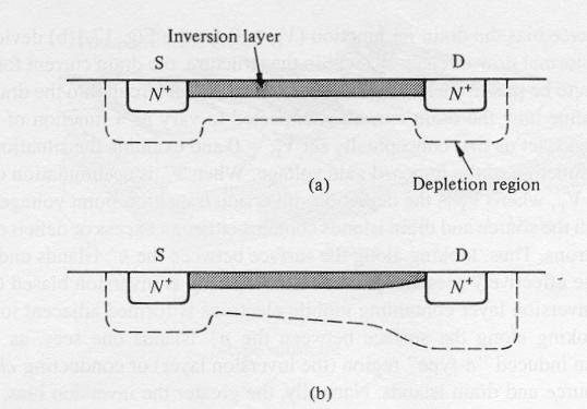
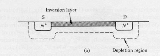
42 Qualitative MOSFET Operation Depletion Layer

43 Channel Length Modulation
 0 n( x,")
44 MOSFET I-V Characteristics A 1 st attempt The Square Law Theory Current in the channel should be mainly drift-driven dφ J N qμnnε qμnn dy The current is: I D qz J Z μ Q dφ μn dy n N Ny dx dz x c dφ dy ( y) 0 n( x, y) dx
45 MOSFET I-V Characteristics A 1 st attempt But, current is constant through the channel: We know the inversion layer charge: Accounting for the non-uniformity: D D V N n D V N n D L D d Q L Z I d Q Z L I dy I φ μ φ μ ) ( T G ox inv V V C Q ) ( ) ( φ T G ox inv V V C y Q ( ) T G Dsat D D D T G ox n D V V V V V V V V C L Z I K μ
46 MOSFET I-V Characteristics A 1 st attempt Past pinch-off, the drain current is constant I D, V D So: > V I D, V V Dsat Dsat Dsat Now, in the pinched-off region: I D Q V I D inv Dsat ( y) V Z L G D μ C n ox V Z μnc 2L T ox G C ( V V V ) 0 ox I 2 V ( V ) Dsat G VT VDsat T [ V V ] 2 G T Dsat 2
47 N-channel MOSFET Layout (Top View) 4 lithography steps are required: 1. active area 2. gate electrode 3. contacts 4. metal interconnects
48 Simple NMOS Process Flow 1) Thermal oxidation (~10 nm pad oxide ) 2) Silicon-nitride (Si 3 N 4 ) deposition by CVD (~40nm) 3) Active-area definition (lithography & etch) 4) Boron ion implantation ( channel stop implant)
49 5) Thermal oxidation to grow oxide in field regions 6) Si 3 N 4 & pad oxide removal 7) Thermal oxidation ( gate oxide ) 8) Poly-Si deposition by CVD 9) Poly-Si gate-electrode patterning (litho. & etch) Simple NMOS Process Flow 10) P or As ion implantation to form n+ source and drain regions Top view of masks
50 Simple NMOS Process Flow 11) SiO 2 CVD Top view of masks 12) Contact definition (litho. & etch) 13) Al deposition by sputtering 14) Al patterning by litho. & etch to form interconnects
Section 12: Intro to Devices
 Section 12: Intro to Devices Extensive reading materials on reserve, including Robert F. Pierret, Semiconductor Device Fundamentals EE143 Ali Javey Bond Model of Electrons and Holes Si Si Si Si Si Si Si
Extensive reading materials on reserve, including
 Section 12: Intro to Devices Extensive reading materials on reserve, including Robert F. Pierret, Semiconductor Device Fundamentals EE143 Ali Javey Bond Model of Electrons and Holes Si Si Si Si Si Si Si
Electrical Characteristics of MOS Devices
 Electrical Characteristics of MOS Devices The MOS Capacitor Voltage components Accumulation, Depletion, Inversion Modes Effect of channel bias and substrate bias Effect of gate oide charges Threshold-voltage
MOS CAPACITOR AND MOSFET
 EE336 Semiconductor Devices 1 MOS CAPACITOR AND MOSFET Dr. Mohammed M. Farag Ideal MOS Capacitor Semiconductor Devices Physics and Technology Chapter 5 EE336 Semiconductor Devices 2 MOS Capacitor Structure
Electrical Resistance
 Electrical Resistance I + V _ W Material with resistivity ρ t L Resistance R V I = L ρ Wt (Unit: ohms) where ρ is the electrical resistivity 1 Adding parts/billion to parts/thousand of dopants to pure
Lecture 12: MOS Capacitors, transistors. Context
 Lecture 12: MOS Capacitors, transistors Context In the last lecture, we discussed PN diodes, and the depletion layer into semiconductor surfaces. Small signal models In this lecture, we will apply those
Semiconductor Devices. C. Hu: Modern Semiconductor Devices for Integrated Circuits Chapter 5
 Semiconductor Devices C. Hu: Modern Semiconductor Devices for Integrated Circuits Chapter 5 Global leader in environmental and industrial measurement Wednesday 3.2. afternoon Tour around facilities & lecture
Semiconductor Physics Problems 2015
 Semiconductor Physics Problems 2015 Page and figure numbers refer to Semiconductor Devices Physics and Technology, 3rd edition, by SM Sze and M-K Lee 1. The purest semiconductor crystals it is possible
ESE 570: Digital Integrated Circuits and VLSI Fundamentals
 ESE 570: Digital Integrated Circuits and VLSI Fundamentals Lec 4: January 24, 2017 MOS Transistor Theory, MOS Model Penn ESE 570 Spring 2017 Khanna Lecture Outline! Semiconductor Physics " Band gaps "
ESE 570: Digital Integrated Circuits and VLSI Fundamentals
 ESE 570: Digital Integrated Circuits and VLSI Fundamentals Lec 4: January 23, 2018 MOS Transistor Theory, MOS Model Penn ESE 570 Spring 2018 Khanna Lecture Outline! CMOS Process Enhancements! Semiconductor
Lecture 7 PN Junction and MOS Electrostatics(IV) Metal Oxide Semiconductor Structure (contd.)
 Metal Oxide Semiconductor Structure (contd.)") Lecture 7 PN Junction and MOS Electrostatics(IV) Metal Oxide Semiconductor Structure (contd.) Outline 1. Overview of MOS electrostatics under bias 2. Depletion regime 3. Flatband 4. Accumulation regime
Lecture 7 PN Junction and MOS Electrostatics(IV) Metal Oxide Semiconductor Structure (contd.) Outline 1. Overview of MOS electrostatics under bias 2. Depletion regime 3. Flatband 4. Accumulation regime
The Devices: MOS Transistors
 The Devices: MOS Transistors References: Semiconductor Device Fundamentals, R. F. Pierret, Addison-Wesley Digital Integrated Circuits: A Design Perspective, J. Rabaey et.al. Prentice Hall NMOS Transistor
UNIVERSITY OF CALIFORNIA College of Engineering Department of Electrical Engineering and Computer Sciences. EECS 130 Professor Ali Javey Fall 2006
 UNIVERSITY OF CALIFORNIA College of Engineering Department of Electrical Engineering and Computer Sciences EECS 130 Professor Ali Javey Fall 2006 Midterm 2 Name: SID: Closed book. Two sheets of notes are
ESE 570: Digital Integrated Circuits and VLSI Fundamentals
 ESE 570: Digital Integrated Circuits and VLSI Fundamentals Lec 4: January 29, 2019 MOS Transistor Theory, MOS Model Penn ESE 570 Spring 2019 Khanna Lecture Outline! CMOS Process Enhancements! Semiconductor
MOS Capacitor MOSFET Devices. MOSFET s. INEL Solid State Electronics. Manuel Toledo Quiñones. ECE Dept. UPRM.
 INEL 6055 - Solid State Electronics ECE Dept. UPRM 20th March 2006 Definitions MOS Capacitor Isolated Metal, SiO 2, Si Threshold Voltage qφ m metal d vacuum level SiO qχ 2 E g /2 qφ F E C E i E F E v qφ
Lecture 2. Introduction to semiconductors Structures and characteristics in semiconductors
 Lecture 2 Introduction to semiconductors Structures and characteristics in semiconductors Semiconductor p-n junction Metal Oxide Silicon structure Semiconductor contact Literature Glen F. Knoll, Radiation
Lecture 04 Review of MOSFET
 ECE 541/ME 541 Microelectronic Fabrication Techniques Lecture 04 Review of MOSFET Zheng Yang (ERF 3017, email: yangzhen@uic.edu) What is a Transistor? A Switch! An MOS Transistor V GS V T V GS S Ron D
Quiz #1 Practice Problem Set
 Name: Student Number: ELEC 3908 Physical Electronics Quiz #1 Practice Problem Set? Minutes January 22, 2016 - No aids except a non-programmable calculator - All questions must be answered - All questions
Lecture 11: MOS Transistor
 Lecture 11: MOS Transistor Prof. Niknejad Lecture Outline Review: MOS Capacitors Regions MOS Capacitors (3.8 3.9) CV Curve Threshold Voltage MOS Transistors (4.1 4.3): Overview Cross-section and layout
Lecture 6 PN Junction and MOS Electrostatics(III) Metal-Oxide-Semiconductor Structure
 Metal-Oxide-Semiconductor Structure") Lecture 6 PN Junction and MOS Electrostatics(III) Metal-Oxide-Semiconductor Structure Outline 1. Introduction to MOS structure 2. Electrostatics of MOS in thermal equilibrium 3. Electrostatics of MOS with
Lecture 6 PN Junction and MOS Electrostatics(III) Metal-Oxide-Semiconductor Structure Outline 1. Introduction to MOS structure 2. Electrostatics of MOS in thermal equilibrium 3. Electrostatics of MOS with
! CMOS Process Enhancements. ! Semiconductor Physics. " Band gaps. " Field Effects. ! MOS Physics. " Cut-off. " Depletion.
 ESE 570: Digital Integrated Circuits and VLSI Fundamentals Lec 4: January 9, 019 MOS Transistor Theory, MOS Model Lecture Outline CMOS Process Enhancements Semiconductor Physics Band gaps Field Effects
Classification of Solids
 Classification of Solids Classification by conductivity, which is related to the band structure: (Filled bands are shown dark; D(E) = Density of states) Class Electron Density Density of States D(E) Examples
Lecture 15 OUTLINE. MOSFET structure & operation (qualitative) Review of electrostatics The (N)MOS capacitor
 Review of electrostatics The (N)MOS capacitor") Lecture 15 OUTLINE MOSFET structure & operation (qualitative) Review of electrostatics The (N)MOS capacitor Electrostatics Charge vs. voltage characteristic Reading: Chapter 6.1 6.2.1 EE15 Spring 28 Lecture
Lecture 15 OUTLINE MOSFET structure & operation (qualitative) Review of electrostatics The (N)MOS capacitor Electrostatics Charge vs. voltage characteristic Reading: Chapter 6.1 6.2.1 EE15 Spring 28 Lecture
Lecture Outline. ESE 570: Digital Integrated Circuits and VLSI Fundamentals. Review: MOSFET N-Type, P-Type. Semiconductor Physics.
 ESE 57: Digital Integrated Circuits and VLSI Fundamentals Lec 4: January 24, 217 MOS Transistor Theory, MOS Model Lecture Outline! Semiconductor Physics " Band gaps " Field Effects! MOS Physics " Cutoff
MOS Transistor I-V Characteristics and Parasitics
 ECEN454 Digital Integrated Circuit Design MOS Transistor I-V Characteristics and Parasitics ECEN 454 Facts about Transistors So far, we have treated transistors as ideal switches An ON transistor passes
Semiconductor Physics fall 2012 problems
 Semiconductor Physics fall 2012 problems 1. An n-type sample of silicon has a uniform density N D = 10 16 atoms cm -3 of arsenic, and a p-type silicon sample has N A = 10 15 atoms cm -3 of boron. For each
UNIVERSITY OF CALIFORNIA College of Engineering Department of Electrical Engineering and Computer Sciences. Professor Chenming Hu.
 UNIVERSITY OF CALIFORNIA College of Engineering Department of Electrical Engineering and Computer Sciences EECS 130 Spring 2009 Professor Chenming Hu Midterm I Name: Closed book. One sheet of notes is
FIELD-EFFECT TRANSISTORS
 FIEL-EFFECT TRANSISTORS 1 Semiconductor review 2 The MOS capacitor 2 The enhancement-type N-MOS transistor 3 I-V characteristics of enhancement MOSFETS 4 The output characteristic of the MOSFET in saturation
The Devices. Digital Integrated Circuits A Design Perspective. Jan M. Rabaey Anantha Chandrakasan Borivoje Nikolic. July 30, 2002
 igital Integrated Circuits A esign Perspective Jan M. Rabaey Anantha Chandrakasan Borivoje Nikolic The evices July 30, 2002 Goal of this chapter Present intuitive understanding of device operation Introduction
For the following statements, mark ( ) for true statement and (X) for wrong statement and correct it.
 for true statement and (X) for wrong statement and correct it.") Benha University Faculty of Engineering Shoubra Electrical Engineering Department First Year communications. Answer all the following questions Illustrate your answers with sketches when necessary. The
Benha University Faculty of Engineering Shoubra Electrical Engineering Department First Year communications. Answer all the following questions Illustrate your answers with sketches when necessary. The
EECS130 Integrated Circuit Devices
 EECS130 Integrated Circuit Devices Professor Ali Javey 9/18/2007 P Junctions Lecture 1 Reading: Chapter 5 Announcements For THIS WEEK OLY, Prof. Javey's office hours will be held on Tuesday, Sept 18 3:30-4:30
Lecture 15 OUTLINE. MOSFET structure & operation (qualitative) Review of electrostatics The (N)MOS capacitor
 Review of electrostatics The (N)MOS capacitor") Lecture 15 OUTLINE MOSFET structure & operation (qualitative) Review of electrostatics The (N)MOS capacitor Electrostatics t ti Charge vs. voltage characteristic Reading: Chapter 6.1 6.2.1 EE105 Fall 2007
Lecture 15 OUTLINE MOSFET structure & operation (qualitative) Review of electrostatics The (N)MOS capacitor Electrostatics t ti Charge vs. voltage characteristic Reading: Chapter 6.1 6.2.1 EE105 Fall 2007
an introduction to Semiconductor Devices
 an introduction to Semiconductor Devices Donald A. Neamen Chapter 6 Fundamentals of the Metal-Oxide-Semiconductor Field-Effect Transistor Introduction: Chapter 6 1. MOSFET Structure 2. MOS Capacitor -
Appendix 1: List of symbols
 Appendix 1: List of symbols Symbol Description MKS Units a Acceleration m/s 2 a 0 Bohr radius m A Area m 2 A* Richardson constant m/s A C Collector area m 2 A E Emitter area m 2 b Bimolecular recombination
! CMOS Process Enhancements. ! Semiconductor Physics. " Band gaps. " Field Effects. ! MOS Physics. " Cut-off. " Depletion.
 ESE 570: Digital Integrated Circuits and VLSI Fundamentals Lec 4: January 3, 018 MOS Transistor Theory, MOS Model Lecture Outline! CMOS Process Enhancements! Semiconductor Physics " Band gaps " Field Effects!
Lecture 2. Introduction to semiconductors Structures and characteristics in semiconductors
 Lecture 2 Introduction to semiconductors Structures and characteristics in semiconductors Semiconductor p-n junction Metal Oxide Silicon structure Semiconductor contact Literature Glen F. Knoll, Radiation
Session 6: Solid State Physics. Diode
 Session 6: Solid State Physics Diode 1 Outline A B C D E F G H I J 2 Definitions / Assumptions Homojunction: the junction is between two regions of the same material Heterojunction: the junction is between
Semiconductor Device Physics
 1 Semiconductor Device Physics Lecture 3 http://zitompul.wordpress.com 2 0 1 3 Semiconductor Device Physics 2 Three primary types of carrier action occur inside a semiconductor: Drift: charged particle
Midterm I - Solutions
 UNIVERSITY OF CALIFORNIA College of Engineering Department of Electrical Engineering and Computer Sciences EECS 130 Spring 2008 Professor Chenming Hu Midterm I - Solutions Name: SID: Grad/Undergrad: Closed
Semiconductor Junctions
 8 Semiconductor Junctions Almost all solar cells contain junctions between different materials of different doping. Since these junctions are crucial to the operation of the solar cell, we will discuss
Class 05: Device Physics II
 Topics: 1. Introduction 2. NFET Model and Cross Section with Parasitics 3. NFET as a Capacitor 4. Capacitance vs. Voltage Curves 5. NFET as a Capacitor - Band Diagrams at V=0 6. NFET as a Capacitor - Accumulation
Final Examination EE 130 December 16, 1997 Time allotted: 180 minutes
 Final Examination EE 130 December 16, 1997 Time allotted: 180 minutes Problem 1: Semiconductor Fundamentals [30 points] A uniformly doped silicon sample of length 100µm and cross-sectional area 100µm 2
n N D n p = n i p N A
 Summary of electron and hole concentration in semiconductors Intrinsic semiconductor: E G n kt i = pi = N e 2 0 Donor-doped semiconductor: n N D where N D is the concentration of donor impurity Acceptor-doped
ECE 340 Lecture 39 : MOS Capacitor II
 ECE 340 Lecture 39 : MOS Capacitor II Class Outline: Effects of Real Surfaces Threshold Voltage MOS Capacitance-Voltage Analysis Things you should know when you leave Key Questions What are the effects
EECS130 Integrated Circuit Devices
 EECS130 Integrated Circuit Devices Professor Ali Javey 8/30/2007 Semiconductor Fundamentals Lecture 2 Read: Chapters 1 and 2 Last Lecture: Energy Band Diagram Conduction band E c E g Band gap E v Valence
Student Number: CARLETON UNIVERSITY SELECTED FINAL EXAMINATION QUESTIONS
 Name: CARLETON UNIVERSITY SELECTE FINAL EXAMINATION QUESTIONS URATION: 6 HOURS epartment Name & Course Number: ELEC 3908 Course Instructors: S. P. McGarry Authorized Memoranda: Non-programmable calculators
MOS Transistors. Prof. Krishna Saraswat. Department of Electrical Engineering Stanford University Stanford, CA
 MOS Transistors Prof. Krishna Saraswat Department of Electrical Engineering S Stanford, CA 94305 saraswat@stanford.edu 1 1930: Patent on the Field-Effect Transistor! Julius Lilienfeld filed a patent describing
Chapter 1 Overview of Semiconductor Materials and Physics
 Chapter 1 Overview of Semiconductor Materials and Physics Professor Paul K. Chu Conductivity / Resistivity of Insulators, Semiconductors, and Conductors Semiconductor Elements Period II III IV V VI 2 B
Choice of V t and Gate Doping Type
 Choice of V t and Gate Doping Type To make circuit design easier, it is routine to set V t at a small positive value, e.g., 0.4 V, so that, at V g = 0, the transistor does not have an inversion layer and
CMPEN 411 VLSI Digital Circuits. Lecture 03: MOS Transistor
 CMPEN 411 VLSI Digital Circuits Lecture 03: MOS Transistor Kyusun Choi [Adapted from Rabaey s Digital Integrated Circuits, Second Edition, 2003 J. Rabaey, A. Chandrakasan, B. Nikolic] CMPEN 411 L03 S.1
Semiconductor Physics fall 2012 problems
 Semiconductor Physics fall 2012 problems 1. An n-type sample of silicon has a uniform density N D = 10 16 atoms cm -3 of arsenic, and a p-type silicon sample has N A = 10 15 atoms cm -3 of boron. For each
MOSFET: Introduction
 E&CE 437 Integrated VLSI Systems MOS Transistor 1 of 30 MOSFET: Introduction Metal oxide semiconductor field effect transistor (MOSFET) or MOS is widely used for implementing digital designs Its major
EECS130 Integrated Circuit Devices
 EECS130 Integrated Circuit Devices Professor Ali Javey 10/02/2007 MS Junctions, Lecture 2 MOS Cap, Lecture 1 Reading: finish chapter14, start chapter16 Announcements Professor Javey will hold his OH at
Review Energy Bands Carrier Density & Mobility Carrier Transport Generation and Recombination
 Review Energy Bands Carrier Density & Mobility Carrier Transport Generation and Recombination The Metal-Semiconductor Junction: Review Energy band diagram of the metal and the semiconductor before (a)
Lecture 15 - The pn Junction Diode (I) I-V Characteristics. November 1, 2005
 I-V Characteristics. November 1, 2005") 6.012 - Microelectronic Devices and Circuits - Fall 2005 Lecture 15-1 Lecture 15 - The pn Junction Diode (I) I-V Characteristics November 1, 2005 Contents: 1. pn junction under bias 2. I-V characteristics
6.012 - Microelectronic Devices and Circuits - Fall 2005 Lecture 15-1 Lecture 15 - The pn Junction Diode (I) I-V Characteristics November 1, 2005 Contents: 1. pn junction under bias 2. I-V characteristics
PN Junction and MOS structure
 PN Junction and MOS structure Basic electrostatic equations We will use simple one-dimensional electrostatic equations to develop insight and basic understanding of how semiconductor devices operate Gauss's
1 Name: Student number: DEPARTMENT OF PHYSICS AND PHYSICAL OCEANOGRAPHY MEMORIAL UNIVERSITY OF NEWFOUNDLAND. Fall :00-11:00
 1 Name: DEPARTMENT OF PHYSICS AND PHYSICAL OCEANOGRAPHY MEMORIAL UNIVERSITY OF NEWFOUNDLAND Final Exam Physics 3000 December 11, 2012 Fall 2012 9:00-11:00 INSTRUCTIONS: 1. Answer all seven (7) questions.
Integrated Circuits & Systems
 Federal University of Santa Catarina Center for Technology Computer Science & Electronics Engineering Integrated Circuits & Systems INE 5442 Lecture 10 MOSFET part 1 guntzel@inf.ufsc.br ual-well Trench-Isolated
Chapter 7. The pn Junction
 Chapter 7 The pn Junction Chapter 7 PN Junction PN junction can be fabricated by implanting or diffusing donors into a P-type substrate such that a layer of semiconductor is converted into N type. Converting
Digital Integrated Circuits A Design Perspective. Jan M. Rabaey Anantha Chandrakasan Borivoje Nikolic. The Devices. July 30, Devices.
 Digital Integrated Circuits A Design Perspective Jan M. Rabaey Anantha Chandrakasan Borivoje Nikolic The July 30, 2002 1 Goal of this chapter Present intuitive understanding of device operation Introduction
Charge Carriers in Semiconductor
 Charge Carriers in Semiconductor To understand PN junction s IV characteristics, it is important to understand charge carriers behavior in solids, how to modify carrier densities, and different mechanisms
Fundamentals of the Metal Oxide Semiconductor Field-Effect Transistor
 Triode Working FET Fundamentals of the Metal Oxide Semiconductor Field-Effect Transistor The characteristics of energy bands as a function of applied voltage. Surface inversion. The expression for the
Diodes. anode. cathode. cut-off. Can be approximated by a piecewise-linear-like characteristic. Lecture 9-1
 Diodes mplest nonlinear circuit element Basic operation sets the foundation for Bipolar Junction Transistors (BJTs) Also present in Field Effect Transistors (FETs) Ideal diode characteristic anode cathode
EE105 - Fall 2006 Microelectronic Devices and Circuits
 EE105 - Fall 2006 Microelectronic Devices and Circuits Prof. Jan M. Rabaey (jan@eecs) Lecture 7: MOS Transistor Some Administrative Issues Lab 2 this week Hw 2 due on We Hw 3 will be posted same day MIDTERM
The Devices. Digital Integrated Circuits A Design Perspective. Jan M. Rabaey Anantha Chandrakasan Borivoje Nikolic. July 30, 2002
 Digital Integrated Circuits A Design Perspective Jan M. Rabaey Anantha Chandrakasan Borivoje Nikolic The Devices July 30, 2002 Goal of this chapter Present intuitive understanding of device operation Introduction
SECTION: Circle one: Alam Lundstrom. ECE 305 Exam 5 SOLUTIONS: Spring 2016 April 18, 2016 M. A. Alam and M.S. Lundstrom Purdue University
 NAME: PUID: SECTION: Circle one: Alam Lundstrom ECE 305 Exam 5 SOLUTIONS: April 18, 2016 M A Alam and MS Lundstrom Purdue University This is a closed book exam You may use a calculator and the formula
1. The MOS Transistor. Electrical Conduction in Solids
 Electrical Conduction in Solids!The band diagram describes the energy levels for electron in solids.!the lower filled band is named Valence Band.!The upper vacant band is named conduction band.!the distance
EE 560 MOS TRANSISTOR THEORY
 1 EE 560 MOS TRANSISTOR THEORY PART 1 TWO TERMINAL MOS STRUCTURE V G (GATE VOLTAGE) 2 GATE OXIDE SiO 2 SUBSTRATE p-type doped Si (N A = 10 15 to 10 16 cm -3 ) t ox V B (SUBSTRATE VOLTAGE) EQUILIBRIUM:
Lecture 3 Semiconductor Physics (II) Carrier Transport
 Carrier Transport") Lecture 3 Semiconductor Physics (II) Carrier Transport Thermal Motion Carrier Drift Carrier Diffusion Outline Reading Assignment: Howe and Sodini; Chapter 2, Sect. 2.4-2.6 6.012 Spring 2009 Lecture 3 1
Lecture 3 Semiconductor Physics (II) Carrier Transport Thermal Motion Carrier Drift Carrier Diffusion Outline Reading Assignment: Howe and Sodini; Chapter 2, Sect. 2.4-2.6 6.012 Spring 2009 Lecture 3 1
Long-channel MOSFET IV Corrections
 Long-channel MOSFET IV orrections Three MITs of the Day The body ect and its influence on long-channel V th. Long-channel subthreshold conduction and control (subthreshold slope S) Scattering components
Lecture 2. Introduction to semiconductors Structures and characteristics in semiconductors. Fabrication of semiconductor sensor
 Lecture 2 Introduction to semiconductors Structures and characteristics in semiconductors Semiconductor p-n junction Metal Oxide Silicon structure Semiconductor contact Fabrication of semiconductor sensor
collisions of electrons. In semiconductor, in certain temperature ranges the conductivity increases rapidly by increasing temperature
 1.9. Temperature Dependence of Semiconductor Conductivity Such dependence is one most important in semiconductor. In metals, Conductivity decreases by increasing temperature due to greater frequency of
Lecture #27. The Short Channel Effect (SCE)
") Lecture #27 ANNOUNCEMENTS Design Project: Your BJT design should meet the performance specifications to within 10% at both 300K and 360K. ( β dc > 45, f T > 18 GHz, V A > 9 V and V punchthrough > 9 V )
Lecture #27 ANNOUNCEMENTS Design Project: Your BJT design should meet the performance specifications to within 10% at both 300K and 360K. ( β dc > 45, f T > 18 GHz, V A > 9 V and V punchthrough > 9 V )
ESE 570 MOS TRANSISTOR THEORY Part 1. Kenneth R. Laker, University of Pennsylvania, updated 5Feb15
 ESE 570 MOS TRANSISTOR THEORY Part 1 TwoTerminal MOS Structure 2 GATE Si Oxide interface n n Mass Action Law VB 2 Chemical Periodic Table Donors American Chemical Society (ACS) Acceptors Metalloids 3 Ideal
Chapter 2. Electronics I - Semiconductors
 Chapter 2 Electronics I - Semiconductors Fall 2017 talarico@gonzaga.edu 1 Charged Particles The operation of all electronic devices is based on controlling the flow of charged particles There are two type
Sample Exam # 2 ECEN 3320 Fall 2013 Semiconductor Devices October 28, 2013 Due November 4, 2013
 Sample Exam # 2 ECEN 3320 Fall 203 Semiconductor Devices October 28, 203 Due November 4, 203. Below is the capacitance-voltage curve measured from a Schottky contact made on GaAs at T 300 K. Figure : Capacitance
Lecture 3: CMOS Transistor Theory
 Lecture 3: CMOS Transistor Theory Outline Introduction MOS Capacitor nmos I-V Characteristics pmos I-V Characteristics Gate and Diffusion Capacitance 2 Introduction So far, we have treated transistors
UNIVERSITY OF CALIFORNIA College of Engineering Department of Electrical Engineering and Computer Sciences. EECS 130 Professor Ali Javey Fall 2006
 UNIVERSITY OF CALIFORNIA College of Engineering Department of Electrical Engineering and Computer Sciences EECS 130 Professor Ali Javey Fall 2006 Midterm I Name: Closed book. One sheet of notes is allowed.
ECE 142: Electronic Circuits Lecture 3: Semiconductors
 Faculty of Engineering ECE 142: Electronic Circuits Lecture 3: Semiconductors Agenda Intrinsic Semiconductors Extrinsic Semiconductors N-type P-type Carrier Transport Drift Diffusion Semiconductors A semiconductor
Week 3, Lectures 6-8, Jan 29 Feb 2, 2001
 Week 3, Lectures 6-8, Jan 29 Feb 2, 2001 EECS 105 Microelectronics Devices and Circuits, Spring 2001 Andrew R. Neureuther Topics: M: Charge density, electric field, and potential; W: Capacitance of pn
Semiconductor Detectors are Ionization Chambers. Detection volume with electric field Energy deposited positive and negative charge pairs
 1 V. Semiconductor Detectors V.1. Principles Semiconductor Detectors are Ionization Chambers Detection volume with electric field Energy deposited positive and negative charge pairs Charges move in field
ESE 372 / Spring 2013 / Lecture 5 Metal Oxide Semiconductor Field Effect Transistor
 Metal Oxide Semiconductor Field Effect Transistor V G V G 1 Metal Oxide Semiconductor Field Effect Transistor We will need to understand how this current flows through Si What is electric current? 2 Back
Semiconductor Integrated Process Design (MS 635)
") Semiconductor Integrated Process Design (MS 635) Instructor: Prof. Keon Jae Lee - Office: 응용공학동 #4306, Tel: #3343 - Email: keonlee@kaist.ac.kr Lecture: (Tu, Th), 1:00-2:15 #2425 Office hour: Tues & Thur
Semiconductor Integrated Process Design (MS 635) Instructor: Prof. Keon Jae Lee - Office: 응용공학동 #4306, Tel: #3343 - Email: keonlee@kaist.ac.kr Lecture: (Tu, Th), 1:00-2:15 #2425 Office hour: Tues & Thur
Theory of Electrical Characterization of Semiconductors
 Theory of Electrical Characterization of Semiconductors P. Stallinga Universidade do Algarve U.C.E.H. A.D.E.E.C. OptoElectronics SELOA Summer School May 2000, Bologna (It) Overview Devices: bulk Schottky
Semiconductor Detectors
 Semiconductor Detectors Summary of Last Lecture Band structure in Solids: Conduction band Conduction band thermal conductivity: E g > 5 ev Valence band Insulator Charge carrier in conductor: e - Charge
Lecture 8 PN Junction and MOS Electrostatics (V) Electrostatics of Metal Oxide Semiconductor Structure (cont.) October 4, 2005
 Electrostatics of Metal Oxide Semiconductor Structure (cont.) October 4, 2005") 6.12 Microelectronic Devices and Circuits Fall 25 Lecture 8 1 Lecture 8 PN Junction and MOS Electrostatics (V) Electrostatics of Metal Oide Semiconductor Structure (cont.) Contents: October 4, 25 1. Overview
6.12 Microelectronic Devices and Circuits Fall 25 Lecture 8 1 Lecture 8 PN Junction and MOS Electrostatics (V) Electrostatics of Metal Oide Semiconductor Structure (cont.) Contents: October 4, 25 1. Overview
Current mechanisms Exam January 27, 2012
 Current mechanisms Exam January 27, 2012 There are four mechanisms that typically cause currents to flow: thermionic emission, diffusion, drift, and tunneling. Explain briefly which kind of current mechanisms
Session 0: Review of Solid State Devices. From Atom to Transistor
 Session 0: Review of Solid State Devices From Atom to Transistor 1 Objective To Understand: how Diodes, and Transistors operate! p n p+ n p- n+ n+ p 2 21 Century Alchemy! Ohm s law resistivity Resistivity
EECS143 Microfabrication Technology
 EECS143 Microfabrication Technology Professor Ali Javey Introduction to Materials Lecture 1 Evolution of Devices Yesterday s Transistor (1947) Today s Transistor (2006) Why Semiconductors? Conductors e.g
Lecture 12: MOSFET Devices
 Lecture 12: MOSFET Devices Gu-Yeon Wei Division of Engineering and Applied Sciences Harvard University guyeon@eecs.harvard.edu Wei 1 Overview Reading S&S: Chapter 5.1~5.4 Supplemental Reading Background
Content. MIS Capacitor. Accumulation Depletion Inversion MOS CAPACITOR. A Cantoni Digital Switching
 Content MIS Capacitor Accumulation Depletion Inversion MOS CAPACITOR 1 MIS Capacitor Metal Oxide C ox p-si C s Components of a capacitance model for the MIS structure 2 MIS Capacitor- Accumulation ρ( x)
ESE370: Circuit-Level Modeling, Design, and Optimization for Digital Systems
 ESE370: Circuit-Level Modeling, Design, and Optimization for Digital Systems Lec 6: September 14, 2015 MOS Model You are Here: Transistor Edition! Previously: simple models (0 and 1 st order) " Comfortable
Carrier transport: Drift and Diffusion
 . Carrier transport: Drift and INEL 5209 - Solid State Devices - Spring 2012 Manuel Toledo April 10, 2012 Manuel Toledo Transport 1/ 32 Outline...1 Drift Drift current Mobility Resistivity Resistance Hall
PHYS208 P-N Junction. Olav Torheim. May 30, 2007
 1 PHYS208 P-N Junction Olav Torheim May 30, 2007 1 Intrinsic semiconductors The lower end of the conduction band is a parabola, just like in the quadratic free electron case (E = h2 k 2 2m ). The density
ECE 305 Exam 5 SOLUTIONS: Spring 2015 April 17, 2015 Mark Lundstrom Purdue University
 NAME: PUID: : ECE 305 Exam 5 SOLUTIONS: April 17, 2015 Mark Lundstrom Purdue University This is a closed book exam. You may use a calculator and the formula sheet at the end of this exam. Following the
Device Models (PN Diode, MOSFET )
") Device Models (PN Diode, MOSFET ) Instructor: Steven P. Levitan steve@ece.pitt.edu TA: Gayatri Mehta, José Martínez Book: Digital Integrated Circuits: A Design Perspective; Jan Rabaey Lab Notes: Handed
Device Models (PN Diode, MOSFET ) Instructor: Steven P. Levitan steve@ece.pitt.edu TA: Gayatri Mehta, José Martínez Book: Digital Integrated Circuits: A Design Perspective; Jan Rabaey Lab Notes: Handed
PN Junction
 P Junction 2017-05-04 Definition Power Electronics = semiconductor switches are used Analogue amplifier = high power loss 250 200 u x 150 100 u Udc i 50 0 0 50 100 150 200 250 300 350 400 i,u dc i,u u
Semiconductor Physics and Devices
 The pn Junction 1) Charge carriers crossing the junction. 3) Barrier potential Semiconductor Physics and Devices Chapter 8. The pn Junction Diode 2) Formation of positive and negative ions. 4) Formation
Spring Semester 2012 Final Exam
 Spring Semester 2012 Final Exam Note: Show your work, underline results, and always show units. Official exam time: 2.0 hours; an extension of at least 1.0 hour will be granted to anyone. Materials parameters
Objective: The purpose of these notes is to familiarize students with semiconductors and devices including the P-N junction, and the transistors.
 - 1-1/15/02C:\lec320.doc H.L.Kwok SEMICONDUCTOR MATERIALS AND DEVICES by H.L. Kwok Objective: The purpose of these notes is to familiarize students with semiconductors and devices including the P-N junction,