PHYS208 P-N Junction. Olav Torheim. May 30, 2007
|
|
|
- MargaretMargaret Lawson
- 6 years ago
- Views:
Transcription
1 1 PHYS208 P-N Junction Olav Torheim May 30, 2007
2
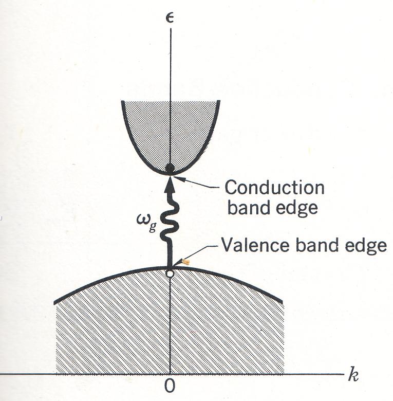
3 1 Intrinsic semiconductors The lower end of the conduction band is a parabola, just like in the quadratic free electron case (E = h2 k 2 2m ). The density of states for free particles in a box is: g(e) = V 3/2 2m 2π 2 h 2 E 1/2 We assume that the electrons in the conduction band behave like free electrons, and therefore use the the same density of states as for the free electron model. We only correct for the effective mass and that we have to count the energy from the bottom of the conduction band and up: g c (E) = V 3/2 2m 2π 2 h 2 (E E c ) 1/2 The number of free electrons in the conduction band is then given by the following integral:
4 N c = g c (E) f F D (E)dE = 2V ( m kt 3/2 E c 2π h 2 ) e µ Ec We can make the same calculation for the number of holes in the valence band if we use the effective mass for holes and integrate from the top of the valence band and down to inifinity. Here we also have to take into consideration that f h (E) = 1 f F D (E). N v = E v g v (E) (1 f F D )(E)dE = 2V ( m 3/2 h kt 2π h 2 ) e Ev µ The chemical potential of the intrinsic semiconductor is found be setting N c = N v : µ = E c + E v kt ln(m h m e ) Which shows that the chemical potential must be in the middle of the energy gap:
5
6 In the same way, we can find the intrinsic carrier concentration by multiplying N c /V and N v /V : n 2 i = n c n v = 4 m e m h 3/4 (kt/2π h 2 ) 3 e Eg/kT The intrinsic carrier concentration is dependent only on the energi gap and not on the Fermi level (which means that the law of mass action, n c n v = n 2 i, is valid also for doped semiconductors). 2 Doped semiconductors Impurity atoms are added to provide loosely bound electrons (n-doping with group 5 material) or holes (p-doping with group 3 material) that are thermally excited to the conduction or valence band. The impurity atoms are usually not close enough for the wavefunctions to overlap, therefore the impurity states are localized. Their energy levels are either right below the conduction band or right above the valence band. How close they are can be approximated with a modified hydrogen atom model:
7 E ion = 13.6eV m m ɛ 0 2 ɛ Here the electron mass m is replaced by the effective mass m and the dielectricity constant refers to the crystal and not to free space. Example: Phoshorus n-doping of silicon. ɛ r = 11.7 and m is 0.19 near the bottom of the conduction band for Si, which gives us E ion = 0.019eV. The donor m impurity therefore requires 0.019eV to become ionized and the position in the band gap of the donor impurity level is just ev below the conduction band edge. It can be shown using similar arguments as in the intrinsic case that the Fermi level in the n-doped case is in the middle between the band egdes and the impurity states: E F = E c + E d 2
8
9 And in the p-doped case: E F = E v + E a 2 Since the electrons in the semiconductors are modeled as Bloch electrons, they all have a nonvanishing group velocity. On the band edges this group velocity is v g = 1 h de = 0. This implies that the kinetic energy on the band egde is dk zero, and the position of the band egde as a function of position is therefore changing in the same way as the potential energy is changing.
10 When p-doped and n-doped materials are joined, there is an inbalance between the n-type and p-type carrier concentrations on each side because of the different Fermi levels. N-type and p-type majority carriers will therefore diffuse into each others regions and recombine until a potential is built up that opposes the diffusion currents. The potential is called the built-in-potential, φ BI, and it raises the band edges on the p-side so the Fermi levels on each side are aligned:
11 After equilibrium is established, there is balance between the diffusion current caused by the carrier inhomogenity (given by Ficks law) and the drift current caused by the electric field (given by simple kinetic free electron theory): which leads to n(x)µe( x x) = D dn dx E x (x) = D µ 1 n dn dx The built-in potential can now be calculated: φ BI = φ( ) φ( ) = E x dx = D µ 1 n(x) dn dx dx = D n( ) ln µ n( ) Now we have the condition for the energy difference, but D, n( ) and n( ) µ are still unknown. It is therefore time to introduce Einstein-Nernst. We start by writing the electric field as the gradient of the potential:
12 E x (x) = dφ dx Therefore µ n e dφ dx = ed dn dx So dn dφ = µ n D The different equation has the solution n = n 0 e µ D φ But because this non-uniform electron distribution has to be maintaned against the potential φ using thermal energy, we must also have
13 n = n 0 e eφ kt φ Thus we finally arrive at the Einstein-Nernst relation: µ D = Now we continue to evaluate ln n( ). In the n-region the density of free n( ) electrons is approximately n( ) = N D. In the p-region, the negative carrier concentration is taken from the law of mass action, n( ) = n2 i N A. From this we obtain the built-in potential: e kt φ BI = D µ lnn( ) = kt e lnn AN D n 2 i After establishing equilibrum between drift and diffusion currents, we are left with a depletion region in the middle of the junction where the holes and
14 electrons have recombined and we have approximately no free carriers. Starting out with the Poisson equation, we can make a model of this depletion region characterized by the parameters kt e, N A and N D : d2 V dx 2 = Cρ(x) The net charge density, ρ, is approximated as zero outside the depletion region. Inside the depletion region, we have approximately ρ = qn A on the p side ( d p x 0) and ρ = qn D on the n-side (0 x d n ). Starting on the p side of the depletion region, integration of the Poisson equation yields Another integration yields ɛ = dv dx = en AC(d p + x) V = en A C( x2 2 + d px + d2 p 2 ) = 1 2 en AC(d p + x) 2
15 for d p x 0, so that V (x = 0) = V 1 = en A C d2 p 2. In the same way we have for the n side that V (x = d p ) V (x = 0) = V 2 = en D C d2 n 2. And we have an equation for the total potential across the junction: V C = φ BI + V R = e C 2 (N Ad 2 p + N D d 2 n). We now define d = d p + d n. And since N D d n = N A d p (charge balance), we finally arrive at an equation that combines the potential across the junction with the geometry and the doping profile of the depletion region: V C = 1 N D N A 2 Ced2. N D + N A
16
17 We say that it is impossible to stop the drift current, since there always will be minority carriers on each side of the junction that are thermally excited and swept across the electric field (which is on the order of V/cm). When it comes to the diffusing majority carriers, there will be a Boltzmann distribution on how many carriers that have energy enough to break through the potential barrier. This recombination current is therefore proportional to the Boltzmann factor e qv C/kT. When no external potential is applied, the generation and recombination currents are in equilibrium: i tot = i rec i gen = i gen i gen = 0 (1) When an external potential, φ ext, is applied, the recombination current is increased with the Boltzmann factor e qφext/kt, while the generation current remains the same: i tot = i gen e qφext/kt i gen = i gen (e qφext/kt 1) (2) which shows us that the p-n junction acts as a rectifier.
18
PHYS208 p-n junction. January 15, 2010
 1 PHYS208 p-n junction January 15, 2010 List of topics (1) Density of states Fermi-Dirac distribution Law of mass action Doped semiconductors Dopinglevel p-n-junctions 1 Intrinsic semiconductors List of
n N D n p = n i p N A
 Summary of electron and hole concentration in semiconductors Intrinsic semiconductor: E G n kt i = pi = N e 2 0 Donor-doped semiconductor: n N D where N D is the concentration of donor impurity Acceptor-doped
ECE 340 Lecture 21 : P-N Junction II Class Outline:
 ECE 340 Lecture 21 : P-N Junction II Class Outline: Contact Potential Equilibrium Fermi Levels Things you should know when you leave Key Questions What is the contact potential? Where does the transition
Charge Carriers in Semiconductor
 Charge Carriers in Semiconductor To understand PN junction s IV characteristics, it is important to understand charge carriers behavior in solids, how to modify carrier densities, and different mechanisms
ESE 372 / Spring 2013 / Lecture 5 Metal Oxide Semiconductor Field Effect Transistor
 Metal Oxide Semiconductor Field Effect Transistor V G V G 1 Metal Oxide Semiconductor Field Effect Transistor We will need to understand how this current flows through Si What is electric current? 2 Back
Semiconductor Junctions
 8 Semiconductor Junctions Almost all solar cells contain junctions between different materials of different doping. Since these junctions are crucial to the operation of the solar cell, we will discuss
ECE 440 Lecture 20 : PN Junction Electrostatics II Class Outline:
 ECE 440 Lecture 20 : PN Junction Electrostatics II Class Outline: Depletion Approximation Step Junction Things you should know when you leave Key Questions What is the space charge region? What are the
ECE 440 Lecture 28 : P-N Junction II Class Outline:
 ECE 440 Lecture 28 : P-N Junction II Class Outline: Contact Potential Equilibrium Fermi Levels Things you should know when you leave Key Questions What is the contact potential? Where does the transition
Chapter 7. The pn Junction
 Chapter 7 The pn Junction Chapter 7 PN Junction PN junction can be fabricated by implanting or diffusing donors into a P-type substrate such that a layer of semiconductor is converted into N type. Converting
Note that it is traditional to draw the diagram for semiconductors rotated 90 degrees, i.e. the version on the right above.
 5 Semiconductors The nearly free electron model applies equally in the case where the Fermi level lies within a small band gap (semiconductors), as it does when the Fermi level lies within a band (metal)
Carriers Concentration and Current in Semiconductors
 Carriers Concentration and Current in Semiconductors Carrier Transport Two driving forces for carrier transport: electric field and spatial variation of the carrier concentration. Both driving forces lead
V BI. H. Föll: kiel.de/matwis/amat/semi_en/kap_2/backbone/r2_2_4.html. different electrochemical potentials (i.e.
 Consider the the band diagram for a homojunction, formed when two bits of the same type of semicondutor (e.g. Si) are doped p and ntype and then brought into contact. Electrons in the two bits have different
Section 12: Intro to Devices
 Section 12: Intro to Devices Extensive reading materials on reserve, including Robert F. Pierret, Semiconductor Device Fundamentals Bond Model of Electrons and Holes Si Si Si Si Si Si Si Si Si Silicon
For the following statements, mark ( ) for true statement and (X) for wrong statement and correct it.
 for true statement and (X) for wrong statement and correct it.") Benha University Faculty of Engineering Shoubra Electrical Engineering Department First Year communications. Answer all the following questions Illustrate your answers with sketches when necessary. The
Benha University Faculty of Engineering Shoubra Electrical Engineering Department First Year communications. Answer all the following questions Illustrate your answers with sketches when necessary. The
Semiconductor Device Physics
 1 Semiconductor Device Physics Lecture 3 http://zitompul.wordpress.com 2 0 1 3 Semiconductor Device Physics 2 Three primary types of carrier action occur inside a semiconductor: Drift: charged particle
Semiconductor Physics and Devices
 The pn Junction 1) Charge carriers crossing the junction. 3) Barrier potential Semiconductor Physics and Devices Chapter 8. The pn Junction Diode 2) Formation of positive and negative ions. 4) Formation
Ch. 2: Energy Bands And Charge Carriers In Semiconductors
 Ch. 2: Energy Bands And Charge Carriers In Semiconductors Discrete energy levels arise from balance of attraction force between electrons and nucleus and repulsion force between electrons each electron
Diodes. anode. cathode. cut-off. Can be approximated by a piecewise-linear-like characteristic. Lecture 9-1
 Diodes mplest nonlinear circuit element Basic operation sets the foundation for Bipolar Junction Transistors (BJTs) Also present in Field Effect Transistors (FETs) Ideal diode characteristic anode cathode
CLASS 12th. Semiconductors
 CLASS 12th Semiconductors 01. Distinction Between Metals, Insulators and Semi-Conductors Metals are good conductors of electricity, insulators do not conduct electricity, while the semiconductors have
Semiconductor Detectors
 Semiconductor Detectors Summary of Last Lecture Band structure in Solids: Conduction band Conduction band thermal conductivity: E g > 5 ev Valence band Insulator Charge carrier in conductor: e - Charge
Solid State Physics SEMICONDUCTORS - IV. Lecture 25. A.H. Harker. Physics and Astronomy UCL
 Solid State Physics SEMICONDUCTORS - IV Lecture 25 A.H. Harker Physics and Astronomy UCL 9.9 Carrier diffusion and recombination Suppose we have a p-type semiconductor, i.e. n h >> n e. (1) Create a local
Lecture 2. Introduction to semiconductors Structures and characteristics in semiconductors
 Lecture 2 Introduction to semiconductors Structures and characteristics in semiconductors Semiconductor p-n junction Metal Oxide Silicon structure Semiconductor contact Literature Glen F. Knoll, Radiation
Consider a uniformly doped PN junction, in which one region of the semiconductor is uniformly doped with acceptor atoms and the adjacent region is
 CHAPTER 7 The PN Junction Consider a uniformly doped PN junction, in which one region of the semiconductor is uniformly doped with acceptor atoms and the adjacent region is uniformly doped with donor atoms.
Effective masses in semiconductors
 Effective masses in semiconductors The effective mass is defined as: In a solid, the electron (hole) effective mass represents how electrons move in an applied field. The effective mass reflects the inverse
ECE 142: Electronic Circuits Lecture 3: Semiconductors
 Faculty of Engineering ECE 142: Electronic Circuits Lecture 3: Semiconductors Agenda Intrinsic Semiconductors Extrinsic Semiconductors N-type P-type Carrier Transport Drift Diffusion Semiconductors A semiconductor
Lecture 15 - The pn Junction Diode (I) I-V Characteristics. November 1, 2005
 I-V Characteristics. November 1, 2005") 6.012 - Microelectronic Devices and Circuits - Fall 2005 Lecture 15-1 Lecture 15 - The pn Junction Diode (I) I-V Characteristics November 1, 2005 Contents: 1. pn junction under bias 2. I-V characteristics
6.012 - Microelectronic Devices and Circuits - Fall 2005 Lecture 15-1 Lecture 15 - The pn Junction Diode (I) I-V Characteristics November 1, 2005 Contents: 1. pn junction under bias 2. I-V characteristics
Carriers Concentration, Current & Hall Effect in Semiconductors. Prof.P. Ravindran, Department of Physics, Central University of Tamil Nadu, India
 Carriers Concentration, Current & Hall Effect in Semiconductors 1 Prof.P. Ravindran, Department of Physics, Central University of Tamil Nadu, India http://folk.uio.no/ravi/semi2013 Conductivity Charge
Isolated atoms Hydrogen Energy Levels. Neuromorphic Engineering I. Solids Energy bands. Metals, semiconductors and insulators Energy bands
 Isolated atoms Hydrogen Energy Levels Neuromorphic Engineering I INI-404 227-1033-00 Electron in atoms have quantized energy levels Material courtesy of Elisabetta Chicca Bielefeld University, Germany
PN Junction
 P Junction 2017-05-04 Definition Power Electronics = semiconductor switches are used Analogue amplifier = high power loss 250 200 u x 150 100 u Udc i 50 0 0 50 100 150 200 250 300 350 400 i,u dc i,u u
Course overview. Me: Dr Luke Wilson. The course: Physics and applications of semiconductors. Office: E17 open door policy
 Course overview Me: Dr Luke Wilson Office: E17 open door policy email: luke.wilson@sheffield.ac.uk The course: Physics and applications of semiconductors 10 lectures aim is to allow time for at least one
PHYS485 Materials Physics
 5/11/017 PHYS485 Materials Physics Dr. Gregory W. Clar Manchester University LET S GO ON A (TEK)ADVENTURE! WHAT? TRIP TO A MAKER S SPACE IN FORT WAYNE WHEN? THURSDAY, MAY 11 TH @ 5PM WHERE? TEKVENTURE
Metal Semiconductor Contacts
 Metal Semiconductor Contacts The investigation of rectification in metal-semiconductor contacts was first described by Braun [33-35], who discovered in 1874 the asymmetric nature of electrical conduction
Semiconductor Physics fall 2012 problems
 Semiconductor Physics fall 2012 problems 1. An n-type sample of silicon has a uniform density N D = 10 16 atoms cm -3 of arsenic, and a p-type silicon sample has N A = 10 15 atoms cm -3 of boron. For each
Lecture 7 - Carrier Drift and Diffusion (cont.) February 20, Non-uniformly doped semiconductor in thermal equilibrium
 February 20, Non-uniformly doped semiconductor in thermal equilibrium") 6.720J/3.43J - Integrated Microelectronic Devices - Spring 2007 Lecture 7-1 Lecture 7 - Carrier Drift and Diffusion (cont.) February 20, 2007 Contents: 1. Non-uniformly doped semiconductor in thermal equilibrium
6.720J/3.43J - Integrated Microelectronic Devices - Spring 2007 Lecture 7-1 Lecture 7 - Carrier Drift and Diffusion (cont.) February 20, 2007 Contents: 1. Non-uniformly doped semiconductor in thermal equilibrium
Due to the quantum nature of electrons, one energy state can be occupied only by one electron.
 In crystalline solids, not all values of the electron energy are possible. The allowed intervals of energy are called allowed bands (shown as blue and chess-board blue). The forbidden intervals are called
Lecture 4 - PN Junction and MOS Electrostatics (I) Semiconductor Electrostatics in Thermal Equilibrium September 20, 2005
 Semiconductor Electrostatics in Thermal Equilibrium September 20, 2005") 6.012 - Microelectronic Devices and Circuits - Fall 2005 Lecture 4-1 Contents: Lecture 4 - PN Junction and MOS Electrostatics (I) Semiconductor Electrostatics in Thermal Equilibrium September 20, 2005
6.012 - Microelectronic Devices and Circuits - Fall 2005 Lecture 4-1 Contents: Lecture 4 - PN Junction and MOS Electrostatics (I) Semiconductor Electrostatics in Thermal Equilibrium September 20, 2005
EECS130 Integrated Circuit Devices
 EECS130 Integrated Circuit Devices Professor Ali Javey 8/30/2007 Semiconductor Fundamentals Lecture 2 Read: Chapters 1 and 2 Last Lecture: Energy Band Diagram Conduction band E c E g Band gap E v Valence
Semiconductor Physics. Lecture 3
 Semiconductor Physics Lecture 3 Intrinsic carrier density Intrinsic carrier density Law of mass action Valid also if we add an impurity which either donates extra electrons or holes the number of carriers
16EC401 BASIC ELECTRONIC DEVICES UNIT I PN JUNCTION DIODE. Energy Band Diagram of Conductor, Insulator and Semiconductor:
 16EC401 BASIC ELECTRONIC DEVICES UNIT I PN JUNCTION DIODE Energy bands in Intrinsic and Extrinsic silicon: Energy Band Diagram of Conductor, Insulator and Semiconductor: 1 2 Carrier transport: Any motion
Lecture 8 - Carrier Drift and Diffusion (cont.) September 21, 2001
 September 21, 2001") 6.720J/3.43J - Integrated Microelectronic Devices - Fall 2001 Lecture 8-1 Lecture 8 - Carrier Drift and Diffusion (cont.) September 21, 2001 Contents: 1. Non-uniformly doped semiconductor in thermal equilibrium
6.720J/3.43J - Integrated Microelectronic Devices - Fall 2001 Lecture 8-1 Lecture 8 - Carrier Drift and Diffusion (cont.) September 21, 2001 Contents: 1. Non-uniformly doped semiconductor in thermal equilibrium
1 Name: Student number: DEPARTMENT OF PHYSICS AND PHYSICAL OCEANOGRAPHY MEMORIAL UNIVERSITY OF NEWFOUNDLAND. Fall :00-11:00
 1 Name: DEPARTMENT OF PHYSICS AND PHYSICAL OCEANOGRAPHY MEMORIAL UNIVERSITY OF NEWFOUNDLAND Final Exam Physics 3000 December 11, 2012 Fall 2012 9:00-11:00 INSTRUCTIONS: 1. Answer all seven (7) questions.
Quiz #1 Practice Problem Set
 Name: Student Number: ELEC 3908 Physical Electronics Quiz #1 Practice Problem Set? Minutes January 22, 2016 - No aids except a non-programmable calculator - All questions must be answered - All questions
PHYSICAL ELECTRONICS(ECE3540) CHAPTER 9 METAL SEMICONDUCTOR AND SEMICONDUCTOR HETERO-JUNCTIONS
 CHAPTER 9 METAL SEMICONDUCTOR AND SEMICONDUCTOR HETERO-JUNCTIONS") PHYSICAL ELECTRONICS(ECE3540) CHAPTER 9 METAL SEMICONDUCTOR AND SEMICONDUCTOR HETERO-JUNCTIONS Tennessee Technological University Wednesday, October 30, 013 1 Introduction Chapter 4: we considered the
PHYSICAL ELECTRONICS(ECE3540) CHAPTER 9 METAL SEMICONDUCTOR AND SEMICONDUCTOR HETERO-JUNCTIONS Tennessee Technological University Wednesday, October 30, 013 1 Introduction Chapter 4: we considered the
ECE 442. Spring, Lecture -2
 ECE 442 Power Semiconductor Devices and Integrated circuits Spring, 2006 University of Illinois at Chicago Lecture -2 Semiconductor physics band structures and charge carriers 1. What are the types of
Session 6: Solid State Physics. Diode
 Session 6: Solid State Physics Diode 1 Outline A B C D E F G H I J 2 Definitions / Assumptions Homojunction: the junction is between two regions of the same material Heterojunction: the junction is between
Electronic Circuits for Mechatronics ELCT 609 Lecture 2: PN Junctions (1)
") Electronic Circuits for Mechatronics ELCT 609 Lecture 2: PN Junctions (1) Assistant Professor Office: C3.315 E-mail: eman.azab@guc.edu.eg 1 Electronic (Semiconductor) Devices P-N Junctions (Diodes): Physical
Electronic Circuits for Mechatronics ELCT 609 Lecture 2: PN Junctions (1) Assistant Professor Office: C3.315 E-mail: eman.azab@guc.edu.eg 1 Electronic (Semiconductor) Devices P-N Junctions (Diodes): Physical
collisions of electrons. In semiconductor, in certain temperature ranges the conductivity increases rapidly by increasing temperature
 1.9. Temperature Dependence of Semiconductor Conductivity Such dependence is one most important in semiconductor. In metals, Conductivity decreases by increasing temperature due to greater frequency of
Lecture 4 - PN Junction and MOS Electrostatics (I) Semiconductor Electrostatics in Thermal Equilibrium. February 13, 2003
 Semiconductor Electrostatics in Thermal Equilibrium. February 13, 2003") 6.012 - Microelectronic Devices and Circuits - Spring 2003 Lecture 4-1 Contents: Lecture 4 - PN Junction and MOS Electrostatics (I) Semiconductor Electrostatics in Thermal Equilibrium February 13, 2003
6.012 - Microelectronic Devices and Circuits - Spring 2003 Lecture 4-1 Contents: Lecture 4 - PN Junction and MOS Electrostatics (I) Semiconductor Electrostatics in Thermal Equilibrium February 13, 2003
Basic cell design. Si cell
 Basic cell design Si cell 1 Concepts needed to describe photovoltaic device 1. energy bands in semiconductors: from bonds to bands 2. free carriers: holes and electrons, doping 3. electron and hole current:
Semiconductor Physics Problems 2015
 Semiconductor Physics Problems 2015 Page and figure numbers refer to Semiconductor Devices Physics and Technology, 3rd edition, by SM Sze and M-K Lee 1. The purest semiconductor crystals it is possible
Chemistry Instrumental Analysis Lecture 8. Chem 4631
 Chemistry 4631 Instrumental Analysis Lecture 8 UV to IR Components of Optical Basic components of spectroscopic instruments: stable source of radiant energy transparent container to hold sample device
( )! N D ( x) ) and equilibrium
! N D ( x) ) and equilibrium") ECE 66: SOLUTIONS: ECE 66 Homework Week 8 Mark Lundstrom March 7, 13 1) The doping profile for an n- type silicon wafer ( N D = 1 15 cm - 3 ) with a heavily doped thin layer at the surface (surface concentration,
ECE 66: SOLUTIONS: ECE 66 Homework Week 8 Mark Lundstrom March 7, 13 1) The doping profile for an n- type silicon wafer ( N D = 1 15 cm - 3 ) with a heavily doped thin layer at the surface (surface concentration,
Lecture-4 Junction Diode Characteristics
 1 Lecture-4 Junction Diode Characteristics Part-II Q: Aluminum is alloyed into n-type Si sample (N D = 10 16 cm 3 ) forming an abrupt junction of circular cross-section, with an diameter of 0.02 in. Assume
Peak Electric Field. Junction breakdown occurs when the peak electric field in the PN junction reaches a critical value. For the N + P junction,
 Peak Electric Field Junction breakdown occurs when the peak electric field in the P junction reaches a critical value. For the + P junction, qa E ( x) ( xp x), s W dep 2 s ( bi Vr ) 2 s potential barrier
PN Junction. Ang M.S. October 8, Maxwell s Eqautions Review : Poisson s Equation for PNJ. Q encl S. E ds. σ = dq ds. ρdv = Q encl.
 PN Junction Ang M.S. October 8, 0 Reference Sedra / Smith, M icroelectronic Circuits Maxwell s Eqautions Review : Poisson s Equation for PNJ. Gauss Law for E field The total enclosed charge Q encl. insde
electronics fundamentals
 electronics fundamentals circuits, devices, and applications THOMAS L. FLOYD DAVID M. BUCHLA Lesson 1: Diodes and Applications Semiconductors Figure 1-1 The Bohr model of an atom showing electrons in orbits
Schottky Rectifiers Zheng Yang (ERF 3017,
 ECE442 Power Semiconductor Devices and Integrated Circuits Schottky Rectifiers Zheng Yang (ERF 3017, email: yangzhen@uic.edu) Power Schottky Rectifier Structure 2 Metal-Semiconductor Contact The work function
Introductory Nanotechnology ~ Basic Condensed Matter Physics ~
 Introductory Nanotechnology ~ Basic Condensed Matter Physics ~ Atsufumi Hirohata Department of Electronics Quick Review over the Last Lecture Classic model : Dulong-Petit empirical law c V, mol 3R 0 E
Lecture 2. Semiconductor Physics. Sunday 4/10/2015 Semiconductor Physics 1-1
 Lecture 2 Semiconductor Physics Sunday 4/10/2015 Semiconductor Physics 1-1 Outline Intrinsic bond model: electrons and holes Charge carrier generation and recombination Intrinsic semiconductor Doping:
KATIHAL FİZİĞİ MNT-510
 KATIHAL FİZİĞİ MNT-510 YARIİLETKENLER Kaynaklar: Katıhal Fiziği, Prof. Dr. Mustafa Dikici, Seçkin Yayıncılık Katıhal Fiziği, Şakir Aydoğan, Nobel Yayıncılık, Physics for Computer Science Students: With
Carriers Concentration in Semiconductors - V. Prof.P. Ravindran, Department of Physics, Central University of Tamil Nadu, India
 Carriers Concentration in Semiconductors - V 1 Prof.P. Ravindran, Department of Physics, Central University of Tamil Nadu, India http://folk.uio.no/ravi/semi2013 Motion and Recombination of Electrons and
Engineering 2000 Chapter 8 Semiconductors. ENG2000: R.I. Hornsey Semi: 1
 Engineering 2000 Chapter 8 Semiconductors ENG2000: R.I. Hornsey Semi: 1 Overview We need to know the electrical properties of Si To do this, we must also draw on some of the physical properties and we
PHYSICAL ELECTRONICS(ECE3540) CHAPTER 9 METAL SEMICONDUCTOR AND SEMICONDUCTOR HETERO-JUNCTIONS
 CHAPTER 9 METAL SEMICONDUCTOR AND SEMICONDUCTOR HETERO-JUNCTIONS") PHYSICAL ELECTRONICS(ECE3540) CHAPTER 9 METAL SEMICONDUCTOR AND SEMICONDUCTOR HETERO-JUNCTIONS Tennessee Technological University Monday, November 11, 013 1 Introduction Chapter 4: we considered the semiconductor
PHYSICAL ELECTRONICS(ECE3540) CHAPTER 9 METAL SEMICONDUCTOR AND SEMICONDUCTOR HETERO-JUNCTIONS Tennessee Technological University Monday, November 11, 013 1 Introduction Chapter 4: we considered the semiconductor
ECE 250 Electronic Devices 1. Electronic Device Modeling
 ECE 250 Electronic Devices 1 ECE 250 Electronic Device Modeling ECE 250 Electronic Devices 2 Introduction to Semiconductor Physics You should really take a semiconductor device physics course. We can only
Chapter 2. Electronics I - Semiconductors
 Chapter 2 Electronics I - Semiconductors Fall 2017 talarico@gonzaga.edu 1 Charged Particles The operation of all electronic devices is based on controlling the flow of charged particles There are two type
Lecture 2. OUTLINE Basic Semiconductor Physics (cont d) PN Junction Diodes. Reading: Chapter Carrier drift and diffusion
 PN Junction Diodes. Reading: Chapter Carrier drift and diffusion") Lecture 2 OUTLIE Basic Semiconductor Physics (cont d) Carrier drift and diffusion P unction Diodes Electrostatics Caacitance Reading: Chater 2.1 2.2 EE105 Sring 2008 Lecture 1, 2, Slide 1 Prof. Wu, UC
Lecture 2 OUTLIE Basic Semiconductor Physics (cont d) Carrier drift and diffusion P unction Diodes Electrostatics Caacitance Reading: Chater 2.1 2.2 EE105 Sring 2008 Lecture 1, 2, Slide 1 Prof. Wu, UC
Intrinsic Semiconductors
 Technische Universität Graz Institute of Solid State Physics Intrinsic Semiconductors ermi function f(e) is the probability that a state at energy E is occupied. f( E) 1 E E 1 exp kt B ermi energy The
Topic 11-3: Fermi Levels of Intrinsic Semiconductors with Effective Mass in Temperature
 Topic 11-3: Fermi Levels of Intrinsic Semiconductors with Effective Mass in Temperature Summary: In this video we aim to get an expression for carrier concentration in an intrinsic semiconductor. To do
Chapter 1 Overview of Semiconductor Materials and Physics
 Chapter 1 Overview of Semiconductor Materials and Physics Professor Paul K. Chu Conductivity / Resistivity of Insulators, Semiconductors, and Conductors Semiconductor Elements Period II III IV V VI 2 B
Chapter 1 Semiconductor basics
 Chapter 1 Semiconductor basics ELEC-H402/CH1: Semiconductor basics 1 Basic semiconductor concepts Semiconductor basics Semiconductors, silicon and hole-electron pair Intrinsic silicon properties Doped
Lecture 2. Introduction to semiconductors Structures and characteristics in semiconductors
 Lecture 2 Introduction to semiconductors Structures and characteristics in semiconductors Semiconductor p-n junction Metal Oxide Silicon structure Semiconductor contact Literature Glen F. Knoll, Radiation
Lecture 1. OUTLINE Basic Semiconductor Physics. Reading: Chapter 2.1. Semiconductors Intrinsic (undoped) silicon Doping Carrier concentrations
 silicon Doping Carrier concentrations") Lecture 1 OUTLINE Basic Semiconductor Physics Semiconductors Intrinsic (undoped) silicon Doping Carrier concentrations Reading: Chapter 2.1 EE105 Fall 2007 Lecture 1, Slide 1 What is a Semiconductor? Low
Lecture 1 OUTLINE Basic Semiconductor Physics Semiconductors Intrinsic (undoped) silicon Doping Carrier concentrations Reading: Chapter 2.1 EE105 Fall 2007 Lecture 1, Slide 1 What is a Semiconductor? Low
Review of Semiconductor Fundamentals
 ECE 541/ME 541 Microelectronic Fabrication Techniques Review of Semiconductor Fundamentals Zheng Yang (ERF 3017, email: yangzhen@uic.edu) Page 1 Semiconductor A semiconductor is an almost insulating material,
EECS130 Integrated Circuit Devices
 EECS130 Integrated Circuit Devices Professor Ali Javey 9/18/2007 P Junctions Lecture 1 Reading: Chapter 5 Announcements For THIS WEEK OLY, Prof. Javey's office hours will be held on Tuesday, Sept 18 3:30-4:30
Objective: The purpose of these notes is to familiarize students with semiconductors and devices including the P-N junction, and the transistors.
 - 1-1/15/02C:\lec320.doc H.L.Kwok SEMICONDUCTOR MATERIALS AND DEVICES by H.L. Kwok Objective: The purpose of these notes is to familiarize students with semiconductors and devices including the P-N junction,
EE 446/646 Photovoltaic Devices I. Y. Baghzouz
 EE 446/646 Photovoltaic Devices I Y. Baghzouz What is Photovoltaics? First used in about 1890, the word has two parts: photo, derived from the Greek word for light, volt, relating to electricity pioneer
CLASS 3&4. BJT currents, parameters and circuit configurations
 CLASS 3&4 BJT currents, parameters and circuit configurations I E =I Ep +I En I C =I Cp +I Cn I B =I BB +I En -I Cn I BB =I Ep -I Cp I E = I B + I C I En = current produced by the electrons injected from
Chap. 11 Semiconductor Diodes
 Chap. 11 Semiconductor Diodes Semiconductor diodes provide the best resolution for energy measurements, silicon based devices are generally used for charged-particles, germanium for photons. Scintillators
PN Junction and MOS structure
 PN Junction and MOS structure Basic electrostatic equations We will use simple one-dimensional electrostatic equations to develop insight and basic understanding of how semiconductor devices operate Gauss's
Carrier Action: Motion, Recombination and Generation. What happens after we figure out how many electrons and holes are in the semiconductor?
 Carrier Action: Motion, Recombination and Generation. What happens after we figure out how many electrons and holes are in the semiconductor? 1 Carrier Motion I Described by 2 concepts: Conductivity: σ
Fundamentals of Semiconductor Physics
 Fall 2007 Fundamentals of Semiconductor Physics 万 歆 Zhejiang Institute of Modern Physics xinwan@zimp.zju.edu.cn http://zimp.zju.edu.cn/~xinwan/ Transistor technology evokes new physics The objective of
Electrical Characteristics of MOS Devices
 Electrical Characteristics of MOS Devices The MOS Capacitor Voltage components Accumulation, Depletion, Inversion Modes Effect of channel bias and substrate bias Effect of gate oide charges Threshold-voltage
Lecture 8. Equations of State, Equilibrium and Einstein Relationships and Generation/Recombination
 Lecture 8 Equations of State, Equilibrium and Einstein Relationships and Generation/Recombination Reading: (Cont d) Notes and Anderson 2 sections 3.4-3.11 Energy Equilibrium Concept Consider a non-uniformly
EE301 Electronics I , Fall
 EE301 Electronics I 2018-2019, Fall 1. Introduction to Microelectronics (1 Week/3 Hrs.) Introduction, Historical Background, Basic Consepts 2. Rewiev of Semiconductors (1 Week/3 Hrs.) Semiconductor materials
pn JUNCTION THE SHOCKLEY MODEL
 The pn Junction: The Shockley Model ( S. O. Kasap, 1990-001) 1 pn JUNCTION THE SHOCKLEY MODEL Safa Kasap Department of Electrical Engineering University of Saskatchewan Canada Although the hole and its
MTLE-6120: Advanced Electronic Properties of Materials. Semiconductor p-n junction diodes. Reading: Kasap ,
 MTLE-6120: Advanced Electronic Properties of Materials 1 Semiconductor p-n junction diodes Reading: Kasap 6.1-6.5, 6.9-6.12 Metal-semiconductor contact potential 2 p-type n-type p-type n-type Same semiconductor
ECE-305: Spring 2018 Exam 2 Review
 ECE-305: Spring 018 Exam Review Pierret, Semiconductor Device Fundamentals (SDF) Chapter 3 (pp. 75-138) Chapter 5 (pp. 195-6) Professor Peter Bermel Electrical and Computer Engineering Purdue University,
Junction Diodes. Tim Sumner, Imperial College, Rm: 1009, x /18/2006
 Junction Diodes Most elementary solid state junction electronic devices. They conduct in one direction (almost correct). Useful when one converts from AC to DC (rectifier). But today diodes have a wide
Lecture 7: Extrinsic semiconductors - Fermi level
 Lecture 7: Extrinsic semiconductors - Fermi level Contents 1 Dopant materials 1 2 E F in extrinsic semiconductors 5 3 Temperature dependence of carrier concentration 6 3.1 Low temperature regime (T < T
Semiconductor-Detectors
 Semiconductor-Detectors 1 Motivation ~ 195: Discovery that pn-- junctions can be used to detect particles. Semiconductor detectors used for energy measurements ( Germanium) Since ~ 3 years: Semiconductor
Session 5: Solid State Physics. Charge Mobility Drift Diffusion Recombination-Generation
 Session 5: Solid State Physics Charge Mobility Drift Diffusion Recombination-Generation 1 Outline A B C D E F G H I J 2 Mobile Charge Carriers in Semiconductors Three primary types of carrier action occur
Unit IV Semiconductors Engineering Physics
 Introduction A semiconductor is a material that has a resistivity lies between that of a conductor and an insulator. The conductivity of a semiconductor material can be varied under an external electrical
SEMICONDUCTOR DIODE. Unbiased (non-polarized) PN junction
 PN junction") SEMICONDUCTOR DIODE Semiconductor diode is an electronic element made of different types of extrinsic semiconductor: N-type semiconductor doped by donor impurities and P-type semiconductor doped by acceptor
SEMICONDUCTOR DIODE Semiconductor diode is an electronic element made of different types of extrinsic semiconductor: N-type semiconductor doped by donor impurities and P-type semiconductor doped by acceptor
8.1 Drift diffusion model
 8.1 Drift diffusion model Advanced theory 1 Basic Semiconductor Equations The fundamentals of semiconductor physic are well described by tools of quantum mechanic. This point of view gives us a model of
Semiconductor Detectors are Ionization Chambers. Detection volume with electric field Energy deposited positive and negative charge pairs
 1 V. Semiconductor Detectors V.1. Principles Semiconductor Detectors are Ionization Chambers Detection volume with electric field Energy deposited positive and negative charge pairs Charges move in field
Objective: The purpose of these notes is to familiarize students with semiconductors and devices including the P-N junction, and the transistors.
 - 1-3/4/02C:\lec320.doc H.L.Kwok SEMICONDUCTOR MATERIALS AND DEVICES by H.L. Kwok Objective: The purpose of these notes is to familiarize students with semiconductors and devices including the P-N junction,
ECE-342 Test 2 Solutions, Nov 4, :00-8:00pm, Closed Book (one page of notes allowed)
") ECE-342 Test 2 Solutions, Nov 4, 2008 6:00-8:00pm, Closed Book (one page of notes allowed) Please use the following physical constants in your calculations: Boltzmann s Constant: Electron Charge: Free
ECE-342 Test 2 Solutions, Nov 4, 2008 6:00-8:00pm, Closed Book (one page of notes allowed) Please use the following physical constants in your calculations: Boltzmann s Constant: Electron Charge: Free
Three Most Important Topics (MIT) Today
 Today") Three Most Important Topics (MIT) Today Electrons in periodic potential Energy gap nearly free electron Bloch Theorem Energy gap tight binding Chapter 1 1 Electrons in Periodic Potential We now know the
Three Most Important Topics (MIT) Today Electrons in periodic potential Energy gap nearly free electron Bloch Theorem Energy gap tight binding Chapter 1 1 Electrons in Periodic Potential We now know the
Sample Exam # 2 ECEN 3320 Fall 2013 Semiconductor Devices October 28, 2013 Due November 4, 2013
 Sample Exam # 2 ECEN 3320 Fall 203 Semiconductor Devices October 28, 203 Due November 4, 203. Below is the capacitance-voltage curve measured from a Schottky contact made on GaAs at T 300 K. Figure : Capacitance
Lecture 18: Semiconductors - continued (Kittel Ch. 8)
") Lecture 18: Semiconductors - continued (Kittel Ch. 8) + a - Donors and acceptors J U,e e J q,e Transport of charge and energy h E J q,e J U,h Physics 460 F 2006 Lect 18 1 Outline More on concentrations
Lecture 18: Semiconductors - continued (Kittel Ch. 8) + a - Donors and acceptors J U,e e J q,e Transport of charge and energy h E J q,e J U,h Physics 460 F 2006 Lect 18 1 Outline More on concentrations