Characterization and modeling of RF-MOSFETs in the millimeter-wave frequency domain. Sadayuki Yoshitomi, Fumie Fujii
|
|
|
- Irene Webb
- 5 years ago
- Views:
Transcription
1 MOS-AK //03 Characterization and modeling of RF-MOSFETs in the millimeter-wave frequency domain Sadayuki Yoshitomi, Fumie Fujii Semiconductor & Storage Products Company Toshiba Corporation Copyright 03, Toshiba Corporation.


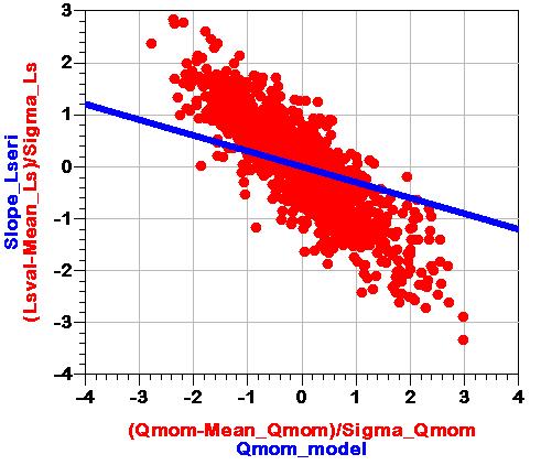
2 Overview Above 00Hz fmax by advanced CMOS technology is a driving force to realize millimeter-wave CMOS chips. Accurate/Automated 60Hz Measurement is needed to find a devices nature. Environmental-sensitive measurement and large local variation made modeling work very difficult. PVT model linking process and SPICE : a OAL of this work. Accurate Probing Control 3As Automatic Measurements Accurate PVT Model 35.0 L M H 34.5 ) B d ( 34.0 p Itotal(A)
3 Contents : :Demonstration of stable S-parameter automated measurement at 60 Hz. : Demonstration of simple PVT model for 60Hz region. -MOSFET - MOM Capacitor 3
4 Accurate Probing Control Skating Control: Reflects stability of Measurement data. Adjacent S-PAD: used to check stability check. Hz~67Hz/Hz De-embedding check: But How often? Pitch 50um 65nm RF-CMOS inch wafer 30 Dies 4


5 Automatic Measurement Auto Measurement: Cascade Elite300TM Precise wafer alignment into 3 dimensions And X/Y/Z directional control of prove skating. Auto Data processing:ic-cap Wafer Pro /Data Pro Keep man-power away from time consuming S-parameter measurements. Easy data visualization (ex. Histogram, correlation Matrices) 5

6 Result of Stability Check (Hz~67Hz) S S 60Hz 60Hz S S 60Hz 60Hz /4/03 43 min 6


7 Statistical summary of used sample at 60Hz Small sigma indicates the stability of the system. Stable probing contact S S Mean=-9.86dB Sigma=0.5dB Mean=-0.98dB Sigma=0.08dB 7

, Cds MOMCAP (M~M5 Stacked) L=0um, NF=0")
8 NMOSFET Lg=50nm, Wg=40um (=um x 40Fingers x 3 Blocks) Measurement condition :Id=50uA/um Vd=0.6V Vg=Vth0.3V Hz~67Hz/Hz FOM at 60Hz Accurate PVT model ft, fmax, gm, gds, Rg, Cgd(s), Cds MOMCAP (M~M5 Stacked) L=0um, NF=0 Hz~69Hz/Hz W L Spacing NF 8
9 Auto measurement results of Mom CAP S S 30 60Hz 60Hz S 60Hz S 60Hz Stable measurement 9


10 Frequency dispersion of equivalent circuit parameters CS RS 30 60Hz 60Hz Q CSUB 0

11 Auto measurement results of NMOS Vd=0.6V Vg~Vth0.4V DC 30

12 Auto measurement results of NMOS RF S S 30 60Hz 60Hz S 60Hz S 60Hz 90min


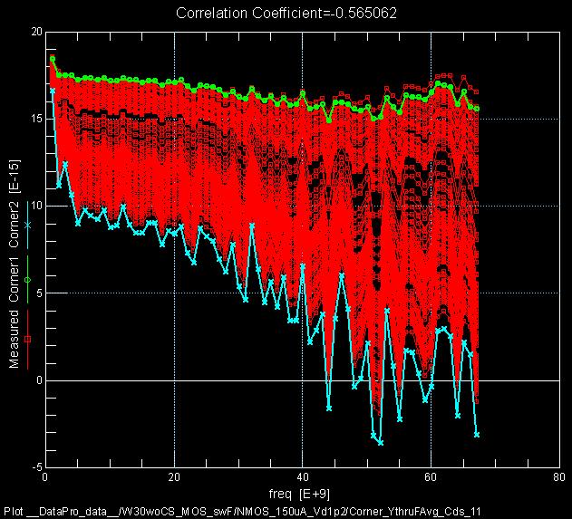

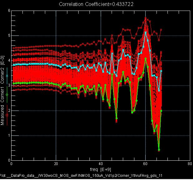
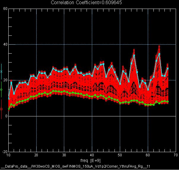
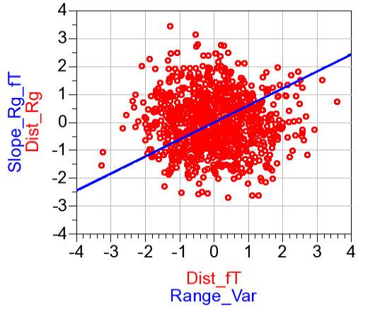
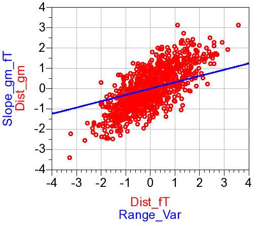
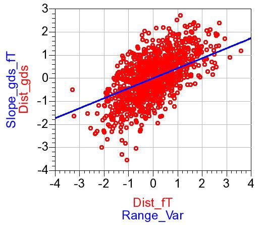
13 Frequency dependence of MOSFETs parameters fmax ft Cgd 30 Cds Rg gm gds Distribution are frequency dependent 3
14 Measure of components from y-parameters Y Y Y Y C = ω m C ω DS CS R R ω C ω D R CD C C C R gd ds gs jωc C C ( C D C m ) jω( C D C m ) ( C C C C C C ) jω( C C ) R = CB Im jωc Re Im BD D ( Y ) ( Y ) Y Y = Im = Im ( Y Y ) ( Y Y ) D D m g g m ds BD D Y Y = Re = Re ( Y Y ) Starting point the formula (.7a~.7d) : Christian C.Enz, Eric A. Vittoz, Charge-based MOS Transistor Modeling Wiley


15 Inter-wafer distributions of 60Hz fmax and Rg. fmax Rg High Low 5
16 Accurate PVT Model Challenges oal: give designers a direct insight of the process fluctuation risk on their circuit. Approach: Formulate the SPICE model parameters distribution via physical parameters Conventional Proposed model Circuit Performance VTH0 Circuit Performance Dot=Measurement ateoxide Thickness Channel Implantation Solid=Model 6
17 PDK Implementation toxe =Tox_par*(T_oxN/T_oxN0) toxp =Tox_par*(T_oxN/T_oxN0) toxm =Tox_par*(T_oxN/T_oxN0) ndep =Ndep0_p*(N_depN/N_depN0) vth0 =VTH0_p * KN_VTH0 k =K_p * KN_AMMA u0 =mu0_p * KN_vsat vsat =vsat_p * KN_vsat nfactor =nfact_p Model *KN_Nfactor Card pclm =pclm_p*kn_cml pdiblc =pdiblc_p * KN_CML pdiblc =pdiblc_p*kn_cml rdsw =rdsw_p * KN_RDSW lint =lint_p* KN_LINT wint =wint_p * KN_WINT cgso =cgso_p *KN_LOV cgdo =cgdo_p *KN_LOV cgbo =cgb0_p *KN_CB cjs =cjs_p *KN_cjsi0 cjsws =cjsws_p*kn_cjsi0 pbs =pbs_p*kn_vdsi0 N_depN =.7e7 T_oxN =.39e-7 LCORR_PERCENT_N=e-3 WCORR_PERCENT_N=e-3 rho_rate=0 statistics { process { vary N_depN dist=gauss std=aa percent=yes vary T_oxN dist=gauss std=bb percent=yes vary LCORR_PERCENT_N dist=gauss std=cc percent=yes vary WCORR_PERCENT_N dist=gauss std=dd percent=yes vary rho_rate dist=gauss std=ee percent=yes } } Monte Carlo Declaration Ndep /- 6% T_ox /- 6% LCORR /- 0% WCORR /- 5% R /- % Thick_Metal /- 0% 7
18 Overview of Model structure (Front-END) LINT WINT DLC Length of ate-s/d overlap region R ate resistance U0,VSAT Low field mobility, Saturated velocity CJ Junction Capacitancce N _ dep CJ = CJ BSIM N _ dep0 Deviation ( PB ) PB0 PB PB0 = N _ j N _ dep ln N _ i N _ j N _ dep0 ln N _ i 8
19 µ U0,VSAT i U0 Drift Mobility [cm/v-s] = U0 BSIM Carrier mobility vs. channel impurity concentration µ u u i µ max min l ( Ndep ) = µ min α α Ndep ( Ndep ) ( Ndep 0) i ref Hole Modulation N N.0E4.0E5.0E6.0E7.0E8.0E9 Impurity Concentration [cm-3] µ ref Ndep Electron Parameter A-As P B µ max (cm V - s - ) µ min (cm V - s - ) µ l (cm V - s - ) N ref (cm -3 ) 9.68E6 9.0E6.3E7 N ref (cm -3 ) 3.43E0 3.4E0 6.0E0 α α Formula for minority carriers. D.B.M. Klaassen,, A Unified Mobility Model for Device Simulation-I. Model Equations and Concentration Dependence, Solid-State Electronics Vol.35, No.7, pp , 99.. D.B.M. Klaassen,, A Unified Mobility Model for Device Simulation-II. Temperature Dependence of Carrier Mobility and Lifetime, Solid-State Electronics Vol.35, No.7, pp , 99. 9
20 0 ( ) ( ) ( ) = = = = = ]. [ n n n n L L n n L V I n n L V I n n L V I W I L Cgb Cgsi V I I Cox L W Cgdi Cgsi gm Cgd Cgs gm F T C T C T C T C C Ti µ µ µ µ π µ π µ π π Formulation of ft fluctuation via DLC N (Slope) factor DLC Offset arelength Mobilty LCORR = BSIM DLC DLC ( ) ( ) Ndep 0 u Ndep u i i L L L corr 0 0 n n n n. David M.Binkeley,, Tradeoffs and optimization in Analog CMOS Circuit Design, Wiley

21 Overview of Model structure (Back-END) ThickMetal_INT ThickMetal_INT Dist_INT ThickMetal_INT Dist_INT Dist_INT ThickMetal_INT Dist_LOC_INT ThickMetal_LOC CS0 CD0 Dist_SUB_LOC Csub Rsub SUB
 eps _ l Dist_SUB_L OC Dist_SUB_L OC 3 ( L W NF ) eps _ l Dist_INT Dist_INT Dist_INT Dist_INT Lateral C vertical = 8.854e = 8.")
22 The formulae of capacitance CS Vertical CDO CSO C vertical = 8.854e = 8.854e ( L W NF ) eps _ l Dist_SUB_L OC Dist_SUB_L OC 3 ( L W NF ) eps _ l Dist_INT Dist_INT Dist_INT Dist_INT Lateral C vertical = 8.854e = 8.854e ( L W ) eps _ w ( NF ) ThickMetal _ LOC ThickMetal _ INT ( L W NF ) eps _ w 3 ThickMetal _ LOC Spacing Spacing ThickMetal _ INT ThickMetal _ INT Spacing Spacing Spacing ThickMetal _ INT Spacing
23 Model Validation MOSFET 3
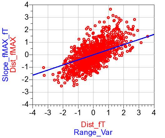


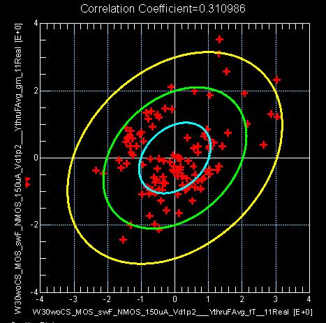
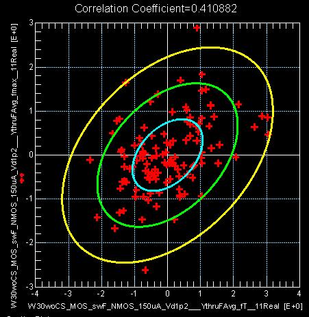

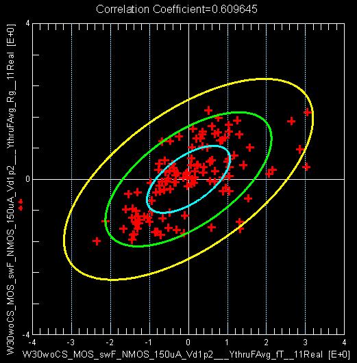
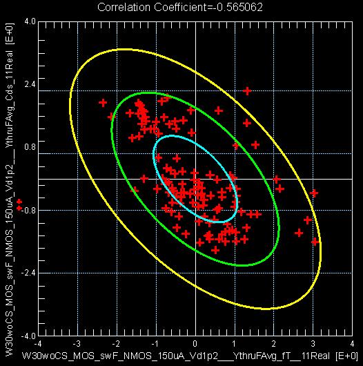

24 Measurement vs. Simulation correlation - fmax Rg fmax Rg Sigma ft Sigma ft Cgd Cds Cgd Cds Sigma ft Sigma ft gm 0.3 gds 0.43 gm gds Sigma ft Sigma ft ft : principle component 4
25 Model Validation MOM CAP 5


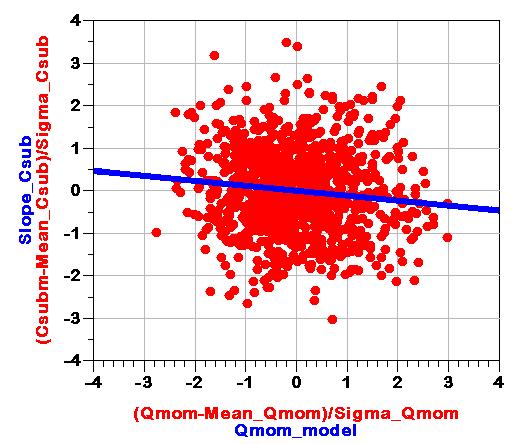


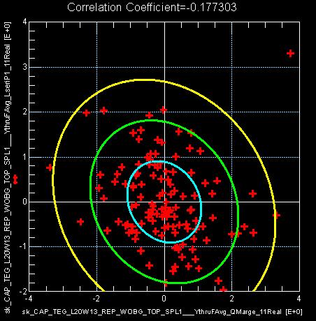

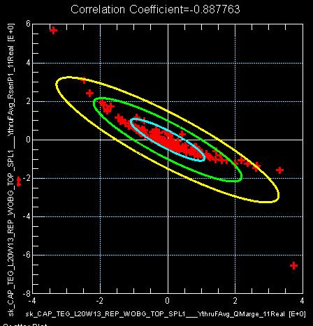
26 Measurement vs. Simulation Correlation from measurement Cs Ls Cs Ls Rs Rsub Rs Rsub Csub -0.3 Csub Q: principle component 6
27 Conclusion Automated 60Hz auto measurement. Thanks to the up-to-date hardware and data processing, we could capture the fluctuation of CMOS technology. Stability in the measurement system used in this work is kept good condition. It sensed that the deviation of MOSFET performance becomes larger as the operating frequency increases. Statistical modeling Our simplified PVT model can provide with reasonable estimation of intra-wafer variation at 60Hz. 7

28 8
RF CMOS Compact modelling technologies past and future
 RF C Compact modelling technologies past and future adayuki Yoshitomi sadayuki.yoshitomi@toshiba.co.jp Dedicated to - 2018 Q3 Meeting Toshiba Memory Corporation Contents 01 Background 02 RF High Volume
(S&S ) PMOS: holes flow from Source to Drain. from Source to Drain. W.-Y. Choi. Electronic Circuits 2 (09/1)
 PMOS: holes flow from Source to Drain. from Source to Drain. W.-Y. Choi. Electronic Circuits 2 (09/1)") (S&S 4.1 4.3) NMOS: electrons flow from Source to Drain PMOS: holes flow from Source to Drain In cut-off ( v < V ), i = 0 GS t D NMOS I-V Characteristics In triode, ( v > V but v v v ) GS t DS GS T W 1
(S&S 4.1 4.3) NMOS: electrons flow from Source to Drain PMOS: holes flow from Source to Drain In cut-off ( v < V ), i = 0 GS t D NMOS I-V Characteristics In triode, ( v > V but v v v ) GS t DS GS T W 1
The Devices. Devices
 The The MOS Transistor Gate Oxyde Gate Source n+ Polysilicon Drain n+ Field-Oxyde (SiO 2 ) p-substrate p+ stopper Bulk Contact CROSS-SECTION of NMOS Transistor Cross-Section of CMOS Technology MOS transistors
ESE 570: Digital Integrated Circuits and VLSI Fundamentals
 ESE 570: Digital Integrated Circuits and VLSI Fundamentals Lec 6: January 30, 2018 MOS Operating Regions, pt. 2 Lecture Outline! Operating Regions (review) " Subthreshold " Resistive " Saturation! Intro.
EKV MOS Transistor Modelling & RF Application
 HP-RF MOS Modelling Workshop, Munich, February 15-16, 1999 EKV MOS Transistor Modelling & RF Application Matthias Bucher, Wladek Grabinski Electronics Laboratory (LEG) Swiss Federal Institute of Technology,
EE 560 MOS TRANSISTOR THEORY PART 2. Kenneth R. Laker, University of Pennsylvania
 1 EE 560 MOS TRANSISTOR THEORY PART nmos TRANSISTOR IN LINEAR REGION V S = 0 V G > V T0 channel SiO V D = small 4 C GC C BC substrate depletion region or bulk B p nmos TRANSISTOR AT EDGE OF SATURATION
Sadayuki Yoshitomi. Semiconductor Company 2007/01/25
 Sadayuki Yoshitomi. Semiconductor Company Sadayuki.yoshitomi@toshiba.co.jp Copyright 2006, Toshiba Corporation. ASP-DAC 2007 . Make the best of Electro-Magnetic (EM) simulation. Is EM simulator applicable
Lecture 37: Frequency response. Context
 EECS 05 Spring 004, Lecture 37 Lecture 37: Frequency response Prof J. S. Smith EECS 05 Spring 004, Lecture 37 Context We will figure out more of the design parameters for the amplifier we looked at in
EE105 Fall 2014 Microelectronic Devices and Circuits. NMOS Transistor Capacitances: Saturation Region
 EE105 Fall 014 Microelectronic Devices and Circuits Prof. Ming C. Wu wu@eecs.berkeley.edu 511 Sutardja Dai Hall (SDH) 1 NMOS Transistor Capacitances: Saturation Region Drain no longer connected to channel
ECE 342 Electronic Circuits. 3. MOS Transistors
 ECE 342 Electronic Circuits 3. MOS Transistors Jose E. Schutt-Aine Electrical & Computer Engineering University of Illinois jschutt@emlab.uiuc.edu 1 NMOS Transistor Typically L = 0.1 to 3 m, W = 0.2 to
APPENDIX D: Binning BSIM3v3 Parameters
 APPENDIX D: Binning BSIM3v3 Parameters Below is a list of all BSIM3v3 model parameters which can or cannot be binned. All model parameters which can be binned follow the following implementation: P L P
EE 330 Homework 5 Spring 2017 (This assignment will not be collected or graded)
") EE 330 Homework 5 Spring 2017 (This assignment will not be collected or graded) Assume the CMOS process is characterized by model parameters V TH =1V and µc OX =100µA/V 2. If any other model parameters
EE 330 Homework 5 Spring 2017 (This assignment will not be collected or graded) Assume the CMOS process is characterized by model parameters V TH =1V and µc OX =100µA/V 2. If any other model parameters
EE 240B Spring Advanced Analog Integrated Circuits Lecture 2: MOS Transistor Models. Elad Alon Dept. of EECS
 EE 240B Spring 2018 Advanced Analog Integrated Circuits Lecture 2: MOS Transistor Models Elad Alon Dept. of EECS Square Law Model? Assumptions made to come up with this model: Charge density determined
APPENDIX A: Parameter List
 APPENDIX A: Parameter List A.1 BSIM3v3 Model Control Parameters none level BSIMv3 model selector 8 none Mobmod mobmod Mobility model selector 1 none Capmod capmod Flag for the short channel 1 none capacitance
University of Pennsylvania Department of Electrical Engineering. ESE 570 Midterm Exam March 14, 2013 FORMULAS AND DATA
 University of Pennsylvania Department of Electrical Engineering ESE 570 Midterm Exam March 4, 03 FORMULAS AND DATA. PHYSICAL CONSTANTS: n i = intrinsic concentration undoped) silicon =.45 x 0 0 cm -3 @
APPENDIX A: Parameter List
 APPENDIX A: Parameter List A.1 BSIM3v3 Model Control Parameters none level BSIMv3 model selector 8 none Mobmod mobmod Mobility model selector 1 none Capmod capmod Flag for the short channel 2 none capacitance
ESE 570: Digital Integrated Circuits and VLSI Fundamentals
 ESE 570: Digital Integrated Circuits and VLSI Fundamentals Lec 7: February 4, 2016 MOS SPICE Models, MOS Parasitic Details Lecture Outline! MOS Capacitances " Extrinsic " Intrinsic! Lumped Capacitance
Frequency Response Prof. Ali M. Niknejad Prof. Rikky Muller
 EECS 105 Spring 2017, Module 4 Frequency Response Prof. Ali M. Niknejad Department of EECS Announcements l HW9 due on Friday 2 Review: CD with Current Mirror 3 Review: CD with Current Mirror 4 Review:
Lecture 3: CMOS Transistor Theory
 Lecture 3: CMOS Transistor Theory Outline Introduction MOS Capacitor nmos I-V Characteristics pmos I-V Characteristics Gate and Diffusion Capacitance 2 Introduction So far, we have treated transistors
ASM-HEMT Model for GaN RF and Power Electronic Applications: Overview and Extraction
 ASM-HEMT Model for GaN RF and Power Electronic Applications: Overview and Extraction June 27, 2016 Sheikh Aamir Ahsan Sudip Ghosh Yogesh Singh Chauhan IIT Kanpur Sourabh Khandelwal UC Berkeley MA Long
Multistage Amplifier Frequency Response
 Multistage Amplifier Frequency Response * Summary of frequency response of single-stages: CE/CS: suffers from Miller effect CC/CD: wideband -- see Section 0.5 CB/CG: wideband -- see Section 0.6 (wideband
ECE 546 Lecture 10 MOS Transistors
 ECE 546 Lecture 10 MOS Transistors Spring 2018 Jose E. Schutt-Aine Electrical & Computer Engineering University of Illinois jesa@illinois.edu NMOS Transistor NMOS Transistor N-Channel MOSFET Built on p-type
! MOS Capacitances. " Extrinsic. " Intrinsic. ! Lumped Capacitance Model. ! First Order Capacitor Summary. ! Capacitance Implications
 ESE 570: Digital Integrated Circuits and VLSI Fundamentals Lec 7: February, 07 MOS SPICE Models, MOS Parasitic Details Lecture Outline! MOS Capacitances " Extrinsic " Intrinsic! Lumped Capacitance Model!
Lecture 4: CMOS Transistor Theory
 Introduction to CMOS VLSI Design Lecture 4: CMOS Transistor Theory David Harris, Harvey Mudd College Kartik Mohanram and Steven Levitan University of Pittsburgh Outline q Introduction q MOS Capacitor q
Simple and accurate modeling of the 3D structural variations in FinFETs
 Simple and accurate modeling of the 3D structural variations in FinFETs Donghu Kim Electrical Engineering Program Graduate school of UNIST 2013 Simple and accurate modeling of the 3D structural variations
The Miller Approximation
 The Miller Approximation The exact analysis is not particularly helpful for gaining insight into the frequency response... consider the effect of C µ on the input only I t C µ V t g m V t R'out = r o r
Device Models (PN Diode, MOSFET )
") Device Models (PN Diode, MOSFET ) Instructor: Steven P. Levitan steve@ece.pitt.edu TA: Gayatri Mehta, José Martínez Book: Digital Integrated Circuits: A Design Perspective; Jan Rabaey Lab Notes: Handed
Device Models (PN Diode, MOSFET ) Instructor: Steven P. Levitan steve@ece.pitt.edu TA: Gayatri Mehta, José Martínez Book: Digital Integrated Circuits: A Design Perspective; Jan Rabaey Lab Notes: Handed
APPENDIX D: Model Parameter Binning
 APPENDIX D: Model Parameter Binning Below is the information on parameter binning regarding which model parameters can or cannot be binned. All those parameters which can be binned follow this implementation:
The Devices. Digital Integrated Circuits A Design Perspective. Jan M. Rabaey Anantha Chandrakasan Borivoje Nikolic. July 30, 2002
 Digital Integrated Circuits A Design Perspective Jan M. Rabaey Anantha Chandrakasan Borivoje Nikolic The Devices July 30, 2002 Goal of this chapter Present intuitive understanding of device operation Introduction
The Devices: MOS Transistors
 The Devices: MOS Transistors References: Semiconductor Device Fundamentals, R. F. Pierret, Addison-Wesley Digital Integrated Circuits: A Design Perspective, J. Rabaey et.al. Prentice Hall NMOS Transistor
Circuits. L2: MOS Models-2 (1 st Aug. 2013) B. Mazhari Dept. of EE, IIT Kanpur. B. Mazhari, IITK. G-Number
 B. Mazhari Dept. of EE, IIT Kanpur. B. Mazhari, IITK. G-Number") EE610: CMOS Analog Circuits L: MOS Models- (1 st Aug. 013) B. Mazhari Dept. of EE, IIT Kanpur 3 NMOS Models MOS MODEL Above Threshold Subthreshold ( GS > TN ) ( GS < TN ) Saturation ti Ti Triode ( DS >
EE610: CMOS Analog Circuits L: MOS Models- (1 st Aug. 013) B. Mazhari Dept. of EE, IIT Kanpur 3 NMOS Models MOS MODEL Above Threshold Subthreshold ( GS > TN ) ( GS < TN ) Saturation ti Ti Triode ( DS >
Study of MOSFET circuit
 ECE 570 Computer Aided Engineering for Integrated Circuits IC 752 - E Simulation Assignment No. 3 - Due: Oct. 30 (Th.), 2003 Study of MOSFET circuit Simulate the basic circuit of CMOS shift register shown
Operation and Modeling of. The MOS Transistor. Second Edition. Yannis Tsividis Columbia University. New York Oxford OXFORD UNIVERSITY PRESS
 Operation and Modeling of The MOS Transistor Second Edition Yannis Tsividis Columbia University New York Oxford OXFORD UNIVERSITY PRESS CONTENTS Chapter 1 l.l 1.2 1.3 1.4 1.5 1.6 1.7 Chapter 2 2.1 2.2
Integrated Circuit Design: OTA in 0.5µm Technology
 Integrated Circuit Design: OTA in 0.5µm Technology Omar X. Avelar, Omar de la Mora & Diego I. Romero INTEGRATED CIRCUITS DESIGN (ESI108A) Instituto Tecnológico y de Estudios Superiores de Occidente (ITESO)
EEC 118 Lecture #2: MOSFET Structure and Basic Operation. Rajeevan Amirtharajah University of California, Davis Jeff Parkhurst Intel Corporation
 EEC 118 Lecture #2: MOSFET Structure and Basic Operation Rajeevan Amirtharajah University of California, Davis Jeff Parkhurst Intel Corporation Announcements Lab 1 this week, report due next week Bring
MOSFET: Introduction
 E&CE 437 Integrated VLSI Systems MOS Transistor 1 of 30 MOSFET: Introduction Metal oxide semiconductor field effect transistor (MOSFET) or MOS is widely used for implementing digital designs Its major
EE 330 Homework 5 Fall 2018 (This assignment is due Wednesday Sept 19 at 12:00 noon)
") EE 330 Homework 5 Fall 2018 (This assignment is due Wednesday Sept 19 at 12:00 noon) Assume the CMOS process is characterized by model parameters VTH=1V and µcox=100µa/v 2. If any other model parameters
EE 330 Homework 5 Fall 2018 (This assignment is due Wednesday Sept 19 at 12:00 noon) Assume the CMOS process is characterized by model parameters VTH=1V and µcox=100µa/v 2. If any other model parameters
ECEN474/704: (Analog) VLSI Circuit Design Spring 2018
 VLSI Circuit Design Spring 2018") ECEN474/704: (Analog) SI Circuit Design Spring 2018 ecture 2: MOS ransistor Modeling Sam Palermo Analog & Mixed-Signal Center exas A&M University Announcements If you haven t already, turn in your 0.18um
ECEN474/704: (Analog) SI Circuit Design Spring 2018 ecture 2: MOS ransistor Modeling Sam Palermo Analog & Mixed-Signal Center exas A&M University Announcements If you haven t already, turn in your 0.18um
Different Strategies for Statistical Compact Modeling MOS-AK Dresden
 Different Strategies for Statistical Compact Modeling MOS-AK Dresden 18.3. Dr. Marat Yakupov (MunEDA) Dr. Michael Pronath (MunEDA) Dr. Elmar Gondro (Infineon Technologies) Overview Process Manufacturing
RFIC2017 MO2B-2. A Simplified CMOS FET Model using Surface Potential Equations For Inter-modulation Simulations of Passive-Mixer-Like Circuits
 A Simplified CMOS FET Model using Surface Potential Equations For Inter-modulation Simulations of Passive-Mixer-Like Circuits M. Baraani Dastjerdi and H. Krishnaswamy CoSMIC Lab, Columbia University, New
ECE 497 JS Lecture - 12 Device Technologies
 ECE 497 JS Lecture - 12 Device Technologies Spring 2004 Jose E. Schutt-Aine Electrical & Computer Engineering University of Illinois jose@emlab.uiuc.edu 1 NMOS Transistor 2 ρ Source channel charge density
Microelectronics Part 1: Main CMOS circuits design rules
 GBM8320 Dispositifs Médicaux telligents Microelectronics Part 1: Main CMOS circuits design rules Mohamad Sawan et al. Laboratoire de neurotechnologies Polystim! http://www.cours.polymtl.ca/gbm8320/! med-amine.miled@polymtl.ca!
The Devices. Jan M. Rabaey
 The Devices Jan M. Rabaey Goal of this chapter Present intuitive understanding of device operation Introduction of basic device equations Introduction of models for manual analysis Introduction of models
MOS Transistor Properties Review
 MOS Transistor Properties Review 1 VLSI Chip Manufacturing Process Photolithography: transfer of mask patterns to the chip Diffusion or ion implantation: selective doping of Si substrate Oxidation: SiO
ESE 570 MOS TRANSISTOR THEORY Part 2
 ESE 570 MOS TRANSISTOR THEORY Part 2 GCA (gradual channel approximation) MOS Transistor Model Strong Inversion Operation CMOS = NMOS + PMOS 2 TwoTerminal MOS Capacitor > nmos Transistor VGS
6.012 Electronic Devices and Circuits Spring 2005
 6.012 Electronic Devices and Circuits Spring 2005 May 16, 2005 Final Exam (200 points) -OPEN BOOK- Problem NAME RECITATION TIME 1 2 3 4 5 Total General guidelines (please read carefully before starting):
MOSFET Model with Simple Extraction Procedures, Suitable for Sensitive Analog Simulations
 ROMANIAN JOURNAL OF INFORMATION SCIENCE AND TECHNOLOGY Volume 10, Number 2, 2007, 189 197 MOSFET Model with Simple Extraction Procedures, Suitable for Sensitive Analog Simulations S. EFTIMIE 1, ALEX. RUSU
Philips Research apple PHILIPS
 c Electronics N.V. 1997 Modelling Compact of Submicron CMOS D.B.M. Klaassen Research Laboratories The Netherlands Eindhoven, contents accuracy and benchmark criteria new applications í RF modelling advanced
Introduction and Background
 Analog CMOS Integrated Circuit Design Introduction and Background Dr. Jawdat Abu-Taha Department of Electrical and Computer Engineering Islamic University of Gaza jtaha@iugaza.edu.ps 1 Marking Assignments
ECE 342 Electronic Circuits. Lecture 6 MOS Transistors
 ECE 342 Electronic Circuits Lecture 6 MOS Transistors Jose E. Schutt-Aine Electrical & Computer Engineering University of Illinois jesa@illinois.edu 1 NMOS Transistor Typically L = 0.1 to 3 m, W = 0.2
Lecture 15: MOS Transistor models: Body effects, SPICE models. Context. In the last lecture, we discussed the modes of operation of a MOS FET:
 Lecture 15: MOS Transistor models: Body effects, SPICE models Context In the last lecture, we discussed the modes of operation of a MOS FET: oltage controlled resistor model I- curve (Square-Law Model)
CMOS Analog Circuits
 CMOS Analog Circuits L6: Common Source Amplifier-1 (.8.13) B. Mazhari Dept. of EE, IIT Kanpur 19 Problem statement : Design an amplifier which has the following characteristics: + CC O in R L - CC A 100
Chapter 9 Frequency Response. PART C: High Frequency Response
 Chapter 9 Frequency Response PART C: High Frequency Response Discrete Common Source (CS) Amplifier Goal: find high cut-off frequency, f H 2 f H is dependent on internal capacitances V o Load Resistance
The PSP compact MOSFET model An update
 The PSP compact MOSFET model An update Gert-Jan Smit, Andries Scholten, D.B.M. Klaassen NXP Semiconductors Ronald van Langevelde Philips Research Europe Gennady Gildenblat, Weimin Wu, Xin Li, Amit Jha,
Transfer Gate and Dynamic Logic Dr. Lynn Fuller Webpage:
 ROCHESTER INSTITUTE OF TECHNOLOGY MICROELECTRONIC ENGINEERING Transfer Gate and Dynamic Logic Dr. Lynn Fuller Webpage: http://people.rit.edu/lffeee 82 Lomb Memorial Drive Rochester, NY 14623-5604 Tel (585)
MOSFET Capacitance Model
 MOSFET Capacitance Model So far we discussed the MOSFET DC models. In real circuit operation, the device operates under time varying terminal voltages and the device operation can be described by: 1 small
MOS Transistor Theory
 CHAPTER 3 MOS Transistor Theory Outline 2 1. Introduction 2. Ideal I-V Characteristics 3. Nonideal I-V Effects 4. C-V Characteristics 5. DC Transfer Characteristics 6. Switch-level RC Delay Models MOS
Fundamentals of the Metal Oxide Semiconductor Field-Effect Transistor
 Triode Working FET Fundamentals of the Metal Oxide Semiconductor Field-Effect Transistor The characteristics of energy bands as a function of applied voltage. Surface inversion. The expression for the
Charge-Storage Elements: Base-Charging Capacitance C b
 Charge-Storage Elements: Base-Charging Capacitance C b * Minority electrons are stored in the base -- this charge q NB is a function of the base-emitter voltage * base is still neutral... majority carriers
LEVEL 61 RPI a-si TFT Model
 LEVEL 61 RPI a-si TFT Model Star-Hspice LEVEL 61 is an AIM-SPICE MOS15 amorphous silicon (a-si) thin-film transistor (TFT) model. Model Features AIM-SPICE MOS15 a-si TFT model features include: Modified
Common Drain Stage (Source Follower) Claudio Talarico, Gonzaga University
 Claudio Talarico, Gonzaga University") Common Drain Stage (Source Follower) Claudio Talarico, Gonzaga University Common Drain Stage v gs v i - v o V DD v bs - v o R S Vv IN i v i G C gd C+C gd gb B&D v s vv OUT o + V S I B R L C L v gs - C
Common Drain Stage (Source Follower) Claudio Talarico, Gonzaga University Common Drain Stage v gs v i - v o V DD v bs - v o R S Vv IN i v i G C gd C+C gd gb B&D v s vv OUT o + V S I B R L C L v gs - C
EE5311- Digital IC Design
 EE5311- Digital IC Design Module 1 - The Transistor Janakiraman V Assistant Professor Department of Electrical Engineering Indian Institute of Technology Madras Chennai October 28, 2017 Janakiraman, IITM
MOS Amplifiers Dr. Lynn Fuller Webpage:
 ROCHESTER INSTITUTE OF TECHNOLOGY MICROELECTRONIC ENGINEERING Dr. Lynn Fuller Webpage: http://people.rit.edu/lffeee 82 Lomb Memorial Drive Rochester, NY 14623-5604 Email: Lynn.Fuller@rit.edu Department
EE105 Fall 2015 Microelectronic Devices and Circuits Frequency Response. Prof. Ming C. Wu 511 Sutardja Dai Hall (SDH)
") EE05 Fall 205 Microelectronic Devices and Circuits Frequency Response Prof. Ming C. Wu wu@eecs.berkeley.edu 5 Sutardja Dai Hall (SDH) Amplifier Frequency Response: Lower and Upper Cutoff Frequency Midband
EE05 Fall 205 Microelectronic Devices and Circuits Frequency Response Prof. Ming C. Wu wu@eecs.berkeley.edu 5 Sutardja Dai Hall (SDH) Amplifier Frequency Response: Lower and Upper Cutoff Frequency Midband
Lecture 23 - Frequency Resp onse of Amplifiers (I) Common-Source Amplifier. May 6, 2003
 Common-Source Amplifier. May 6, 2003") 6.0 Microelectronic Devices and Circuits Spring 003 Lecture 3 Lecture 3 Frequency Resp onse of Amplifiers (I) CommonSource Amplifier May 6, 003 Contents:. Intro duction. Intrinsic frequency resp onse of
6.0 Microelectronic Devices and Circuits Spring 003 Lecture 3 Lecture 3 Frequency Resp onse of Amplifiers (I) CommonSource Amplifier May 6, 003 Contents:. Intro duction. Intrinsic frequency resp onse of
EE 330 Lecture 16. Devices in Semiconductor Processes. MOS Transistors
 EE 330 Lecture 16 Devices in Semiconductor Processes MOS Transistors Review from Last Time Model Summary I D I V DS V S I B V BS = 0 0 VS VT W VDS ID = μcox VS VT VDS VS V VDS VS VT L T < W μc ( V V )
EE105 Fall 2014 Microelectronic Devices and Circuits
 EE05 Fall 204 Microelectronic Devices and Circuits Prof. Ming C. Wu wu@eecs.berkeley.edu 5 Sutardja Dai Hall (SDH) Terminal Gain and I/O Resistances of BJT Amplifiers Emitter (CE) Collector (CC) Base (CB)
ID # NAME. EE-255 EXAM 3 April 7, Instructor (circle one) Ogborn Lundstrom
 Ogborn Lundstrom") ID # NAME EE-255 EXAM 3 April 7, 1998 Instructor (circle one) Ogborn Lundstrom This exam consists of 20 multiple choice questions. Record all answers on this page, but you must turn in the entire exam.
ID # NAME EE-255 EXAM 3 April 7, 1998 Instructor (circle one) Ogborn Lundstrom This exam consists of 20 multiple choice questions. Record all answers on this page, but you must turn in the entire exam.
The HV-EKV MOSFET Model
 The HV-EKV MOSFET Model Ecole Polytechnique Fédérale de Lausanne (EPFL), Switzerland EPFL Team Yogesh Singh Chauhan, Costin Anghel, Francois Krummenacher, Adrian Mihai Ionescu and Michel Declercq CMC Meeting,
Chapter 4 Field-Effect Transistors
 Chapter 4 Field-Effect Transistors Microelectronic Circuit Design Richard C. Jaeger Travis N. Blalock 5/5/11 Chap 4-1 Chapter Goals Describe operation of MOSFETs. Define FET characteristics in operation
Practice 7: CMOS Capacitance
 Practice 7: CMOS Capacitance Digital Electronic Circuits Semester A 2012 MOSFET Capacitances MOSFET Capacitance Components 3 Gate to Channel Capacitance In general, the gate capacitance is similar to a
MOS Transistor Theory
 MOS Transistor Theory So far, we have viewed a MOS transistor as an ideal switch (digital operation) Reality: less than ideal EE 261 Krish Chakrabarty 1 Introduction So far, we have treated transistors
MOS Transistor I-V Characteristics and Parasitics
 ECEN454 Digital Integrated Circuit Design MOS Transistor I-V Characteristics and Parasitics ECEN 454 Facts about Transistors So far, we have treated transistors as ideal switches An ON transistor passes
EE105 - Fall 2006 Microelectronic Devices and Circuits
 EE105 - Fall 2006 Microelectronic Devices and Circuits Prof. Jan M. Rabaey (jan@eecs) Lecture 7: MOS Transistor Some Administrative Issues Lab 2 this week Hw 2 due on We Hw 3 will be posted same day MIDTERM
Page 1 of (2 pts) What is the purpose of the keeper transistor in a dynamic logic gate?
 What is the purpose of the keeper transistor in a dynamic logic gate?") Page 1 of 6 EE 434 Exam 2 Fall 2004 Name Instructions: nswer the following questions and solve the following problems. In problems relating to timing or delay calculations, assume you are working in a
Page 1 of 6 EE 434 Exam 2 Fall 2004 Name Instructions: nswer the following questions and solve the following problems. In problems relating to timing or delay calculations, assume you are working in a
Section 12: Intro to Devices
 Section 12: Intro to Devices Extensive reading materials on reserve, including Robert F. Pierret, Semiconductor Device Fundamentals EE143 Ali Javey Bond Model of Electrons and Holes Si Si Si Si Si Si Si
CHAPTER 3: TRANSISTOR MOSFET DR. PHAM NGUYEN THANH LOAN. Hà Nội, 9/24/2012
 1 CHAPTER 3: TRANSISTOR MOSFET DR. PHAM NGUYEN THANH LOAN Hà Nội, 9/24/2012 Chapter 3: MOSFET 2 Introduction Classifications JFET D-FET (Depletion MOS) MOSFET (Enhancement E-FET) DC biasing Small signal
USC-ISI. The MOSIS Service. BSIM3v3.1 Model. Parameters Extraction and Optimization. October 2000
 USC-ISI The MOSIS Service BSIM3v3.1 Model Parameters Extraction and Optimization October 000 Henok Abebe ance C.Tyree Table of Contents 1. Introduction and Motivation: -----------------------------------------------1.
Lecture 04 Review of MOSFET
 ECE 541/ME 541 Microelectronic Fabrication Techniques Lecture 04 Review of MOSFET Zheng Yang (ERF 3017, email: yangzhen@uic.edu) What is a Transistor? A Switch! An MOS Transistor V GS V T V GS S Ron D
Lecture 10 MOSFET (III) MOSFET Equivalent Circuit Models
 MOSFET Equivalent Circuit Models") Lecture 1 MOSFET (III) MOSFET Equivalent Circuit Models Outline Lowfrequency smallsignal equivalent circuit model Highfrequency smallsignal equivalent circuit model Reading Assignment: Howe and Sodini;
Lecture 1 MOSFET (III) MOSFET Equivalent Circuit Models Outline Lowfrequency smallsignal equivalent circuit model Highfrequency smallsignal equivalent circuit model Reading Assignment: Howe and Sodini;
ECEN474/704: (Analog) VLSI Circuit Design Spring 2018
 VLSI Circuit Design Spring 2018") ECEN474/704: (Analog) VLSI Circuit Design Spring 2018 Lecture 4: MOS ransistor Modeling Sam Palermo Analog & Mixed-Signal Center exas A&M University Agenda MOS ransistor Modeling MOS Spice Models MOS High-Order
ECEN474/704: (Analog) VLSI Circuit Design Spring 2018 Lecture 4: MOS ransistor Modeling Sam Palermo Analog & Mixed-Signal Center exas A&M University Agenda MOS ransistor Modeling MOS Spice Models MOS High-Order
EE105 - Fall 2005 Microelectronic Devices and Circuits
 EE105 - Fall 005 Microelectronic Devices and Circuits ecture 7 MOS Transistor Announcements Homework 3, due today Homework 4 due next week ab this week Reading: Chapter 4 1 ecture Material ast lecture
Workshop WMB. Noise Modeling
 Workshop WMB Noise Modeling Manfred Berroth, Markus Grözing, Stefan Heck, Alexander Bräckle University of Stuttgart, Germany WMB (IMS) Parameter Extraction Strategies For Compact Transistor Models IMS
ECE 546 Lecture 11 MOS Amplifiers
 ECE 546 Lecture MOS Amplifiers Spring 208 Jose E. Schutt-Aine Electrical & Computer Engineering University of Illinois jesa@illinois.edu ECE 546 Jose Schutt Aine Amplifiers Definitions Used to increase
Lecture 15 OUTLINE. MOSFET structure & operation (qualitative) Review of electrostatics The (N)MOS capacitor
 Review of electrostatics The (N)MOS capacitor") Lecture 15 OUTLINE MOSFET structure & operation (qualitative) Review of electrostatics The (N)MOS capacitor Electrostatics t ti Charge vs. voltage characteristic Reading: Chapter 6.1 6.2.1 EE105 Fall 2007
Lecture 15 OUTLINE MOSFET structure & operation (qualitative) Review of electrostatics The (N)MOS capacitor Electrostatics t ti Charge vs. voltage characteristic Reading: Chapter 6.1 6.2.1 EE105 Fall 2007
Effects of Scaling on Modeling of Analog RF MOS Devices
 Effects of Scaling on Modeling of Analog RF MOS Devices Y. Liu, S. Cao, T.-Y. Oh 1, B. Wu, O. Tornblad 2, R. Dutton Center for Integrated Systems, Stanford University 1 LG Electronics 2 Infineon Technologies
ECEN 326 Electronic Circuits
 ECEN 326 Electronic Circuits Frequency Response Dr. Aydın İlker Karşılayan Texas A&M University Department of Electrical and Computer Engineering High-Frequency Model BJT & MOS B or G r x C f C or D r
1/13/12 V DS. I d V GS. C ox ( = f (V GS ,V DS ,V SB = I D. + i d + I ΔV + I ΔV BS V BS. 19 January 2012
 /3/ 9 January 0 Study the linear model of MOS transistor around an operating point." MOS in saturation: V GS >V th and V S >V GS -V th " VGS vi - I d = I i d VS I d = µ n ( L V V γ Φ V Φ GS th0 F SB F
Lecture 12: MOSFET Devices
 Lecture 12: MOSFET Devices Gu-Yeon Wei Division of Engineering and Applied Sciences Harvard University guyeon@eecs.harvard.edu Wei 1 Overview Reading S&S: Chapter 5.1~5.4 Supplemental Reading Background
Thin Film Transistors (TFT)
") Thin Film Transistors (TFT) a-si TFT - α-si:h (Hydrogenated amorphous Si) deposited with a PECVD system (low temp. process) replaces the single crystal Si substrate. - Inverted staggered structure with
Thin Film Transistors (TFT) a-si TFT - α-si:h (Hydrogenated amorphous Si) deposited with a PECVD system (low temp. process) replaces the single crystal Si substrate. - Inverted staggered structure with
EECS240 Spring Today s Lecture. Lecture 2: CMOS Technology and Passive Devices. Lingkai Kong EECS. EE240 CMOS Technology
 EECS240 Spring 2013 Lecture 2: CMOS Technology and Passive Devices Lingkai Kong EECS Today s Lecture EE240 CMOS Technology Passive devices Motivation Resistors Capacitors (Inductors) Next time: MOS transistor
Integrated Circuits & Systems
 Federal University of Santa Catarina Center for Technology Computer Science & Electronics Engineering Integrated Circuits & Systems INE 5442 Lecture 10 MOSFET part 1 guntzel@inf.ufsc.br ual-well Trench-Isolated
Lecture 23: Negative Resistance Osc, Differential Osc, and VCOs
 EECS 142 Lecture 23: Negative Resistance Osc, Differential Osc, and VCOs Prof. Ali M. Niknejad University of California, Berkeley Copyright c 2005 by Ali M. Niknejad A. M. Niknejad University of California,
SUPPLEMENTARY INFORMATION
 doi:.38/nature09979 I. Graphene material growth and transistor fabrication Top-gated graphene RF transistors were fabricated based on chemical vapor deposition (CVD) grown graphene on copper (Cu). Cu foil
Lecture 23 Frequency Response of Amplifiers (I) Common Source Amplifier. December 1, 2005
 Common Source Amplifier. December 1, 2005") 6.02 Microelectronic Devices and Circuits Fall 2005 Lecture 23 Lecture 23 Frequency Response of Amplifiers (I) Common Source Amplifier December, 2005 Contents:. Introduction 2. Intrinsic frequency response
6.02 Microelectronic Devices and Circuits Fall 2005 Lecture 23 Lecture 23 Frequency Response of Amplifiers (I) Common Source Amplifier December, 2005 Contents:. Introduction 2. Intrinsic frequency response
CMPEN 411 VLSI Digital Circuits. Lecture 03: MOS Transistor
 CMPEN 411 VLSI Digital Circuits Lecture 03: MOS Transistor Kyusun Choi [Adapted from Rabaey s Digital Integrated Circuits, Second Edition, 2003 J. Rabaey, A. Chandrakasan, B. Nikolic] CMPEN 411 L03 S.1
P. R. Nelson 1 ECE418 - VLSI. Midterm Exam. Solutions
 P. R. Nelson 1 ECE418 - VLSI Midterm Exam Solutions 1. (8 points) Draw the cross-section view for A-A. The cross-section view is as shown below.. ( points) Can you tell which of the metal1 regions is the
Chapter 2 CMOS Transistor Theory. Jin-Fu Li Department of Electrical Engineering National Central University Jungli, Taiwan
 Chapter 2 CMOS Transistor Theory Jin-Fu Li Department of Electrical Engineering National Central University Jungli, Taiwan Outline Introduction MOS Device Design Equation Pass Transistor Jin-Fu Li, EE,
LECTURE 3 MOSFETS II. MOS SCALING What is Scaling?
 LECTURE 3 MOSFETS II Lecture 3 Goals* * Understand constant field and constant voltage scaling and their effects. Understand small geometry effects for MOS transistors and their implications modeling and