Section 12: Intro to Devices
|
|
|
- Sydney Pierce
- 5 years ago
- Views:
Transcription
1 Section 12: Intro to Devices Extensive reading materials on reserve, including Robert F. Pierret, Semiconductor Device Fundamentals EE143 Ali Javey
2 Bond Model of Electrons and Holes Si Si Si Si Si Si Si Si Si Silicon crystal in a two-dimensional representation. Si Si Si Si Si Si Si Si Si Si Si Si Si Si Si Si Si Si When an electron breaks loose and becomes a conduction electron, a hole is also created. EE143 Ali Javey
3 Semiconductors, Insulators, and Conductors E c E g=1.1 ev E c Ev E g= 9 ev E v Top of conduction band empty filled E c Si, Semiconductor SiO 2, insulator Conductor Totally filled bands and totally empty bands do not allow current flow. (Just as there is no motion of liquid in a totally filled or totally empty bottle.) Metal conduction band is half-filled. Semiconductors have lower E G s than insulators and can be doped EE143 Ali Javey
4 Dopants in Silicon Si Si Si Si Si Si Si As Si Si B Si Si Si Si Si Si Si As, a Group V element, introduces conduction electrons and creates N-type silicon, and is called a donor. B, a Group III element, introduces holes and creates P-type silicon, and is called an acceptor. EE143 Ali Javey
5 Types of charges in semiconductors Hole Electron Mobile Charge Carriers they contribute to current flow with electric field is applied. Ionized Donor Ionized Acceptor Immobile Charges they DO NOT contribute to current flow with electric field is applied. However, they affect the local electric field EE143 Ali Javey
6 Fermi Function The Probability of an Energy State Being Occupied by an Electron f ( E) = ( E E ) / kt E 1+ e 1 f E f is called the Fermi energy or the Fermi level. Boltzmann approximation: f ( E E ) kt f ( E) e E E f >> kt E f E f E f + 3kT + 2kT E f + kt ( E E f ) kt f ( E) e f ( E ) kt E ( E) 1 e f E E f << kt E f E f kt E f 2kT E f 3kT ( E f E ) kt f ( E) 1 e f(e) EE143 Ali Javey
7 Electron and Hole Concentrations n = N c e ( E E F C ) / kt N c is called the effective density of states. p = N v e ( E E V F ) / kt N v is called the effective density of states of the valence band. Remember: the closer E f moves up to E c, the larger n is; the closer E f moves down to E v, the larger p is. For Si, N c = cm -3 and N v = cm -3. EE143 Ali Javey
8 Shifting the Fermi Level EE143 Ali Javey
9 General Effects of Doping on n and p I. N N >> n (i.e., N-type) d a i n p = N d N a = n 2 i n If N d >> N a, n = Nd and p = 2 n i N d II. N N >> a d n i (i.e., P-type) p n = = N a N n 2 i p d If N >>, a N d p = Na and n = 2 n i N a EE143 Ali Javey
10 When an electric field is applied to a semiconductor, mobile carriers will be accelerated by the electrostatic force. This force superimposes on the random thermal motion of carriers: E =0 E.g. Electrons drift in the direction opposite to the E-field Current flows Average drift velocity = v = μ E 5 1 electron Carrier Drift EE143 Ali Javey Carrier mobility 2 E 1 electron
11 Carrier Mobility Mobile carriers are always in random thermal motion. If no electric field is applied, the average current in any direction is zero. Mobility is reduced by 1) collisions with the vibrating atoms phonon scattering - - 2) deflection by ionized impurity atoms Coulombic scattering - B- - As+ Si EE143 Ali Javey
12 Total Mobility 1600 Mobility (cm 2 V -1 s -1 ) Electrons Holes 1 = τ 1 = μ τ 1 + phonon 1 μ phonon + τ 1 impurity 1 μ impurity E14 1E15 1E16 1E17 1E18 1E19 1E20 Total Impurity N Concenration (atoms cm -3 a + N d (cm -3 ) ) EE143 Ali Javey
13 Conductivity and Resistivity J p,drift = qpv = qpμ p J n,drift = qnv = qnμ n J drift = J n,drift + J p,drift = σ =(qnμ n +qpμ p ) conductivity of a semiconductor is σ = qnμ n + qpμ p Resistivity, ρ = 1/ σ EE143 Ali Javey
 ρ = 1/σ EE143 Ali")
14 Relationship between Resistivity and Dopant Density DOPANT DENSITY cm -3 N-type P-type RESISTIVITY (Ω cm) ρ = 1/σ EE143 Ali Javey
15 W I + L V Material with resistivity ρ _ R s is the resistance when W = L R s Sheet Resistance t ρ t R s value for a given conductive layer (e.g. doped Si, metals) in IC or MEMS technology is used for design and layout of resistors for estimating values of parasitic resistance in a device or circuit R EE143 Ali Javey L = ρ Wt = R s L W (in ohms/square) if ρ is independent of depth x
16 Diffusion Current Particles diffuse from higher concentration to lower concentration locations. EE143 Ali Javey
17 J n, diffusion = qd Diffusion Current n dn dx J p, diffusion = qd p dp dx D is called the diffusion constant. Signs explained: n p x x EE143 Ali Javey
18 Generation/Recombination Processes Recombination continues until excess carriers = 0. Time constant of decay is called recombination lifetime EE143 Ali Javey
19 PN Junctions Donors N-type P-type I + V I V N P Reverse bias Forward bias diode symbol A PN junction is present in almost every semiconductor device. EE143 Ali Javey
20 Energy Band Diagram and Depletion Layer N-region P-region (a) E f E c (b) E c E f E v (c) E v E c E f E v n 0 and p 0 in the depletion layer (d) Neutral N-region Depletion layer Neutral P-region E c E f E v φ bi = kt q ln N d 2 i n N a EE143 Ali Javey
21 Qualitative Electrostatics Band diagram Built in-potential From ε=-dv/dx EE143 Ali Javey
22 Effect of Bias on Electrostatics EE143 Ali Javey
23 Current Flow - Qualitative EE143 Ali Javey
24 PN Diode IV Characteristics I = qv kt I0( e 1) I 0 = Aqn 2 i L D p p N d + Dn L N n a I I + r = 0 A qnw i τ dep dep EE143 Ali Javey
25 Solar Cells light N short circuit P I sc I Dark IV Eq.(4.9.4) V V E c E v + (a) Solar Cell IV Eq.(4.12.1) Maximum I sc power-output (b)
26 p-i-n Photodiodes Only electron-hole pairs generated in depletion region (or near depletion region) contribute to current Only light absorbed in depletion region contributes to generation Stretch depletion region Can also operate near avalanche to amplify signal
27 Light Emitting Diodes (LEDs) LEDs are typically made of compound semiconductors Why not Si
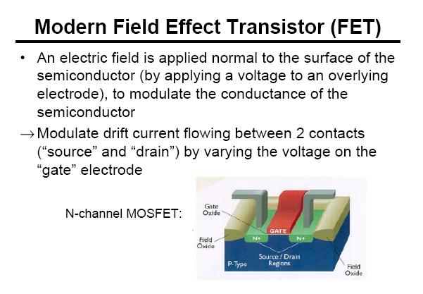
28 MOS Capacitors MOS: Metal-Oxide-Semiconductor V g metal gate V g gate SiO 2 N + SiO 2 N + Si body P-body MOS capacitor MOS transistor EE143 Ali Javey
29 Ideal MOS Capacitor Oxide has zero charge, and no current can pass through it. No charge centers are present in the oxide or at the oxidesemiconductor interface. Semiconductor is uniformly doped Φ M = Φ S = χ + (E C E F ) FB
30 Ideal MOS Capacitor At Equilibrium:
31 Ideal MOS Capacitor Under Bias Let us ground the semiconductor and start applying different voltages, V G, to the gate V G can be positive, negative or zero with respect to the semiconductor E F,metal E F,semiconductor = qv G Since oxide has no charge (it s an insulator with no available carriers or dopants), d E oxide / dx = ρ/ε = 0; meaning that the E-field inside the oxide is constant.
32 Inversion condition If we continue to increase the positive gate voltage, the bands at the semiconductor bends more strongly. At sufficiently high voltage, E i can be below E F indicating large concentration of electrons in the conduction band. We say the material near the surface is inverted. The inverted layer is not gotten by chemical doping, but by applying E-field. Where did we get the electrons from? When E i (surface) E i (bulk) = 2 [E F E i (bulk)], the condition is start of inversion, and the voltage V G applied to gate is called V T (threshold voltage). For V G > V T, the Si surface is inverted.
33
34 Ideal MOS Capacitor n-type Si
35
36 Electrostatic potential, φ(x) Define a new term, φ(x) taken to be the potential inside the semiconductor at a given point x. [The symbol φ instead of V used in MOS work to avoid confusion with externally applied voltage, V] 1 φ( x) = [ Ei (bulk) Ei q ( x)] Potential at any point x φ S = 1 q [ E i (bulk) E i (surface)] Surface potential φ F = 1 q [ E i (bulk) E F ] φ F related to doping concentration φ F > 0 means p-type φ F < 0 means n-type
37 Electrostatic potential φ S is positive if the bands bend\.? φ S = 2φ F at the depletion-inversion transition point (threshold voltage)
38 Charge Density - Accumulation p-type silicon accumulation condition V G < 0 M O S p-si The accumulation charges in the semiconductor are., and appear close to the surface and fall-off rapidly as x increases. One can assume that the free carrier concentration at the oxide-semiconductor interface is a δ-function. Accumulation of holes x Charge on metal = Q M Charge on semiconductor = (charge on metal) Q Accumulation = Q M
39 Charge Density - Depletion p-type Si, depletion condition The depletion charges in Si are immobile ions - results in depletion layer similar to that in pn junction or Schottky diode. V G > 0 M O S p-si q N A A W = Q M ( ) (+) If surface potential is φ s, then the depletion layer width W will be Q M w Depletion of holes W = 2ε qn Si A φ S Does this equation look familiar?
40 Charge Density - Inversion p-type Si, strong inversion Once inversion charges appear, they remain close to the surface since they are.. Any additional voltage to the gate results in extra Q M in gate and get compensated by extra inversion electrons in semiconductor. V G >>0 Q M M O S w p-si Depletion of holes Inversion electrons: δ-function-like So, the depletion width does not change during inversion. Electrons appear as δ- function near the surface. Maximum depletion layer width W = W T
41 MOS C-V characteristics The measured MOS capacitance (called gate capacitance) varies with the applied gate voltage A very powerful diagnostic tool for identifying threshold voltage, oxide thickness, substrate doping concentration, and flat band voltage. It also tells you how close to an ideal MOSC your structure is. Measurement of C-V characteristics Apply any dc bias, and superimpose a small (15 mv) ac signal (typically 1 khz 1 MHz)
42 C-V: under accumulation Consider p-type Si under accumulation. V G < 0 M O S p-si V G < 0. Looks similar to parallel plate capacitor. Accumulation of holes C G = C ox where C ox = (ε ox A) / x ox x C G is constant as a function of V G
43 C-V: under depletion Depletion condition: V G > 0 V G > 0 M O S p-type Si C G is C ox in series with C s where C s can be defined as semiconductor capacitance Q M C ox W C s Depletion of holes C ox = ε ox A / x ox C s = ε Si A / W C G = C ox C s / (C ox + C S ) 2ε W = qn Si A φ where φ s is surface potential s C G decreases with increasing V G
44 C-V: under inversion (high frequency) V G = V T and V G > V T Inversion condition φ s = 2 φ F W = W 2ε Si T = 2 q NA At high frequency, inversion electrons are not able to respond to ac voltage. C ox = ε ox A / x ox φ C s = ε Si A / W T C G (ω )= C ox C s / (C ox + C S ) F V G >>0 Q M M O S W p-si Inversion electrons δ- function Depletion of holes C ox C s C G will be constant for V G V T
45 C-V: under inversion (low frequency) At low frequency, the inversion electrons will be able to respond to the ac voltage. So, the gate capacitance will be equal to the oxide capacitance (similar to a parallel plate capacitance). C G (ω 0) = C ox = ε ox A / x ox C ox C low frequency high frequency V fb V t accumulation depletion inversion V g Ideal MOSC (p-type Si) C G increases for V G V T until it reaches C ox
46 The First Transistor

47 1956 Physics Nobel Prize
48 Invention of the Field-Effect Transistor In 1935, a British patent was issued to Oskar Heil. A working MOSFET was not demonstrated until 1955.
49

50 Today s MOSFET Technology Gate oxides as thin as 1.2 nm can be manufactured reproducibly. Large tunneling current through the oxide limits oxide-thickness reduction.

51 Introduction to the MOSFET Basic MOSFET structure and IV characteristics
52 Introduction to the MOSFET Two ways of representing a MOSFET:
53
54 Complementary MOSFETs (CMOS) NFET PFET When V g = V dd, the NFET is on and the PFET is off. When V g = 0, the PFET is on and the NFET is off.
55 Qualitative discussion: n-mosfet V G > V T ; V DS 0 I D increases with V DS V G > V T ; V DS small, > 0 I D increases with V DS, but rate of increase decreases. V G > V T ; V DS pinch-off I D reaches a saturation value, I D,sat The V DS value is called V DS,sat V G > V T ; V DS > V DS,sat I D does not increase further, saturation region.
56 Threshold voltage for NMOS and PMOS When V G = V T, φ s = 2 φ F ; we get expression for V T. V ε 2q N 2 φ Si A T = φf + xox 2 εox εsi F Ideal n-channel (p-silicon) device both terms positive V T ε 2 = 2φ + Si q ND F xox 2φF εox εsi ε Si / ε ox = = 11.9 / Ideal p-channel (n-silicon) device both terms negative 1 φf = [ Ei (bulk) EF] q φ F > 0 means p-type φ F < 0 means n-type
57 How to Measure the V T of a MOSFET I ds V ds = 10mV V t V t is measured by extrapolating the I ds versus V gs (at low V ds ) curve to I ds = 0. V gs I dsat W = Coxe( Vgs Vt ) μnsv L ds V gs V t
58 Quantitative I D -V DS Relationships 1 st attempt I D = Zμ L n C ox ( V V ) G T Square Law V DS 2 DS V 2 < V DS < ; DS, sat V G > VT 0 V I D will increase as V DS is increased, but when V G V DS = V T, pinch-off occurs, and current saturates when V DS is increased further. This value of V DS is called V DS,sat. i.e., V DS,sat = V G V T and the current when V DS = V DS,sat is called I DS,sat. I D,sat Z μc 2 L = ox G T D V DS, sat ( V V ) 2 V > ; V G > VT Here, C ox is the oxide capacitance per unit area, C ox = ε ox / x ox
59 I D -V DS characteristics expected from a long channel (ΔL << L) MOSFET (n-channel), for various values of V G
60 N-channel MOSFET Layout (Top View) 4 lithography steps are required: 1. active area 2. gate electrode 3. contacts 4. metal interconnects EE143 Ali Javey
61 Simple NMOS Process Flow 1) Thermal oxidation (~10 nm pad oxide ) 2) Silicon-nitride (Si 3 N 4 ) deposition by CVD (~40nm) 3) Active-area definition (lithography & etch) 4) Boron ion implantation ( channel stop implant) EE143 Ali Javey
62 5) Thermal oxidation to grow oxide in field regions 6) Si 3 N 4 & pad oxide removal 7) Thermal oxidation ( gate oxide ) 8) Poly-Si deposition by CVD 9) Poly-Si gate-electrode patterning (litho. & etch) Simple NMOS Process Flow 10) P or As ion implantation to form n+ source and drain regions Top view of masks EE143 Ali Javey
63 Simple NMOS Process Flow 11) SiO 2 CVD Top view of masks 12) Contact definition (litho. & etch) 13) Al deposition by sputtering 14) Al patterning by litho. & etch to form interconnects EE143 Ali Javey
Extensive reading materials on reserve, including
 Section 12: Intro to Devices Extensive reading materials on reserve, including Robert F. Pierret, Semiconductor Device Fundamentals EE143 Ali Javey Bond Model of Electrons and Holes Si Si Si Si Si Si Si
Section 12: Intro to Devices
 Section 12: Intro to Devices Extensive reading materials on reserve, including Robert F. Pierret, Semiconductor Device Fundamentals Bond Model of Electrons and Holes Si Si Si Si Si Si Si Si Si Silicon
EECS130 Integrated Circuit Devices
 EECS130 Integrated Circuit Devices Professor Ali Javey 10/02/2007 MS Junctions, Lecture 2 MOS Cap, Lecture 1 Reading: finish chapter14, start chapter16 Announcements Professor Javey will hold his OH at
Lecture 04 Review of MOSFET
 ECE 541/ME 541 Microelectronic Fabrication Techniques Lecture 04 Review of MOSFET Zheng Yang (ERF 3017, email: yangzhen@uic.edu) What is a Transistor? A Switch! An MOS Transistor V GS V T V GS S Ron D
EE105 - Fall 2006 Microelectronic Devices and Circuits
 EE105 - Fall 2006 Microelectronic Devices and Circuits Prof. Jan M. Rabaey (jan@eecs) Lecture 7: MOS Transistor Some Administrative Issues Lab 2 this week Hw 2 due on We Hw 3 will be posted same day MIDTERM
EE105 - Fall 2005 Microelectronic Devices and Circuits
 EE105 - Fall 005 Microelectronic Devices and Circuits ecture 7 MOS Transistor Announcements Homework 3, due today Homework 4 due next week ab this week Reading: Chapter 4 1 ecture Material ast lecture
Fundamentals of the Metal Oxide Semiconductor Field-Effect Transistor
 Triode Working FET Fundamentals of the Metal Oxide Semiconductor Field-Effect Transistor The characteristics of energy bands as a function of applied voltage. Surface inversion. The expression for the
Semiconductor Physics Problems 2015
 Semiconductor Physics Problems 2015 Page and figure numbers refer to Semiconductor Devices Physics and Technology, 3rd edition, by SM Sze and M-K Lee 1. The purest semiconductor crystals it is possible
Lecture 12: MOS Capacitors, transistors. Context
 Lecture 12: MOS Capacitors, transistors Context In the last lecture, we discussed PN diodes, and the depletion layer into semiconductor surfaces. Small signal models In this lecture, we will apply those
MOS CAPACITOR AND MOSFET
 EE336 Semiconductor Devices 1 MOS CAPACITOR AND MOSFET Dr. Mohammed M. Farag Ideal MOS Capacitor Semiconductor Devices Physics and Technology Chapter 5 EE336 Semiconductor Devices 2 MOS Capacitor Structure
ESE 570: Digital Integrated Circuits and VLSI Fundamentals
 ESE 570: Digital Integrated Circuits and VLSI Fundamentals Lec 4: January 23, 2018 MOS Transistor Theory, MOS Model Penn ESE 570 Spring 2018 Khanna Lecture Outline! CMOS Process Enhancements! Semiconductor
Classification of Solids
 Classification of Solids Classification by conductivity, which is related to the band structure: (Filled bands are shown dark; D(E) = Density of states) Class Electron Density Density of States D(E) Examples
Lecture 12: MOSFET Devices
 Lecture 12: MOSFET Devices Gu-Yeon Wei Division of Engineering and Applied Sciences Harvard University guyeon@eecs.harvard.edu Wei 1 Overview Reading S&S: Chapter 5.1~5.4 Supplemental Reading Background
Lecture 11: MOS Transistor
 Lecture 11: MOS Transistor Prof. Niknejad Lecture Outline Review: MOS Capacitors Regions MOS Capacitors (3.8 3.9) CV Curve Threshold Voltage MOS Transistors (4.1 4.3): Overview Cross-section and layout
ESE 570: Digital Integrated Circuits and VLSI Fundamentals
 ESE 570: Digital Integrated Circuits and VLSI Fundamentals Lec 4: January 29, 2019 MOS Transistor Theory, MOS Model Penn ESE 570 Spring 2019 Khanna Lecture Outline! CMOS Process Enhancements! Semiconductor
ESE 570: Digital Integrated Circuits and VLSI Fundamentals
 ESE 570: Digital Integrated Circuits and VLSI Fundamentals Lec 4: January 24, 2017 MOS Transistor Theory, MOS Model Penn ESE 570 Spring 2017 Khanna Lecture Outline! Semiconductor Physics " Band gaps "
Electrical Resistance
 Electrical Resistance I + V _ W Material with resistivity ρ t L Resistance R V I = L ρ Wt (Unit: ohms) where ρ is the electrical resistivity 1 Adding parts/billion to parts/thousand of dopants to pure
UNIVERSITY OF CALIFORNIA College of Engineering Department of Electrical Engineering and Computer Sciences. EECS 130 Professor Ali Javey Fall 2006
 UNIVERSITY OF CALIFORNIA College of Engineering Department of Electrical Engineering and Computer Sciences EECS 130 Professor Ali Javey Fall 2006 Midterm 2 Name: SID: Closed book. Two sheets of notes are
Semiconductor Physics fall 2012 problems
 Semiconductor Physics fall 2012 problems 1. An n-type sample of silicon has a uniform density N D = 10 16 atoms cm -3 of arsenic, and a p-type silicon sample has N A = 10 15 atoms cm -3 of boron. For each
FIELD-EFFECT TRANSISTORS
 FIEL-EFFECT TRANSISTORS 1 Semiconductor review 2 The MOS capacitor 2 The enhancement-type N-MOS transistor 3 I-V characteristics of enhancement MOSFETS 4 The output characteristic of the MOSFET in saturation
MOS Transistor I-V Characteristics and Parasitics
 ECEN454 Digital Integrated Circuit Design MOS Transistor I-V Characteristics and Parasitics ECEN 454 Facts about Transistors So far, we have treated transistors as ideal switches An ON transistor passes
CMPEN 411 VLSI Digital Circuits. Lecture 03: MOS Transistor
 CMPEN 411 VLSI Digital Circuits Lecture 03: MOS Transistor Kyusun Choi [Adapted from Rabaey s Digital Integrated Circuits, Second Edition, 2003 J. Rabaey, A. Chandrakasan, B. Nikolic] CMPEN 411 L03 S.1
The Devices. Digital Integrated Circuits A Design Perspective. Jan M. Rabaey Anantha Chandrakasan Borivoje Nikolic. July 30, 2002
 igital Integrated Circuits A esign Perspective Jan M. Rabaey Anantha Chandrakasan Borivoje Nikolic The evices July 30, 2002 Goal of this chapter Present intuitive understanding of device operation Introduction
ECE 340 Lecture 39 : MOS Capacitor II
 ECE 340 Lecture 39 : MOS Capacitor II Class Outline: Effects of Real Surfaces Threshold Voltage MOS Capacitance-Voltage Analysis Things you should know when you leave Key Questions What are the effects
Electrical Characteristics of MOS Devices
 Electrical Characteristics of MOS Devices The MOS Capacitor Voltage components Accumulation, Depletion, Inversion Modes Effect of channel bias and substrate bias Effect of gate oide charges Threshold-voltage
Lecture 15 OUTLINE. MOSFET structure & operation (qualitative) Review of electrostatics The (N)MOS capacitor
 Review of electrostatics The (N)MOS capacitor") Lecture 15 OUTLINE MOSFET structure & operation (qualitative) Review of electrostatics The (N)MOS capacitor Electrostatics Charge vs. voltage characteristic Reading: Chapter 6.1 6.2.1 EE15 Spring 28 Lecture
Lecture 15 OUTLINE MOSFET structure & operation (qualitative) Review of electrostatics The (N)MOS capacitor Electrostatics Charge vs. voltage characteristic Reading: Chapter 6.1 6.2.1 EE15 Spring 28 Lecture
! CMOS Process Enhancements. ! Semiconductor Physics. " Band gaps. " Field Effects. ! MOS Physics. " Cut-off. " Depletion.
 ESE 570: Digital Integrated Circuits and VLSI Fundamentals Lec 4: January 3, 018 MOS Transistor Theory, MOS Model Lecture Outline! CMOS Process Enhancements! Semiconductor Physics " Band gaps " Field Effects!
MOSFET: Introduction
 E&CE 437 Integrated VLSI Systems MOS Transistor 1 of 30 MOSFET: Introduction Metal oxide semiconductor field effect transistor (MOSFET) or MOS is widely used for implementing digital designs Its major
! CMOS Process Enhancements. ! Semiconductor Physics. " Band gaps. " Field Effects. ! MOS Physics. " Cut-off. " Depletion.
 ESE 570: Digital Integrated Circuits and VLSI Fundamentals Lec 4: January 9, 019 MOS Transistor Theory, MOS Model Lecture Outline CMOS Process Enhancements Semiconductor Physics Band gaps Field Effects
Device Models (PN Diode, MOSFET )
") Device Models (PN Diode, MOSFET ) Instructor: Steven P. Levitan steve@ece.pitt.edu TA: Gayatri Mehta, José Martínez Book: Digital Integrated Circuits: A Design Perspective; Jan Rabaey Lab Notes: Handed
Device Models (PN Diode, MOSFET ) Instructor: Steven P. Levitan steve@ece.pitt.edu TA: Gayatri Mehta, José Martínez Book: Digital Integrated Circuits: A Design Perspective; Jan Rabaey Lab Notes: Handed
Final Examination EE 130 December 16, 1997 Time allotted: 180 minutes
 Final Examination EE 130 December 16, 1997 Time allotted: 180 minutes Problem 1: Semiconductor Fundamentals [30 points] A uniformly doped silicon sample of length 100µm and cross-sectional area 100µm 2
Lecture 15 OUTLINE. MOSFET structure & operation (qualitative) Review of electrostatics The (N)MOS capacitor
 Review of electrostatics The (N)MOS capacitor") Lecture 15 OUTLINE MOSFET structure & operation (qualitative) Review of electrostatics The (N)MOS capacitor Electrostatics t ti Charge vs. voltage characteristic Reading: Chapter 6.1 6.2.1 EE105 Fall 2007
Lecture 15 OUTLINE MOSFET structure & operation (qualitative) Review of electrostatics The (N)MOS capacitor Electrostatics t ti Charge vs. voltage characteristic Reading: Chapter 6.1 6.2.1 EE105 Fall 2007
The Devices. Digital Integrated Circuits A Design Perspective. Jan M. Rabaey Anantha Chandrakasan Borivoje Nikolic. July 30, 2002
 Digital Integrated Circuits A Design Perspective Jan M. Rabaey Anantha Chandrakasan Borivoje Nikolic The Devices July 30, 2002 Goal of this chapter Present intuitive understanding of device operation Introduction
P. R. Nelson 1 ECE418 - VLSI. Midterm Exam. Solutions
 P. R. Nelson 1 ECE418 - VLSI Midterm Exam Solutions 1. (8 points) Draw the cross-section view for A-A. The cross-section view is as shown below.. ( points) Can you tell which of the metal1 regions is the
EECS130 Integrated Circuit Devices
 EECS130 Integrated Circuit Devices Professor Ali Javey 8/30/2007 Semiconductor Fundamentals Lecture 2 Read: Chapters 1 and 2 Last Lecture: Energy Band Diagram Conduction band E c E g Band gap E v Valence
an introduction to Semiconductor Devices
 an introduction to Semiconductor Devices Donald A. Neamen Chapter 6 Fundamentals of the Metal-Oxide-Semiconductor Field-Effect Transistor Introduction: Chapter 6 1. MOSFET Structure 2. MOS Capacitor -
MOS Transistors. Prof. Krishna Saraswat. Department of Electrical Engineering Stanford University Stanford, CA
 MOS Transistors Prof. Krishna Saraswat Department of Electrical Engineering S Stanford, CA 94305 saraswat@stanford.edu 1 1930: Patent on the Field-Effect Transistor! Julius Lilienfeld filed a patent describing
Device Models (PN Diode, MOSFET )
") Device Models (PN Diode, MOSFET ) Instructor: Steven P. Levitan steve@ece.pitt.edu TA: Gayatri Mehta, José Martínez Book: Digital Integrated Circuits: A Design Perspective; Jan Rabaey Lab Notes: Handed
Device Models (PN Diode, MOSFET ) Instructor: Steven P. Levitan steve@ece.pitt.edu TA: Gayatri Mehta, José Martínez Book: Digital Integrated Circuits: A Design Perspective; Jan Rabaey Lab Notes: Handed
Digital Integrated Circuits A Design Perspective. Jan M. Rabaey Anantha Chandrakasan Borivoje Nikolic. The Devices. July 30, Devices.
 Digital Integrated Circuits A Design Perspective Jan M. Rabaey Anantha Chandrakasan Borivoje Nikolic The July 30, 2002 1 Goal of this chapter Present intuitive understanding of device operation Introduction
The Devices: MOS Transistors
 The Devices: MOS Transistors References: Semiconductor Device Fundamentals, R. F. Pierret, Addison-Wesley Digital Integrated Circuits: A Design Perspective, J. Rabaey et.al. Prentice Hall NMOS Transistor
Lecture 6 PN Junction and MOS Electrostatics(III) Metal-Oxide-Semiconductor Structure
 Metal-Oxide-Semiconductor Structure") Lecture 6 PN Junction and MOS Electrostatics(III) Metal-Oxide-Semiconductor Structure Outline 1. Introduction to MOS structure 2. Electrostatics of MOS in thermal equilibrium 3. Electrostatics of MOS with
Lecture 6 PN Junction and MOS Electrostatics(III) Metal-Oxide-Semiconductor Structure Outline 1. Introduction to MOS structure 2. Electrostatics of MOS in thermal equilibrium 3. Electrostatics of MOS with
Lecture Outline. ESE 570: Digital Integrated Circuits and VLSI Fundamentals. Review: MOSFET N-Type, P-Type. Semiconductor Physics.
 ESE 57: Digital Integrated Circuits and VLSI Fundamentals Lec 4: January 24, 217 MOS Transistor Theory, MOS Model Lecture Outline! Semiconductor Physics " Band gaps " Field Effects! MOS Physics " Cutoff
Appendix 1: List of symbols
 Appendix 1: List of symbols Symbol Description MKS Units a Acceleration m/s 2 a 0 Bohr radius m A Area m 2 A* Richardson constant m/s A C Collector area m 2 A E Emitter area m 2 b Bimolecular recombination
SECTION: Circle one: Alam Lundstrom. ECE 305 Exam 5 SOLUTIONS: Spring 2016 April 18, 2016 M. A. Alam and M.S. Lundstrom Purdue University
 NAME: PUID: SECTION: Circle one: Alam Lundstrom ECE 305 Exam 5 SOLUTIONS: April 18, 2016 M A Alam and MS Lundstrom Purdue University This is a closed book exam You may use a calculator and the formula
n N D n p = n i p N A
 Summary of electron and hole concentration in semiconductors Intrinsic semiconductor: E G n kt i = pi = N e 2 0 Donor-doped semiconductor: n N D where N D is the concentration of donor impurity Acceptor-doped
1. The MOS Transistor. Electrical Conduction in Solids
 Electrical Conduction in Solids!The band diagram describes the energy levels for electron in solids.!the lower filled band is named Valence Band.!The upper vacant band is named conduction band.!the distance
EECS130 Integrated Circuit Devices
 EECS130 Integrated Circuit Devices Professor Ali Javey 9/18/2007 P Junctions Lecture 1 Reading: Chapter 5 Announcements For THIS WEEK OLY, Prof. Javey's office hours will be held on Tuesday, Sept 18 3:30-4:30
ECE 342 Electronic Circuits. Lecture 6 MOS Transistors
 ECE 342 Electronic Circuits Lecture 6 MOS Transistors Jose E. Schutt-Aine Electrical & Computer Engineering University of Illinois jesa@illinois.edu 1 NMOS Transistor Typically L = 0.1 to 3 m, W = 0.2
1 Name: Student number: DEPARTMENT OF PHYSICS AND PHYSICAL OCEANOGRAPHY MEMORIAL UNIVERSITY OF NEWFOUNDLAND. Fall :00-11:00
 1 Name: DEPARTMENT OF PHYSICS AND PHYSICAL OCEANOGRAPHY MEMORIAL UNIVERSITY OF NEWFOUNDLAND Final Exam Physics 3000 December 11, 2012 Fall 2012 9:00-11:00 INSTRUCTIONS: 1. Answer all seven (7) questions.
ECE 342 Electronic Circuits. 3. MOS Transistors
 ECE 342 Electronic Circuits 3. MOS Transistors Jose E. Schutt-Aine Electrical & Computer Engineering University of Illinois jschutt@emlab.uiuc.edu 1 NMOS Transistor Typically L = 0.1 to 3 m, W = 0.2 to
Semiconductor Physics fall 2012 problems
 Semiconductor Physics fall 2012 problems 1. An n-type sample of silicon has a uniform density N D = 10 16 atoms cm -3 of arsenic, and a p-type silicon sample has N A = 10 15 atoms cm -3 of boron. For each
Lecture 2. Introduction to semiconductors Structures and characteristics in semiconductors
 Lecture 2 Introduction to semiconductors Structures and characteristics in semiconductors Semiconductor p-n junction Metal Oxide Silicon structure Semiconductor contact Literature Glen F. Knoll, Radiation
Midterm I - Solutions
 UNIVERSITY OF CALIFORNIA College of Engineering Department of Electrical Engineering and Computer Sciences EECS 130 Spring 2008 Professor Chenming Hu Midterm I - Solutions Name: SID: Grad/Undergrad: Closed
Chapter 1 Overview of Semiconductor Materials and Physics
 Chapter 1 Overview of Semiconductor Materials and Physics Professor Paul K. Chu Conductivity / Resistivity of Insulators, Semiconductors, and Conductors Semiconductor Elements Period II III IV V VI 2 B
Chapter 7. The pn Junction
 Chapter 7 The pn Junction Chapter 7 PN Junction PN junction can be fabricated by implanting or diffusing donors into a P-type substrate such that a layer of semiconductor is converted into N type. Converting
Integrated Circuits & Systems
 Federal University of Santa Catarina Center for Technology Computer Science & Electronics Engineering Integrated Circuits & Systems INE 5442 Lecture 10 MOSFET part 1 guntzel@inf.ufsc.br ual-well Trench-Isolated
Lecture 3: CMOS Transistor Theory
 Lecture 3: CMOS Transistor Theory Outline Introduction MOS Capacitor nmos I-V Characteristics pmos I-V Characteristics Gate and Diffusion Capacitance 2 Introduction So far, we have treated transistors
MOS Transistor Properties Review
 MOS Transistor Properties Review 1 VLSI Chip Manufacturing Process Photolithography: transfer of mask patterns to the chip Diffusion or ion implantation: selective doping of Si substrate Oxidation: SiO
Session 6: Solid State Physics. Diode
 Session 6: Solid State Physics Diode 1 Outline A B C D E F G H I J 2 Definitions / Assumptions Homojunction: the junction is between two regions of the same material Heterojunction: the junction is between
Class 05: Device Physics II
 Topics: 1. Introduction 2. NFET Model and Cross Section with Parasitics 3. NFET as a Capacitor 4. Capacitance vs. Voltage Curves 5. NFET as a Capacitor - Band Diagrams at V=0 6. NFET as a Capacitor - Accumulation
EE 560 MOS TRANSISTOR THEORY
 1 EE 560 MOS TRANSISTOR THEORY PART 1 TWO TERMINAL MOS STRUCTURE V G (GATE VOLTAGE) 2 GATE OXIDE SiO 2 SUBSTRATE p-type doped Si (N A = 10 15 to 10 16 cm -3 ) t ox V B (SUBSTRATE VOLTAGE) EQUILIBRIUM:
Lecture 4: CMOS Transistor Theory
 Introduction to CMOS VLSI Design Lecture 4: CMOS Transistor Theory David Harris, Harvey Mudd College Kartik Mohanram and Steven Levitan University of Pittsburgh Outline q Introduction q MOS Capacitor q
Charge Carriers in Semiconductor
 Charge Carriers in Semiconductor To understand PN junction s IV characteristics, it is important to understand charge carriers behavior in solids, how to modify carrier densities, and different mechanisms
Quiz #1 Practice Problem Set
 Name: Student Number: ELEC 3908 Physical Electronics Quiz #1 Practice Problem Set? Minutes January 22, 2016 - No aids except a non-programmable calculator - All questions must be answered - All questions
Lecture 2. Introduction to semiconductors Structures and characteristics in semiconductors
 Lecture 2 Introduction to semiconductors Structures and characteristics in semiconductors Semiconductor p-n junction Metal Oxide Silicon structure Semiconductor contact Literature Glen F. Knoll, Radiation
ESE370: Circuit-Level Modeling, Design, and Optimization for Digital Systems
 ESE370: Circuit-Level Modeling, Design, and Optimization for Digital Systems Lec 6: September 14, 2015 MOS Model You are Here: Transistor Edition! Previously: simple models (0 and 1 st order) " Comfortable
Part 4: Heterojunctions - MOS Devices. MOSFET Current Voltage Characteristics
 MOS Device Uses: Part 4: Heterojunctions - MOS Devices MOSCAP capacitor: storing charge, charge-coupled device (CCD), etc. MOSFET transistor: switch, current amplifier, dynamic random access memory (DRAM-volatile),
EECS143 Microfabrication Technology
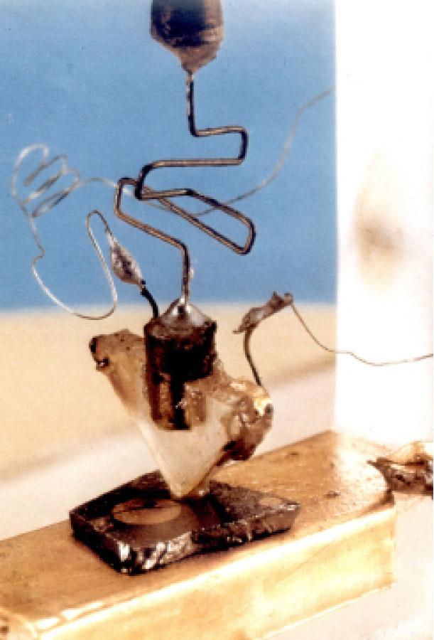
 EECS143 Microfabrication Technology Professor Ali Javey Introduction to Materials Lecture 1 Evolution of Devices Yesterday s Transistor (1947) Today s Transistor (2006) Why Semiconductors? Conductors e.g
ESE370: Circuit-Level Modeling, Design, and Optimization for Digital Systems
 ESE370: Circuit-Level Modeling, Design, and Optimization for Digital Systems Lec 6: September 18, 2017 MOS Model You are Here: Transistor Edition! Previously: simple models (0 and 1 st order) " Comfortable
Semiconductor Devices. C. Hu: Modern Semiconductor Devices for Integrated Circuits Chapter 5
 Semiconductor Devices C. Hu: Modern Semiconductor Devices for Integrated Circuits Chapter 5 Global leader in environmental and industrial measurement Wednesday 3.2. afternoon Tour around facilities & lecture
Student Number: CARLETON UNIVERSITY SELECTED FINAL EXAMINATION QUESTIONS
 Name: CARLETON UNIVERSITY SELECTE FINAL EXAMINATION QUESTIONS URATION: 6 HOURS epartment Name & Course Number: ELEC 3908 Course Instructors: S. P. McGarry Authorized Memoranda: Non-programmable calculators
EE105 Fall 2015 Microelectronic Devices and Circuits: Semiconductor Fabrication and PN Junctions
 EE105 Fall 2015 Microelectronic Devices and Circuits: Semiconductor Fabrication and PN Junctions Prof. Ming C. Wu wu@eecs.berkeley.edu 511 Sutardja Dai Hall (SDH) 1 pn Junction p-type semiconductor in
MOS Capacitor MOSFET Devices. MOSFET s. INEL Solid State Electronics. Manuel Toledo Quiñones. ECE Dept. UPRM.
 INEL 6055 - Solid State Electronics ECE Dept. UPRM 20th March 2006 Definitions MOS Capacitor Isolated Metal, SiO 2, Si Threshold Voltage qφ m metal d vacuum level SiO qχ 2 E g /2 qφ F E C E i E F E v qφ
Semiconductor Junctions
 8 Semiconductor Junctions Almost all solar cells contain junctions between different materials of different doping. Since these junctions are crucial to the operation of the solar cell, we will discuss
ECE 305 Exam 5 SOLUTIONS: Spring 2015 April 17, 2015 Mark Lundstrom Purdue University
 NAME: PUID: : ECE 305 Exam 5 SOLUTIONS: April 17, 2015 Mark Lundstrom Purdue University This is a closed book exam. You may use a calculator and the formula sheet at the end of this exam. Following the
MOS Transistor Theory MOSFET Symbols Current Characteristics of MOSFET. MOS Symbols and Characteristics. nmos Enhancement Transistor
 MOS Transistor Theory MOSFET Symbols Current Characteristics of MOSFET Calculation of t and Important 2 nd Order Effects SmallSignal Signal MOSFET Model Summary Material from: CMOS LSI Design By Weste
Lecture 5: CMOS Transistor Theory
 Lecture 5: CMOS Transistor Theory Slides courtesy of Deming Chen Slides based on the initial set from David Harris CMOS VLSI Design Outline q q q q q q q Introduction MOS Capacitor nmos I-V Characteristics
Lecture #27. The Short Channel Effect (SCE)
") Lecture #27 ANNOUNCEMENTS Design Project: Your BJT design should meet the performance specifications to within 10% at both 300K and 360K. ( β dc > 45, f T > 18 GHz, V A > 9 V and V punchthrough > 9 V )
Lecture #27 ANNOUNCEMENTS Design Project: Your BJT design should meet the performance specifications to within 10% at both 300K and 360K. ( β dc > 45, f T > 18 GHz, V A > 9 V and V punchthrough > 9 V )
Consider a uniformly doped PN junction, in which one region of the semiconductor is uniformly doped with acceptor atoms and the adjacent region is
 CHAPTER 7 The PN Junction Consider a uniformly doped PN junction, in which one region of the semiconductor is uniformly doped with acceptor atoms and the adjacent region is uniformly doped with donor atoms.
Semiconductor Device Physics
 1 Semiconductor Device Physics Lecture 3 http://zitompul.wordpress.com 2 0 1 3 Semiconductor Device Physics 2 Three primary types of carrier action occur inside a semiconductor: Drift: charged particle
Theory of Electrical Characterization of Semiconductors
 Theory of Electrical Characterization of Semiconductors P. Stallinga Universidade do Algarve U.C.E.H. A.D.E.E.C. OptoElectronics SELOA Summer School May 2000, Bologna (It) Overview Devices: bulk Schottky
Lecture 15: MOS Transistor models: Body effects, SPICE models. Context. In the last lecture, we discussed the modes of operation of a MOS FET:
 Lecture 15: MOS Transistor models: Body effects, SPICE models Context In the last lecture, we discussed the modes of operation of a MOS FET: oltage controlled resistor model I- curve (Square-Law Model)
ECE 497 JS Lecture - 12 Device Technologies
 ECE 497 JS Lecture - 12 Device Technologies Spring 2004 Jose E. Schutt-Aine Electrical & Computer Engineering University of Illinois jose@emlab.uiuc.edu 1 NMOS Transistor 2 ρ Source channel charge density
Content. MIS Capacitor. Accumulation Depletion Inversion MOS CAPACITOR. A Cantoni Digital Switching
 Content MIS Capacitor Accumulation Depletion Inversion MOS CAPACITOR 1 MIS Capacitor Metal Oxide C ox p-si C s Components of a capacitance model for the MIS structure 2 MIS Capacitor- Accumulation ρ( x)
CHAPTER 5 MOS FIELD-EFFECT TRANSISTORS
 CHAPTER 5 MOS FIELD-EFFECT TRANSISTORS 5.1 The MOS capacitor 5.2 The enhancement-type N-MOS transistor 5.3 I-V characteristics of enhancement mode MOSFETS 5.4 The PMOS transistor and CMOS technology 5.5
MOS Transistor Theory
 MOS Transistor Theory So far, we have viewed a MOS transistor as an ideal switch (digital operation) Reality: less than ideal EE 261 Krish Chakrabarty 1 Introduction So far, we have treated transistors
EECS130 Integrated Circuit Devices
 EECS130 Integrated Circuit Devices Professor Ali Javey 10/30/2007 MOSFETs Lecture 4 Reading: Chapter 17, 19 Announcements The next HW set is due on Thursday. Midterm 2 is next week!!!! Threshold and Subthreshold
Semiconductor Physics and Devices
 The pn Junction 1) Charge carriers crossing the junction. 3) Barrier potential Semiconductor Physics and Devices Chapter 8. The pn Junction Diode 2) Formation of positive and negative ions. 4) Formation
Course Administration. CPE/EE 427, CPE 527 VLSI Design I L04: MOS Transistors. Review: CMOS Process at a Glance
 Course Administration CPE/EE 7, CPE 7 VLI esign I L: MO Transistors epartment of Electrical and Computer Engineering University of Alabama in Huntsville Aleksandar Milenkovic ( www.ece.uah.edu/~milenka
UNIVERSITY OF CALIFORNIA College of Engineering Department of Electrical Engineering and Computer Sciences. Professor Chenming Hu.
 UNIVERSITY OF CALIFORNIA College of Engineering Department of Electrical Engineering and Computer Sciences EECS 130 Spring 2009 Professor Chenming Hu Midterm I Name: Closed book. One sheet of notes is
Review Energy Bands Carrier Density & Mobility Carrier Transport Generation and Recombination
 Review Energy Bands Carrier Density & Mobility Carrier Transport Generation and Recombination The Metal-Semiconductor Junction: Review Energy band diagram of the metal and the semiconductor before (a)
Junction Diodes. Tim Sumner, Imperial College, Rm: 1009, x /18/2006
 Junction Diodes Most elementary solid state junction electronic devices. They conduct in one direction (almost correct). Useful when one converts from AC to DC (rectifier). But today diodes have a wide
Chapter 4 Field-Effect Transistors
 Chapter 4 Field-Effect Transistors Microelectronic Circuit Design Richard C. Jaeger Travis N. Blalock 5/5/11 Chap 4-1 Chapter Goals Describe operation of MOSFETs. Define FET characteristics in operation
! Previously: simple models (0 and 1 st order) " Comfortable with basic functions and circuits. ! This week and next (4 lectures)
 Comfortable with basic functions and circuits. ! This week and next (4 lectures)") ESE370: CircuitLevel Modeling, Design, and Optimization for Digital Systems Lec 6: September 14, 2015 MOS Model You are Here: Transistor Edition! Previously: simple models (0 and 1 st order) " Comfortable
ESE370: CircuitLevel Modeling, Design, and Optimization for Digital Systems Lec 6: September 14, 2015 MOS Model You are Here: Transistor Edition! Previously: simple models (0 and 1 st order) " Comfortable
GaN based transistors
 GaN based transistors S FP FP dielectric G SiO 2 Al x Ga 1-x N barrier i-gan Buffer i-sic D Transistors "The Transistor was probably the most important invention of the 20th Century The American Institute
Diodes. anode. cathode. cut-off. Can be approximated by a piecewise-linear-like characteristic. Lecture 9-1
 Diodes mplest nonlinear circuit element Basic operation sets the foundation for Bipolar Junction Transistors (BJTs) Also present in Field Effect Transistors (FETs) Ideal diode characteristic anode cathode
MOS Capacitors ECE 2204
 MOS apacitors EE 2204 Some lasses of Field Effect Transistors Metal-Oxide-Semiconductor Field Effect Transistor MOSFET, which will be the type that we will study in this course. Metal-Semiconductor Field
PN Junction
 P Junction 2017-05-04 Definition Power Electronics = semiconductor switches are used Analogue amplifier = high power loss 250 200 u x 150 100 u Udc i 50 0 0 50 100 150 200 250 300 350 400 i,u dc i,u u
8.1 Drift diffusion model
 8.1 Drift diffusion model Advanced theory 1 Basic Semiconductor Equations The fundamentals of semiconductor physic are well described by tools of quantum mechanic. This point of view gives us a model of
Current mechanisms Exam January 27, 2012
 Current mechanisms Exam January 27, 2012 There are four mechanisms that typically cause currents to flow: thermionic emission, diffusion, drift, and tunneling. Explain briefly which kind of current mechanisms