EE241 - Spring 2001 Advanced Digital Integrated Circuits
|
|
|
- Darcy Hall
- 5 years ago
- Views:
Transcription
1 EE241 - Spring 21 Advanced Digital Integrated Circuits Lecture 12 Low Power Design Self-Resetting Logic Signals are pulses, not levels 1

2 Self-Resetting Logic Sense-Amplifying Logic Matsui, JSSC 12/94 2


3 SA-F/F Falling edge Rising edge Dynamic Logic with SA-F/F 3

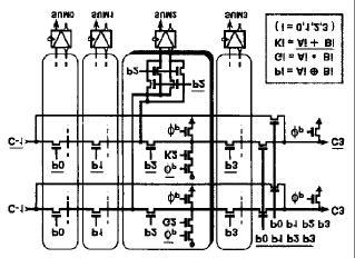
4 Example 4-Bit Adder 4


5 2-Bit Carry-Skip Adder GHz Logic with Sense Amplifiers Takahashi, JSSC 5/99 5


6 Read-out scheme Implemented Macros 6
")

7 Rotator (ROT) Incrementer (INC) 7
8 Low Power, Low Energy Circuit Design Architectures, Circuits and Technology Literature Chapter 4, Low-Voltage Technologies, by Kuroda and Sakurai Chapter 3, Techniques for Leakage Power Reduction, by De, et al. A. Chandrakasan and R. Brodersen, Low Power CMOS Design, Kluwer Academic Publishers, J. Rabaey and M. Pedram, Ed., Low Power Design Methodologies, Kluwer Academic Publishers, Proceedings of the IEEE, Special Issue on Low Power, April A. Chandrakasan and R. Brodersen, Low-Power CMOS Design, IEEE Press, 1998 (Reprint Volume) 8
9 Power vs. Energy Power in high performance systems» Peak power - power delivery, removal Energy in portable systems» Battery life Constant throughput vs. burst-mode computation Active vs. standby consumption Principles of Power Reduction P ~ α + ( C V + I t ) L swing ( I + I ) V DD DC Leak a - switching probability C L load capacitance V swing voltage swing f - frequency SC SC V DD I sc mean value of switching transient current t sc short current time I DC static current I leak leakage current f Dominant: P ~ α C L V swing V DD f Kuroda, Sakurai, IEICE 4/95 9
10 P ~ α C Active Power Reduction L V swing V DD Reducing switching probability (α)» Architectures» Power simulators/estimators (time consuming)» Glitching power reduction (15-2%) Reducing load capacitance» Technology scaling» Gate sizing, minimization, interconnect, CAD» Circuit techniques (PTL, ) Reducing supply voltage» Quadratic impact on power» Impact on delay how to maintain throughput? Reducing frequency f E ~ α C L V swing V DD Trends in Power Dissipation 1 x1.4 / 3 years 1 κ.7 Power Dissipation (W) x4 / 3 years 85 (a) Power dissipation vs. year. 9 Year MPU DSP 95 Power Density (mw/mm 2 ) 1 1 κ Scaling Factor κ inormalized by 4µm design rule j 1 (b) Power density vs. scaling factor. From Kuroda 1
11 Processor Power 1 Max Power (Watts) Pentium II (R) Pentium Pro (R) Pentium(R) 486 Pentium(R) MMX? m 1m.8m.6m.35m.25m.18m.13m Lead processor power increases every generation Compactions provide higher performance at lower power Power will be a problem Power (Watts) Pentium proc 18KW 5KW 1.5KW 5W Year Power delivery and dissipation will be prohibitive S. Borkar 11
12 Portability BATTERY (4+ lbs) Multimedia Terminals Laptop Computers Digital Cellular Telephony Nominal Capacity (Watt-hours / lb) Rechargable Lithium Nickel-Cadium Ni-Metal Hydride Year Expected Battery Lifetime increase over next 5 years: 3-4% Shannon Beats Moore s Law Algorithmic Complexity (Shannon s Law) 3G Processor Performance (~Moore s Law) 1 2G G Battery Capacity Source: Data compiled from multiple sources
13 Where Does Power Go in CMOS? Dynamic Power Consumption Charging and Discharging Capacitors Leakage Leaking transistors and diodes Short Circuit Currents Short Circuit Path between Supply Rails during Switching Dynamic Power Consumption V dd E ->1 = C L V dd 2 PMOS i supply A 1 NETWORK A N NMOS NETWORK V out C L E 1 T T Vdd = Pt ()dt = V i t dd supply ()dt = V C dv dd = C V L out L 2 dd T T Vdd 1 2 E = P t cap cap ()dt = V i t out cap ()dt = C V dv = -- C V L out out 2 L dd 13
14 Circuits with Reduced Swing V dd V dd V dd -V t C L E 1 = C L V dd ( V dd V t ) Can exploit reduced swing to lower power (e.g., reduced bit-line swing in memory) Dynamic Power Consumption - Revisited Power = Energy/transition * transition rate = C L * V dd 2 * f 1 = C L * V dd 2 * P 1 * f = C EFF * V dd 2 * f Power Dissipation is Data Dependent Function of Switching Activity C EFF = Effective Capacitance = C L * P 1 14
15 Node Transition Activity and Power Consider switching a CMOS gate for N clock cycles E N = C L V 2 dd nn ( ) E N : the energy consumed for N clock cycles n(n): the number of ->1 transition in N clock cycles P = lim avg N E N f N clk = nn ( ) lim C N N V fclk L dd α 1 = nn ( ) lim N N P avg = α 1 C L V 2 dd fclk Type of Logic Function: NOR vs. XOR 15
16 Type of Logic Function: NOR vs. XOR Transition Probabilities P ->1 (NOR,NAND) = (2 N -1)/2 2N P ->1 (XOR) = 1/4 16
17 Transition Probabilities for Basic Gates Transition Probability of 2-input NOR Gate 17
18 How about Dynamic Circuits? V DD φ M p Out In 1 In 2 In 3 PDN φ M e Power is Only Dissipated when Out=! C EFF = P(Out=).C L 2-input NAND Gate Example: Dynamic 2 Input NOR Gate Assume: P(A=1) = 1/2 P(B=1) = 1/2 Then: P(Out=) = 3/4 C EFF = 3/4 * C L Switching Activity Is Always Higher in Dynamic Circuits 18
19 Type of Logic Style: Static vs. Dynamic V dd V dd A CLK B A B C L A B C L CLK Power is only dissipated when Out=! STATIC NOR DYNAMIC NOR α ->1 = 3/16 N α 1 = N = Transition Probabilities for Dynamic Gates Switching Activity for Precharged Dynamic Gates P 1 = P 19
20 Another Logic Style: Dynamic DCVSL V dd V dd OUTB IN INB I OUT I Guaranteed transition for every operation! α ->1 = 1 Problem: Reconvergent Fanout A X B Z Reconvergence P(Z=1) = P(B=1). P(X=1 B=1) Becomes complex and intractable real fast 2
21 Glitching in Static CMOS also called: dynamic hazards A B X C Z ABC 11 X Z Unit Delay Observe: No glitching in dynamic circuits Example 1: Chain of NOR Gates 1 out1 out2 out3 out4 out V (Volt) out2 out8 out6 out4 out1 out3 out5 out t (nsec) 21
22 Example 2: Adder Circuit C in Add Add1 Add2 Add14 Add15 S S1 S2 S14 S15 Sum Output Voltage, Volts Cin S1 S Time, ns S15 How to Cope with Glitching? F 1 1 F 2 2 F 3 F 1 F F 3 Equalize Lengths of Timing Paths Through Design 22
23 Example: Carry Ripple versus Carry Lookahead A F A 1 A 2 A 3 A 4 A 5 A 6 A 7 Ripple A A 1 A 2 A 3 A 4 A 5 A 6 A 7 F Lookahead 23
EE241 - Spring 2000 Advanced Digital Integrated Circuits. Announcements
 EE241 - Spring 2 Advanced Digital Integrated Circuits Lecture 11 Low Power-Low Energy Circuit Design Announcements Homework #2 due Friday, 3/3 by 5pm Midterm project reports due in two weeks - 3/7 by 5pm
Lecture 8-1. Low Power Design
 Lecture 8 Konstantinos Masselos Department of Electrical & Electronic Engineering Imperial College London URL: http://cas.ee.ic.ac.uk/~kostas E-mail: k.masselos@ic.ac.uk Lecture 8-1 Based on slides/material
EE241 - Spring 2005 Advanced Digital Integrated Circuits. Admin. Lecture 10: Power Intro
 EE241 - Spring 2005 Advanced Digital Integrated Circuits Lecture 10: Power Intro Admin Project Phase 2 due Monday March 14, 5pm (by e-mail to jan@eecs.berkeley.edu and huifangq@eecs.berkeley.edu) Should
Power Dissipation. Where Does Power Go in CMOS?
 Power Dissipation [Adapted from Chapter 5 of Digital Integrated Circuits, 2003, J. Rabaey et al.] Where Does Power Go in CMOS? Dynamic Power Consumption Charging and Discharging Capacitors Short Circuit
EECS 427 Lecture 11: Power and Energy Reading: EECS 427 F09 Lecture Reminders
 EECS 47 Lecture 11: Power and Energy Reading: 5.55 [Adapted from Irwin and Narayanan] 1 Reminders CAD5 is due Wednesday 10/8 You can submit it by Thursday 10/9 at noon Lecture on 11/ will be taught by
Last Lecture. Power Dissipation CMOS Scaling. EECS 141 S02 Lecture 8
 EECS 141 S02 Lecture 8 Power Dissipation CMOS Scaling Last Lecture CMOS Inverter loading Switching Performance Evaluation Design optimization Inverter Sizing 1 Today CMOS Inverter power dissipation» Dynamic»
EE 466/586 VLSI Design. Partha Pande School of EECS Washington State University
 EE 466/586 VLSI Design Partha Pande School of EECS Washington State University pande@eecs.wsu.edu Lecture 8 Power Dissipation in CMOS Gates Power in CMOS gates Dynamic Power Capacitance switching Crowbar
Where Does Power Go in CMOS?
 Power Dissipation Where Does Power Go in CMOS? Dynamic Power Consumption Charging and Discharging Capacitors Short Circuit Currents Short Circuit Path between Supply Rails during Switching Leakage Leaking
CSE493/593. Designing for Low Power
 CSE493/593 Designing for Low Power Mary Jane Irwin [Adapted from Rabaey s Digital Integrated Circuits, 2002, J. Rabaey et al.].1 Why Power Matters Packaging costs Power supply rail design Chip and system
EE115C Winter 2017 Digital Electronic Circuits. Lecture 6: Power Consumption
 EE115C Winter 2017 Digital Electronic Circuits Lecture 6: Power Consumption Four Key Design Metrics for Digital ICs Cost of ICs Reliability Speed Power EE115C Winter 2017 2 Power and Energy Challenges
CMPEN 411 VLSI Digital Circuits Spring Lecture 14: Designing for Low Power
 CMPEN 411 VLSI Digital Circuits Spring 2012 Lecture 14: Designing for Low Power [Adapted from Rabaey s Digital Integrated Circuits, Second Edition, 2003 J. Rabaey, A. Chandrakasan, B. Nikolic] Sp12 CMPEN
EE141Microelettronica. CMOS Logic
 Microelettronica CMOS Logic CMOS logic Power consumption in CMOS logic gates Where Does Power Go in CMOS? Dynamic Power Consumption Charging and Discharging Capacitors Short Circuit Currents Short Circuit
THE INVERTER. Inverter
 THE INVERTER DIGITAL GATES Fundamental Parameters Functionality Reliability, Robustness Area Performance» Speed (delay)» Power Consumption» Energy Noise in Digital Integrated Circuits v(t) V DD i(t) (a)
Objective and Outline. Acknowledgement. Objective: Power Components. Outline: 1) Acknowledgements. Section 4: Power Components
 Acknowledgements. Section 4: Power Components") Objective: Power Components Outline: 1) Acknowledgements 2) Objective and Outline 1 Acknowledgement This lecture note has been obtained from similar courses all over the world. I wish to thank all the
Objective: Power Components Outline: 1) Acknowledgements 2) Objective and Outline 1 Acknowledgement This lecture note has been obtained from similar courses all over the world. I wish to thank all the
Announcements. EE141- Fall 2002 Lecture 7. MOS Capacitances Inverter Delay Power
 - Fall 2002 Lecture 7 MOS Capacitances Inverter Delay Power Announcements Wednesday 12-3pm lab cancelled Lab 4 this week Homework 2 due today at 5pm Homework 3 posted tonight Today s lecture MOS capacitances
Design for Manufacturability and Power Estimation. Physical issues verification (DSM)
") Design for Manufacturability and Power Estimation Lecture 25 Alessandra Nardi Thanks to Prof. Jan Rabaey and Prof. K. Keutzer Physical issues verification (DSM) Interconnects Signal Integrity P/G integrity
Design for Manufacturability and Power Estimation Lecture 25 Alessandra Nardi Thanks to Prof. Jan Rabaey and Prof. K. Keutzer Physical issues verification (DSM) Interconnects Signal Integrity P/G integrity
Announcements. EE141- Spring 2003 Lecture 8. Power Inverter Chain
 - Spring 2003 Lecture 8 Power Inverter Chain Announcements Homework 3 due today. Homework 4 will be posted later today. Special office hours from :30-3pm at BWRC (in lieu of Tuesday) Today s lecture Power
Topic 4. The CMOS Inverter
 Topic 4 The CMOS Inverter Peter Cheung Department of Electrical & Electronic Engineering Imperial College London URL: www.ee.ic.ac.uk/pcheung/ E-mail: p.cheung@ic.ac.uk Topic 4-1 Noise in Digital Integrated
L16: Power Dissipation in Digital Systems. L16: Spring 2007 Introductory Digital Systems Laboratory
 L16: Power Dissipation in Digital Systems 1 Problem #1: Power Dissipation/Heat Power (Watts) 100000 10000 1000 100 10 1 0.1 4004 80088080 8085 808686 386 486 Pentium proc 18KW 5KW 1.5KW 500W 1971 1974
MODULE III PHYSICAL DESIGN ISSUES
 VLSI Digital Design MODULE III PHYSICAL DESIGN ISSUES 3.2 Power-supply and clock distribution EE - VDD -P2006 3:1 3.1.1 Power dissipation in CMOS gates Power dissipation importance Package Cost. Power
COMP 103. Lecture 16. Dynamic Logic
 COMP 03 Lecture 6 Dynamic Logic Reading: 6.3, 6.4 [ll lecture notes are adapted from Mary Jane Irwin, Penn State, which were adapted from Rabaey s Digital Integrated Circuits, 2002, J. Rabaey et al.] COMP03
Integrated Circuits & Systems
 Federal University of Santa Catarina Center for Technology Computer Science & Electronics Engineering Integrated Circuits & Systems INE 5442 Lecture 16 CMOS Combinational Circuits - 2 guntzel@inf.ufsc.br
9/18/2008 GMU, ECE 680 Physical VLSI Design
 ECE680: Physical VLSI Design Chapter III CMOS Device, Inverter, Combinational circuit Logic and Layout Part 3 Combinational Logic Gates (textbook chapter 6) 9/18/2008 GMU, ECE 680 Physical VLSI Design
Digital Integrated Circuits 2nd Inverter
 Digital Integrated Circuits The Inverter The CMOS Inverter V DD Analysis Inverter complex gate Cost V in V out complexity & Area Integrity and robustness C L Static behavior Performance Dynamic response
VLSI Design I; A. Milenkovic 1
 Why Power Matters PE/EE 47, PE 57 VLSI Design I L5: Power and Designing for Low Power Department of Electrical and omputer Engineering University of labama in Huntsville leksandar Milenkovic ( www.ece.uah.edu/~milenka
Digital Integrated Circuits A Design Perspective
 Digital Integrated Circuits Design Perspective Designing Combinational Logic Circuits Fuyuzhuo School of Microelectronics,SJTU Introduction Digital IC Dynamic Logic Introduction Digital IC 2 EE141 Dynamic
Integrated Circuits & Systems
 Federal University of Santa Catarina Center for Technology Computer Science & Electronics Engineering Integrated Circuits & Systems INE 5442 Lecture 14 The CMOS Inverter: dynamic behavior (sizing, inverter
CMPEN 411 VLSI Digital Circuits Spring Lecture 19: Adder Design
 CMPEN 411 VLSI Digital Circuits Spring 2011 Lecture 19: Adder Design [Adapted from Rabaey s Digital Integrated Circuits, Second Edition, 2003 J. Rabaey, A. Chandrakasan, B. Nikolic] Sp11 CMPEN 411 L19
EECS 141 F01 Lecture 17
 EECS 4 F0 Lecture 7 With major inputs/improvements From Mary-Jane Irwin (Penn State) Dynamic CMOS In static circuits at every point in time (except when switching) the output is connected to either GND
Chapter 8. Low-Power VLSI Design Methodology
 VLSI Design hapter 8 Low-Power VLSI Design Methodology Jin-Fu Li hapter 8 Low-Power VLSI Design Methodology Introduction Low-Power Gate-Level Design Low-Power Architecture-Level Design Algorithmic-Level
Chapter 5. The Inverter. V1. April 10, 03 V1.1 April 25, 03 V2.1 Nov Inverter
 Chapter 5 The Inverter V1. April 10, 03 V1.1 April 25, 03 V2.1 Nov.12 03 Objective of This Chapter Use Inverter to know basic CMOS Circuits Operations Watch for performance Index such as Speed (Delay calculation)
EE115C Digital Electronic Circuits Homework #4
 EE115 Digital Electronic ircuits Homework #4 Problem 1 Power Dissipation Solution Vdd =1.0V onsider the source follower circuit used to drive a load L =20fF shown above. M1 and M2 are both NMOS transistors
ΗΜΥ 307 ΨΗΦΙΑΚΑ ΟΛΟΚΛΗΡΩΜΕΝΑ ΚΥΚΛΩΜΑΤΑ Εαρινό Εξάμηνο 2018
 ΗΜΥ 307 ΨΗΦΙΑΚΑ ΟΛΟΚΛΗΡΩΜΕΝΑ ΚΥΚΛΩΜΑΤΑ Εαρινό Εξάμηνο 2018 ΔΙΑΛΕΞΗ 11: Dynamic CMOS Circuits ΧΑΡΗΣ ΘΕΟΧΑΡΙΔΗΣ (ttheocharides@ucy.ac.cy) (ack: Prof. Mary Jane Irwin and Vijay Narayanan) [Προσαρμογή από
EECS 141: FALL 05 MIDTERM 1
 University of California College of Engineering Department of Electrical Engineering and Computer Sciences D. Markovic TuTh 11-1:3 Thursday, October 6, 6:3-8:pm EECS 141: FALL 5 MIDTERM 1 NAME Last SOLUTION
Circuit A. Circuit B
 UNIVERSITY OF CALIFORNIA College of Engineering Department of Electrical Engineering and Computer Sciences Last modified on November 19, 2006 by Karl Skucha (kskucha@eecs) Borivoje Nikolić Homework #9
Dynamic Combinational Circuits. Dynamic Logic
 Dynamic Combinational Circuits Dynamic circuits Charge sharing, charge redistribution Domino logic np-cmos (zipper CMOS) Krish Chakrabarty 1 Dynamic Logic Dynamic gates use a clocked pmos pullup Two modes:
CMPEN 411 VLSI Digital Circuits Spring 2011 Lecture 07: Pass Transistor Logic
 CMPEN 411 VLSI Digital Circuits Spring 2011 Lecture 07: Pass Transistor Logic [dapted from Rabaey s Digital Integrated Circuits, Second Edition, 2003 J. Rabaey,. Chandrakasan,. Nikolic] Sp11 CMPEN 411
Performance, Power & Energy. ELEC8106/ELEC6102 Spring 2010 Hayden Kwok-Hay So
 Performance, Power & Energy ELEC8106/ELEC6102 Spring 2010 Hayden Kwok-Hay So Recall: Goal of this class Performance Reconfiguration Power/ Energy H. So, Sp10 Lecture 3 - ELEC8106/6102 2 PERFORMANCE EVALUATION
Digital Integrated Circuits Designing Combinational Logic Circuits. Fuyuzhuo
 Digital Integrated Circuits Designing Combinational Logic Circuits Fuyuzhuo Introduction Digital IC Dynamic Logic Introduction Digital IC EE141 2 Dynamic logic outline Dynamic logic principle Dynamic logic
Lecture 2: CMOS technology. Energy-aware computing
 Energy-Aware Computing Lecture 2: CMOS technology Basic components Transistors Two types: NMOS, PMOS Wires (interconnect) Transistors as switches Gate Drain Source NMOS: When G is @ logic 1 (actually over
ESE 570: Digital Integrated Circuits and VLSI Fundamentals
 ESE 570: Digital Integrated Circuits and VLSI Fundamentals Lec 18: March 27, 2018 Dynamic Logic, Charge Injection Lecture Outline! Sequential MOS Logic " D-Latch " Timing Constraints! Dynamic Logic " Domino
EEC 216 Lecture #3: Power Estimation, Interconnect, & Architecture. Rajeevan Amirtharajah University of California, Davis
 EEC 216 Lecture #3: Power Estimation, Interconnect, & Architecture Rajeevan Amirtharajah University of California, Davis Outline Announcements Review: PDP, EDP, Intersignal Correlations, Glitching, Top
ASIC FPGA Chip hip Design Pow Po e w r e Di ssipation ssipa Mahdi Shabany
 ASIC/FPGA Chip Design Power Di ssipation Mahdi Shabany Department tof Electrical ti lengineering i Sharif University of technology Outline Introduction o Dynamic Power Dissipation Static Power Dissipation
Lecture 6 Power Zhuo Feng. Z. Feng MTU EE4800 CMOS Digital IC Design & Analysis 2010
 EE4800 CMOS Digital IC Design & Analysis Lecture 6 Power Zhuo Feng 6.1 Outline Power and Energy Dynamic Power Static Power 6.2 Power and Energy Power is drawn from a voltage source attached to the V DD
MASSACHUSETTS INSTITUTE OF TECHNOLOGY Department of Electrical Engineering and Computer Sciences
 MSSCHUSETTS INSTITUTE OF TECHNOLOGY Department of Electrical Engineering and Computer Sciences nalysis and Design of Digital Integrated Circuits (6.374) - Fall 2003 Quiz #1 Prof. nantha Chandrakasan Student
Miscellaneous Lecture topics. Mary Jane Irwin [Adapted from Rabaey s Digital Integrated Circuits, 2002, J. Rabaey et al.]
![Miscellaneous Lecture topics. Mary Jane Irwin [Adapted from Rabaey s Digital Integrated Circuits, 2002, J. Rabaey et al.]](/thumbs/81/84503671.jpg "Miscellaneous Lecture topics. Mary Jane Irwin [Adapted from Rabaey s Digital Integrated Circuits, 2002, J. Rabaey et al.]") Miscellaneous Lecture topics Mary Jane Irwin [dapted from Rabaey s Digital Integrated Circuits, 2002, J. Rabaey et al.] MOS Switches MOS transistors can be viewed as simple switches. In an N-Switch, the
Miscellaneous Lecture topics Mary Jane Irwin [dapted from Rabaey s Digital Integrated Circuits, 2002, J. Rabaey et al.] MOS Switches MOS transistors can be viewed as simple switches. In an N-Switch, the
EECS 312: Digital Integrated Circuits Final Exam Solutions 23 April 2009
 Signature: EECS 312: Digital Integrated Circuits Final Exam Solutions 23 April 2009 Robert Dick Show your work. Derivations are required for credit; end results are insufficient. Closed book. You may use
Digital Integrated Circuits A Design Perspective
 Digital Integrated Circuits A Design Perspective Jan M. Rabaey Anantha Chandrakasan Borivoje Nikolic Designing Sequential Logic Circuits November 2002 Sequential Logic Inputs Current State COMBINATIONAL
Dynamic Combinational Circuits. Dynamic Logic
 Dynamic Combinational Circuits Dynamic circuits Charge sharing, charge redistribution Domino logic np-cmos (zipper CMOS) Krish Chakrabarty 1 Dynamic Logic Dynamic gates use a clocked pmos pullup Two modes:
! Charge Leakage/Charge Sharing. " Domino Logic Design Considerations. ! Logic Comparisons. ! Memory. " Classification. " ROM Memories.
 ESE 57: Digital Integrated Circuits and VLSI Fundamentals Lec 9: March 9, 8 Memory Overview, Memory Core Cells Today! Charge Leakage/ " Domino Logic Design Considerations! Logic Comparisons! Memory " Classification
ECE 342 Electronic Circuits. Lecture 34 CMOS Logic
 ECE 34 Electronic Circuits Lecture 34 CMOS Logic Jose E. Schutt-Aine Electrical & Computer Engineering University of Illinois jesa@illinois.edu 1 De Morgan s Law Digital Logic - Generalization ABC... ABC...
EEC 216 Lecture #2: Metrics and Logic Level Power Estimation. Rajeevan Amirtharajah University of California, Davis
 EEC 216 Lecture #2: Metrics and Logic Level Power Estimation Rajeevan Amirtharajah University of California, Davis Announcements PS1 available online tonight R. Amirtharajah, EEC216 Winter 2008 2 Outline
EE241 - Spring 2000 Advanced Digital Integrated Circuits. References
 EE241 - Spring 2000 Advanced Digital Integrated Circuits Lecture 26 Memory References Rabaey, Digital Integrated Circuits Memory Design and Evolution, VLSI Circuits Short Course, 1998.» Gillingham, Evolution
ESE 570: Digital Integrated Circuits and VLSI Fundamentals
 ESE 570: Digital Integrated Circuits and VLSI Fundamentals Lec 19: March 29, 2018 Memory Overview, Memory Core Cells Today! Charge Leakage/Charge Sharing " Domino Logic Design Considerations! Logic Comparisons!
ESE 570: Digital Integrated Circuits and VLSI Fundamentals
 ESE 570: Digital Integrated Circuits and VLSI Fundamentals Lec 15: March 15, 2018 Euler Paths, Energy Basics and Optimization Midterm! Midterm " Mean: 89.7 " Standard Dev: 8.12 2 Lecture Outline! Euler
Spiral 2 7. Capacitance, Delay and Sizing. Mark Redekopp
 2-7.1 Spiral 2 7 Capacitance, Delay and Sizing Mark Redekopp 2-7.2 Learning Outcomes I understand the sources of capacitance in CMOS circuits I understand how delay scales with resistance, capacitance
Introduction to CMOS VLSI Design (E158) Lecture 20: Low Power Design
 Lecture 20: Low Power Design") Harris Introduction to CMOS VLSI Design (E158) Lecture 20: Low Power Design David Harris Harvey Mudd College David_Harris@hmc.edu Based on EE271 developed by Mark Horowitz, Stanford University MAH E158
Harris Introduction to CMOS VLSI Design (E158) Lecture 20: Low Power Design David Harris Harvey Mudd College David_Harris@hmc.edu Based on EE271 developed by Mark Horowitz, Stanford University MAH E158
Lecture 7 Circuit Delay, Area and Power
 Lecture 7 Circuit Delay, Area and Power lecture notes from S. Mitra Intro VLSI System course (EE271) Introduction to VLSI Systems 1 Circuits and Delay Introduction to VLSI Systems 2 Power, Delay and Area:
Topics. Dynamic CMOS Sequential Design Memory and Control. John A. Chandy Dept. of Electrical and Computer Engineering University of Connecticut
 Topics Dynamic CMOS Sequential Design Memory and Control Dynamic CMOS In static circuits at every point in time (except when switching) the output is connected to either GND or V DD via a low resistance
CSE140L: Components and Design Techniques for Digital Systems Lab. Power Consumption in Digital Circuits. Pietro Mercati
 CSE140L: Components and Design Techniques for Digital Systems Lab Power Consumption in Digital Circuits Pietro Mercati 1 About the final Friday 09/02 at 11.30am in WLH2204 ~2hrs exam including (but not
ECE 438: Digital Integrated Circuits Assignment #4 Solution The Inverter
 ECE 438: Digital Integrated Circuits Assignment #4 The Inverter Text: Chapter 5, Digital Integrated Circuits 2 nd Ed, Rabaey 1) Consider the CMOS inverter circuit in Figure P1 with the following parameters.
COMBINATIONAL LOGIC. Combinational Logic
 COMINTIONL LOGIC Overview Static CMOS Conventional Static CMOS Logic Ratioed Logic Pass Transistor/Transmission Gate Logic Dynamic CMOS Logic Domino np-cmos Combinational vs. Sequential Logic In Logic
Dynamic operation 20
 Dynamic operation 20 A simple model for the propagation delay Symmetric inverter (rise and fall delays are identical) otal capacitance is linear t p Minimum length devices R W C L t = 0.69R C = p W L 0.69
Midterm. ESE 570: Digital Integrated Circuits and VLSI Fundamentals. Lecture Outline. Pass Transistor Logic. Restore Output.
 ESE 570: Digital Integrated Circuits and VLSI Fundamentals Lec 16: March 21, 2017 Transmission Gates, Euler Paths, Energy Basics Review Midterm! Midterm " Mean: 79.5 " Standard Dev: 14.5 2 Lecture Outline!
MOSFET and CMOS Gate. Copy Right by Wentai Liu
 MOSFET and CMOS Gate CMOS Inverter DC Analysis - Voltage Transfer Curve (VTC) Find (1) (2) (3) (4) (5) (6) V OH min, V V OL min, V V IH min, V V IL min, V OHmax OLmax IHmax ILmax NM L = V ILmax V OL max
EE241 - Spring 2003 Advanced Digital Integrated Circuits
 EE241 - Spring 2003 Advanced Digital Integrated Circuits Lecture 16 Energy-Recovery Circuits SOI Technology and Circuits Optimal EDP Contours 1 Leakage and Switching ELk 2 = ESw Opt L ln d K tech α avg
EEE 421 VLSI Circuits
 EEE 421 CMOS Properties Full rail-to-rail swing high noise margins» Logic levels not dependent upon the relative device sizes transistors can be minimum size ratioless Always a path to V dd or GND in steady
PLA Minimization for Low Power VLSI Designs
 PLA Minimization for Low Power VLSI Designs Sasan Iman, Massoud Pedram Department of Electrical Engineering - Systems University of Southern California Chi-ying Tsui Department of Electrical and Electronics
EEC 118 Lecture #5: CMOS Inverter AC Characteristics. Rajeevan Amirtharajah University of California, Davis Jeff Parkhurst Intel Corporation
 EEC 8 Lecture #5: CMOS Inverter AC Characteristics Rajeevan Amirtharajah University of California, Davis Jeff Parkhurst Intel Corporation Acknowledgments Slides due to Rajit Manohar from ECE 547 Advanced
VLSI Design. [Adapted from Rabaey s Digital Integrated Circuits, 2002, J. Rabaey et al.] ECE 4121 VLSI DEsign.1
![VLSI Design. [Adapted from Rabaey s Digital Integrated Circuits, 2002, J. Rabaey et al.] ECE 4121 VLSI DEsign.1](/thumbs/72/67474772.jpg "VLSI Design. [Adapted from Rabaey s Digital Integrated Circuits, 2002, J. Rabaey et al.] ECE 4121 VLSI DEsign.1") VLSI Design Adder Design [Adapted from Rabaey s Digital Integrated Circuits, 2002, J. Rabaey et al.] ECE 4121 VLSI DEsign.1 Major Components of a Computer Processor Devices Control Memory Input Datapath
VLSI Design Adder Design [Adapted from Rabaey s Digital Integrated Circuits, 2002, J. Rabaey et al.] ECE 4121 VLSI DEsign.1 Major Components of a Computer Processor Devices Control Memory Input Datapath
Properties of CMOS Gates Snapshot
 MOS logic 1 Properties of MOS Gates Snapshot High noise margins: V OH and V OL are at V DD and GND, respectively. No static power consumption: There never exists a direct path between V DD and V SS (GND)
C.K. Ken Yang UCLA Courtesy of MAH EE 215B
 Decoders: Logical Effort Applied C.K. Ken Yang UCLA yang@ee.ucla.edu Courtesy of MAH 1 Overview Reading Rabaey 6.2.2 (Ratio-ed logic) W&H 6.2.2 Overview We have now gone through the basics of decoders,
CMPEN 411. Spring Lecture 18: Static Sequential Circuits
 CMPEN 411 VLSI Digital Circuits Spring 2011 Lecture 18: Static Sequential Circuits [Adapted from Rabaey s Digital Integrated Circuits, Second Edition, 2003 J. Rabaey, A. Chandrakasan, B. Nikolic] Sp11
Digital Integrated Circuits A Design Perspective
 Designing ombinational Logic ircuits dapted from hapter 6 of Digital Integrated ircuits Design Perspective Jan M. Rabaey et al. opyright 2003 Prentice Hall/Pearson 1 ombinational vs. Sequential Logic In
Implications on the Design
 Implications on the Design Ramon Canal NCD Master MIRI NCD Master MIRI 1 VLSI Basics Resistance: Capacity: Agenda Energy Consumption Static Dynamic Thermal maps Voltage Scaling Metrics NCD Master MIRI
Digital Integrated Circuits A Design Perspective
 Semiconductor Memories Adapted from Chapter 12 of Digital Integrated Circuits A Design Perspective Jan M. Rabaey et al. Copyright 2003 Prentice Hall/Pearson Outline Memory Classification Memory Architectures
ECE 546 Lecture 10 MOS Transistors
 ECE 546 Lecture 10 MOS Transistors Spring 2018 Jose E. Schutt-Aine Electrical & Computer Engineering University of Illinois jesa@illinois.edu NMOS Transistor NMOS Transistor N-Channel MOSFET Built on p-type
Performance, Power & Energy
 Recall: Goal of this class Performance, Power & Energy ELE8106/ELE6102 Performance Reconfiguration Power/ Energy Spring 2010 Hayden Kwok-Hay So H. So, Sp10 Lecture 3 - ELE8106/6102 2 What is good performance?
School of EECS Seoul National University
 4!4 07$ 8902808 3 School of EECS Seoul National University Introduction Low power design 3974/:.9 43 Increasing demand on performance and integrity of VLSI circuits Popularity of portable devices Low power
EE 466/586 VLSI Design. Partha Pande School of EECS Washington State University
 EE 466/586 VLSI Design Partha Pande School of EECS Washington State University pande@eecs.wsu.edu Lecture 9 Propagation delay Power and delay Tradeoffs Follow board notes Propagation Delay Switching Time
Digital Integrated Circuits A Design Perspective. Arithmetic Circuits. Jan M. Rabaey Anantha Chandrakasan Borivoje Nikolic.
 Digital Integrated Circuits A Design Perspective Jan M. Rabaey Anantha Chandrakasan Borivoje Nikolic Arithmetic Circuits January, 2003 1 A Generic Digital Processor MEM ORY INPUT-OUTPUT CONTROL DATAPATH
CSE140L: Components and Design Techniques for Digital Systems Lab. FSMs. Instructor: Mohsen Imani. Slides from Tajana Simunic Rosing
 CSE140L: Components and Design Techniques for Digital Systems Lab FSMs Instructor: Mohsen Imani Slides from Tajana Simunic Rosing Source: Vahid, Katz 1 FSM design example Moore vs. Mealy Remove one 1 from
Administrative Stuff
 EE141- Spring 2004 Digital Integrated Circuits Lecture 30 PERSPECTIVES 1 Administrative Stuff Homework 10 posted just for practice. No need to turn in (hw 9 due today). Normal office hours next week. HKN
ESE 570: Digital Integrated Circuits and VLSI Fundamentals
 ESE 570: Digital Integrated Circuits and VLSI Fundamentals Lec 17: March 26, 2019 Energy Optimization & Design Space Exploration Penn ESE 570 Spring 2019 Khanna Lecture Outline! Energy Optimization! Design
Fig. 1 CMOS Transistor Circuits (a) Inverter Out = NOT In, (b) NOR-gate C = NOT (A or B)
 Inverter Out = NOT In, (b) NOR-gate C = NOT (A or B)") 1 Introduction to Transistor-Level Logic Circuits 1 By Prawat Nagvajara At the transistor level of logic circuits, transistors operate as switches with the logic variables controlling the open or closed
1 Introduction to Transistor-Level Logic Circuits 1 By Prawat Nagvajara At the transistor level of logic circuits, transistors operate as switches with the logic variables controlling the open or closed
Hw 6 due Thursday, Nov 3, 5pm No lab this week
 EE141 Fall 2005 Lecture 18 dders nnouncements Hw 6 due Thursday, Nov 3, 5pm No lab this week Midterm 2 Review: Tue Nov 8, North Gate Hall, Room 105, 6:30-8:30pm Exam: Thu Nov 10, Morgan, Room 101, 6:30-8:00pm
Chapter 5 CMOS Logic Gate Design
 Chapter 5 CMOS Logic Gate Design Section 5. -To achieve correct operation of integrated logic gates, we need to satisfy 1. Functional specification. Temporal (timing) constraint. (1) In CMOS, incorrect
Low Power CMOS Dr. Lynn Fuller Webpage:
 ROCHESTER INSTITUTE OF TECHNOLOGY MICROELECTRONIC ENGINEERING Dr. Lynn Fuller Webpage: http://people.rit.edu/lffeee 82 Lomb Memorial Drive Rochester, NY 14623-5604 Email: Lynn.Fuller@rit.edu Department
Static CMOS Circuits. Example 1
 Static CMOS Circuits Conventional (ratio-less) static CMOS Covered so far Ratio-ed logic (depletion load, pseudo nmos) Pass transistor logic ECE 261 Krish Chakrabarty 1 Example 1 module mux(input s, d0,
EECS 312: Digital Integrated Circuits Midterm Exam 2 December 2010
 Signature: EECS 312: Digital Integrated Circuits Midterm Exam 2 December 2010 obert Dick Show your work. Derivations are required for credit; end results are insufficient. Closed book. No electronic mental
CARNEGIE MELLON UNIVERSITY DEPARTMENT OF ELECTRICAL AND COMPUTER ENGINEERING DIGITAL INTEGRATED CIRCUITS FALL 2002
 CARNEGIE MELLON UNIVERSITY DEPARTMENT OF ELECTRICAL AND COMPUTER ENGINEERING 18-322 DIGITAL INTEGRATED CIRCUITS FALL 2002 Final Examination, Monday Dec. 16, 2002 NAME: SECTION: Time: 180 minutes Closed
L2: Combinational Logic Design (Construction and Boolean Algebra)
") L2: Combinational Logic Design (Construction and Boolean Algebra) Acknowledgements: Lecture material adapted from Chapter 2 of R. Katz, G. Borriello, Contemporary Logic Design (second edition), Pearson
L2: Combinational Logic Design (Construction and Boolean Algebra) Acknowledgements: Lecture material adapted from Chapter 2 of R. Katz, G. Borriello, Contemporary Logic Design (second edition), Pearson
Digital Integrated Circuits A Design Perspective
 Digital Integrated Circuits Design Perspective Jan M. Rabaey nantha Chandrakasan orivoje Nikolić Designing Combinational Logic Circuits November 2002. 1 Views / bstractions / Hierarchies ehavioral Structural
The CMOS Inverter: A First Glance
 The CMOS Inverter: A First Glance V DD V in V out C L CMOS Properties Full rail-to-rail swing Symmetrical VTC Propagation delay function of load capacitance and resistance of transistors No static power
Digital EE141 Integrated Circuits 2nd Combinational Circuits
 Digital Integrated Circuits Designing i Combinational Logic Circuits 1 Combinational vs. Sequential Logic 2 Static CMOS Circuit t every point in time (except during the switching transients) each gate
Pass-Transistor Logic
 -all 26 Digital tegrated ircuits nnouncements No new homework this week roject phase one due on Monday Midterm 2 next Thursday Review session on Tuesday Lecture 8 Logic Dynamic Logic EE4 EE4 2 lass Material
The Wire. Digital Integrated Circuits A Design Perspective. Jan M. Rabaey Anantha Chandrakasan Borivoje Nikolic. July 30, 2002
 Digital Integrated Circuits A Design Perspective Jan M. Rabaey Anantha Chandrakasan Borivoje Nikolic The Wire July 30, 2002 1 The Wire transmitters receivers schematics physical 2 Interconnect Impact on
Lecture 4: CMOS review & Dynamic Logic
 Lecture 4: CMOS review & Dynamic Logic Reading: ch5, ch6 Overview CMOS basics Power and energy in CMOS Dynamic logic 1 CMOS Properties Full rail-to-rail swing high noise margins Logic levels not dependent
ΗΜΥ 307 ΨΗΦΙΑΚΑ ΟΛΟΚΛΗΡΩΜΕΝΑ ΚΥΚΛΩΜΑΤΑ Εαρινό Εξάμηνο 2018
 ΗΜΥ 307 ΨΗΦΙΑΚΑ ΟΛΟΚΛΗΡΩΜΕΝΑ ΚΥΚΛΩΜΑΤΑ Εαρινό Εξάμηνο 2018 ΔΙΑΛΕΞΕΙΣ 12-13: esigning ynamic and Static CMOS Sequential Circuits ΧΑΡΗΣ ΘΕΟΧΑΡΙΔΗΣ (ttheocharides@ucy.ac.cy) (ack: Prof. Mary Jane Irwin and
CMOS logic gates. João Canas Ferreira. March University of Porto Faculty of Engineering
 CMOS logic gates João Canas Ferreira University of Porto Faculty of Engineering March 2016 Topics 1 General structure 2 General properties 3 Cell layout João Canas Ferreira (FEUP) CMOS logic gates March