EE241 - Spring 2005 Advanced Digital Integrated Circuits. Admin. Lecture 10: Power Intro
|
|
|
- Phillip Chapman
- 5 years ago
- Views:
Transcription
1 EE241 - Spring 2005 Advanced Digital Integrated Circuits Lecture 10: Power Intro Admin Project Phase 2 due Monday March 14, 5pm (by to jan@eecs.berkeley.edu and huifangq@eecs.berkeley.edu) Should be a 3 page (max) double-column conference style paper (submitted in word or pdf). No fonts smaller than 10 point. Should describe motivation and goals of your project, describe what you have learned so far from studying the background material and by your own analysis, and spell out what you expect to do by the end of the semester That is, how will you evaluate and/or demonstrate your results. Two lectures on We afternoon (2pm and 3:30pm). No lecture next Monday. 2 1
 The balance is shifting with every new technology generation 3 Sense-Amplifying Logic Matsui, JSSC")
2 Wrapping up HS: Other Logic Styles Dominant logic styles: static, PTL, Dynamic Search for other options is continuously going on (noise margins, leakage, higher performance) The balance is shifting with every new technology generation 3 Sense-Amplifying Logic Matsui, JSSC 12/94 4 2

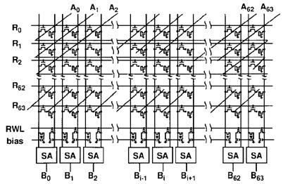
3 GHz Logic with Sense Amplifiers Takahashi, JSSC 5/99 5 Read-out scheme 6 3
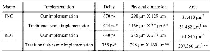
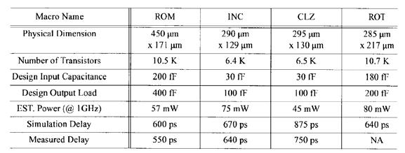
4 Implemented Macros 7 Rotator (ROT) 8 4
 M.")
5 Incrementer (INC) 9 Current-Mode Logic (CML) M. Mizuno, JSSC 6/
6 Current-Mode Logic (CML) 11 Current-Mode Logic (CML) 12 6
7 Optimization for Power The Importance of Power Awareness Crucial for Portable Applications Determines battery lifetime Increased amount of computation Crucial for High-Performance Applications Determines cooling and energy costs Many designs today are power limited Still need maximum performance 14 7


8 The Power Challenge Source: Roger Schmidt IBM Corp K. Yazawa, Sony 15 Mobility: Battery storage the limiting factor Little change in basic technology store energy using a chemical reaction Battery capacity doubles every 10 years Energy density/size, safe handling are limiting factor Energy density KWH/kg of material Gasoline 14 Lead-Acid 0.04 Li polymer

9 Battery Progress First Commercial Use Energy Density (Wh/kg) Trend Line NiCd SLA NiMH Li-Ion Reusable Alkaline Facture 4 over the last 10 years! Li- Polymer 17 Fuel cell may increase stored energy more than a order of magnitude Duration [Hour] Courtesy Toshiba Cellular PDA Lithium Ion Battery Direct Methanol Fuel Cell Note PC Output [W] 18 9


")

10 What can one do with 1 cm 3? Energy Storage Micro Fuel cell Primary battery Secondary battery Ultra-capacitor J/cm µw/cm 3 /year What can one do with 1 cm 3? Energy Generation µw/cm 3 Solar (outside) Air flow Human power Vibration Temperature Pressure Var. Solar (inside) 15,
11 What can one do with 1 cm 3? Reference case: the human brain P avg (brain) = 20 W (20% of the total dissipation, 2% of the weight), Power density: ~15 mw/cm 3 Nerve cells only 4% of brain volume Average neuron density: 70 million/cm 3 21 What can one do with 1 cm 3? Perform computations 300 million 4 input NAND gates (90 nm) 7 million Xilinx gates (90 nm) Assuming 500 MHz clock frequency, 1V Vdd and fanout of 4 and 10% activity: 15 Peta 45 W Reducing supply voltage to 0.2V and clock rate to 10 MHz: 300 Giga 40 mw 22 11
12 Outline 1. Know your enemy: Power consumption in CMOS 2. Leakage is here to stay 3. Power and performance are tightly coupled and have to be jointly optimized 4. Principles of Power Minimization 23 Where does power go in CMOS? Switching power Charging capacitors Leakage power Transistors are imperfect switches Short-circuit power Both pull-up and pull-down on during transition Static currents Biasing currents 1. Know Your Enemy 24 12
13 Dynamic Power Consumption V dd E = C L V DD A 1 PMOS NETWORK i L 1 2 E R = CLVDD 2 A N NMOS NETWORK V out C L 1 2 E C = CLVDD 2 One half of the power from the supply is consumed in the pull-up network and one half is stored on C L Charge from C L is dumped during the 1 0 transition 25 Circuits with Reduced Swing V dd V dd V dd -V Th C L E 0 1 = C V L DD ( V V ) DD Th 26 13
14 Dynamic Power Consumption Power = Energy/transition Transition rate = C L V DD2 f 0 1 = C L V DD2 f P 0 1 = C switched V DD2 f Power dissipation is data dependent depends on the switching probability Switched capacitance C switched = C L P Transition Activity and Power Energy consumed in N cycles, E N : E N = C L V DD2 n 0 1 n 0 1 number of 0 1 transitions in N cycles P avg EN n0 lim f = lim N N N N n0 α 0 1 = lim N N 1 = P avg = α 0 1 C L 1 V C f 2 DD f L V 2 DD f 28 14
15 Type of Logic Function: NOR vs. XOR Example: Static 2-input NOR Gate A B Out If inputs switch every cycle Assume signal probabilities p A=1 = 1/2 p B=1 = 1/2 Then transition probability p 0 1 = p Out=0 x p Out=1 = 3/4 x 1/4 = 3/16 α 0 1 = 3/16 29 Type of Logic Function: NOR vs. XOR A B Example: Static 2-input XOR Gate Out If inputs switch in every cycle Assume signal probabilities p A=1 = 1/2 p B=1 = 1/2 Then transition probability p 0 1 = p Out=0 x p Out=1 = 1/2 x 1/2 = 1/4 α 0 1 = 1/
16 Transition Probabilities P 0->1 (NOR,NAND) = (2 N -1)/2 2N P 0->1 (XOR) = 1/4 31 Transition Probabilities for Basic Gates p 0 1 AND OR XOR (1 - p A p B )p A p B (1 - p A )(1 - p B )(1 - (1 - p A )(1 - p B )) (1 - (p A +p B 2p A p B ))(p A + p B 2p A p B ) Transition probabilities for static CMOS gates p 0 1 = p 0 p
17 Problem: Reconvergent Fanout A X B Z Reconvergence P(Z = 1) = P(B = 1). P(X = 1 B=1) Becomes complex and intractable fast 33 Inter-Signal Correlations A B C Z A C B Z Logic without reconvergent fanout Logic with reconvergent fanout p 0 1 =(1 p A p B ) p A p B P(Z = 1) = p(c=1 B=1) p(b=1) p 0 1 = 0 Need to use conditional probabilities to model inter-signal correlations CAD tools required for such analysis 34 17
18 (V) Voltage Glitching in Static CMOS A X B C Z ABC X Z Gate Delay Also known as dynamic hazards The result is correct, but there is extra power dissipated 35 Example: Chain of NOR Gates 1 Out 1 Out 2 Out 3 Out 4 Out Out 2 Out 6 Out 6 Out Out 1 Out 7 Out 5 Out Time (ps) 36 18
19 (A) I sc Short Circuit Current V DD V DD I sc 0 I sc = I MAX V in C L V out x V in C L V out Large load C L = 20 ff C L = 100 ff Small load C L = 500 ff time (s) Short circuit current is usually well controlled Transistors Leak Drain leakage Diffusion currents Drain-induced barrier lowering Junction leakages Gate-induced drain leakage Gate leakage Tunneling currents through thin oxide 38 19
20 Transistor Leakage -3 V DS = 1.2V -4 G log I DS [log A] S C i C d Sub D -8 Subthreshold slope S = kt/q ln10 (1+C d /C i ) V GS [V] Drain leakage current is exponential with V GS Subthreshold slope is ~70mV/dec 39 Transistor Leakage 8 IDS [na] x in current technologies V DS [V] Two effects: diffusion current (like a bipolar transistor) exponential increase with V DS (DIBL) 40 20
21 Subthreshold Current Subthreshold behavior can be modeled physically Ids V V 2 g Th Vds W kt mkt q kt q = µ e 1 e L q Or simplified to: Ids W = I0 10 W0 ( V V ) gs Th +γvds S 41 From a design perspective Leakage exponential function of VT Leakage dependence upon VDD Initially quite linear Goes up exponentially for larger voltages due to DIBL 42 21
22 Gate Leakage Trends Tunneling at thin oxides Courtesy of IEEE Press, New York Gate Tunneling I GD ~ e Tox e Vgd, I GS ~ e Tox e Vgs V DD Independent of the sub-threshold leakage I SUB Contributes to the total leakage Modeled in BSIM4 V DD I GD 0V Also in BSIM3v3 but foundries usually do not include it I Leak NMOS gate leakage usually worse than PMOS I GS 44 22
23 Power /Energy Optimizaton Space Constant Throughput/Latency Variable Throughput/Latency Energy Design Time Sleep Mode Run Time Logic design Active Scaled V DD TSizing Clock Gating DFS, DVS Multi-V DD Leakage Stack effects + Multi-V T Sleep T s Multi-V DD Variable V T + Input control + Variable V T 45 Reducing active power Downsizing transistors (C L ) Slows down logic Lowering the supply voltage (V DD ) Slows down logic Reducing swing slows down the succeeding stage Pdyn Reducing frequency (f) E Does not reduce energy Reducing switching activity (α) Logic restructuring Reducing glitching Balancing logic ~ α C ~ α C L L V V swing swing V V DD DD f 46 23
24 Relationship Between Power and Delay 2 Power : P = p t f CLK C L V DD + I 0 10 V TH V DD S Delay : D = k C L V DD (V DD - V TH ) 1.3 Power (W) x [From Kuroda] A V DD (V) 2 B V TH (V) Delay (s) x A V DD (V) 2 B V TH (V) -0.4 Power is reduced while delay is unchanged if both V DD and V TH are lowered such as from A to B. 47 Reducing Active Power Downsizing, lowering the supply on the critical path will lower the operating frequency Downsize non-critical paths Narrows down the path delay distribution Increases impact of variations Path count Original delay distribution Target delay Delay 48 24
25 Multi-Level Approach Energy minimization subject to delay constraint Optimal trade-off between energy and area Architecture Micro-Architecture Circuit (Logic & FFs) Energy-Area (Cost) Performance Energy-Performance Energy-Delay 49 Literature Books: J. Rabaey, A. Chandrakasan, B. Nikolic, Digital Integrated Circuits: A Design Perspective, 2 nd ed, Prentice Hall A. Chandrakasan, W. Bowhill, F. Fox (eds.), Design of High-Performance Microprocessor Circuits, IEEE Press Chapter 4, Low-Voltage Technologies, by Kuroda and Sakurai Chapter 3, Techniques for Leakage Power Reduction, by De, et al. A. Chandrakasan and R. Brodersen, Low Power CMOS Design, Kluwer Academic Publishers, J. Rabaey and M. Pedram, Ed., Low Power Design Methodologies, Kluwer Academic Publishers, nd ed, A. Chandrakasan and R. Brodersen, Low-Power CMOS Design, IEEE Press, 1998 (Reprint Volume) 50 25
26 Literature Articles: A. P. Chandrakasan and R. W. Brodersen, Minimizing power consumption in digital CMOS circuits, Proceedings of the IEEE, no.4, p , April A.P. Chandrakasan, S. Sheng, R.W. Brodersen, Low-power CMOS digital design. IEEE Journal of Solid-State Circuits, vol.27, no.4, p , April T.Kuroda, T. Sakurai, Overview of low-power ULSI circuit techniques, IEICE Trans. on Electronics, vol. E78-C, no. 4, pp , April S. Borkar, Design challenges of technology scaling, IEEE Micro, vol.19, no.4, p.23-29, July-Aug
EE241 - Spring 2001 Advanced Digital Integrated Circuits
 EE241 - Spring 21 Advanced Digital Integrated Circuits Lecture 12 Low Power Design Self-Resetting Logic Signals are pulses, not levels 1 Self-Resetting Logic Sense-Amplifying Logic Matsui, JSSC 12/94 2
EE241 - Spring 2000 Advanced Digital Integrated Circuits. Announcements
 EE241 - Spring 2 Advanced Digital Integrated Circuits Lecture 11 Low Power-Low Energy Circuit Design Announcements Homework #2 due Friday, 3/3 by 5pm Midterm project reports due in two weeks - 3/7 by 5pm
CMPEN 411 VLSI Digital Circuits Spring Lecture 14: Designing for Low Power
 CMPEN 411 VLSI Digital Circuits Spring 2012 Lecture 14: Designing for Low Power [Adapted from Rabaey s Digital Integrated Circuits, Second Edition, 2003 J. Rabaey, A. Chandrakasan, B. Nikolic] Sp12 CMPEN
CSE493/593. Designing for Low Power
 CSE493/593 Designing for Low Power Mary Jane Irwin [Adapted from Rabaey s Digital Integrated Circuits, 2002, J. Rabaey et al.].1 Why Power Matters Packaging costs Power supply rail design Chip and system
Lecture 8-1. Low Power Design
 Lecture 8 Konstantinos Masselos Department of Electrical & Electronic Engineering Imperial College London URL: http://cas.ee.ic.ac.uk/~kostas E-mail: k.masselos@ic.ac.uk Lecture 8-1 Based on slides/material
Power Dissipation. Where Does Power Go in CMOS?
 Power Dissipation [Adapted from Chapter 5 of Digital Integrated Circuits, 2003, J. Rabaey et al.] Where Does Power Go in CMOS? Dynamic Power Consumption Charging and Discharging Capacitors Short Circuit
EECS 427 Lecture 11: Power and Energy Reading: EECS 427 F09 Lecture Reminders
 EECS 47 Lecture 11: Power and Energy Reading: 5.55 [Adapted from Irwin and Narayanan] 1 Reminders CAD5 is due Wednesday 10/8 You can submit it by Thursday 10/9 at noon Lecture on 11/ will be taught by
EE115C Winter 2017 Digital Electronic Circuits. Lecture 6: Power Consumption
 EE115C Winter 2017 Digital Electronic Circuits Lecture 6: Power Consumption Four Key Design Metrics for Digital ICs Cost of ICs Reliability Speed Power EE115C Winter 2017 2 Power and Energy Challenges
Objective and Outline. Acknowledgement. Objective: Power Components. Outline: 1) Acknowledgements. Section 4: Power Components
 Acknowledgements. Section 4: Power Components") Objective: Power Components Outline: 1) Acknowledgements 2) Objective and Outline 1 Acknowledgement This lecture note has been obtained from similar courses all over the world. I wish to thank all the
Objective: Power Components Outline: 1) Acknowledgements 2) Objective and Outline 1 Acknowledgement This lecture note has been obtained from similar courses all over the world. I wish to thank all the
Announcements. EE141- Fall 2002 Lecture 7. MOS Capacitances Inverter Delay Power
 - Fall 2002 Lecture 7 MOS Capacitances Inverter Delay Power Announcements Wednesday 12-3pm lab cancelled Lab 4 this week Homework 2 due today at 5pm Homework 3 posted tonight Today s lecture MOS capacitances
Integrated Circuits & Systems
 Federal University of Santa Catarina Center for Technology Computer Science & Electronics Engineering Integrated Circuits & Systems INE 5442 Lecture 14 The CMOS Inverter: dynamic behavior (sizing, inverter
Where Does Power Go in CMOS?
 Power Dissipation Where Does Power Go in CMOS? Dynamic Power Consumption Charging and Discharging Capacitors Short Circuit Currents Short Circuit Path between Supply Rails during Switching Leakage Leaking
Lecture 6 Power Zhuo Feng. Z. Feng MTU EE4800 CMOS Digital IC Design & Analysis 2010
 EE4800 CMOS Digital IC Design & Analysis Lecture 6 Power Zhuo Feng 6.1 Outline Power and Energy Dynamic Power Static Power 6.2 Power and Energy Power is drawn from a voltage source attached to the V DD
EE 466/586 VLSI Design. Partha Pande School of EECS Washington State University
 EE 466/586 VLSI Design Partha Pande School of EECS Washington State University pande@eecs.wsu.edu Lecture 8 Power Dissipation in CMOS Gates Power in CMOS gates Dynamic Power Capacitance switching Crowbar
VLSI Design I; A. Milenkovic 1
 Why Power Matters PE/EE 47, PE 57 VLSI Design I L5: Power and Designing for Low Power Department of Electrical and omputer Engineering University of labama in Huntsville leksandar Milenkovic ( www.ece.uah.edu/~milenka
EE141Microelettronica. CMOS Logic
 Microelettronica CMOS Logic CMOS logic Power consumption in CMOS logic gates Where Does Power Go in CMOS? Dynamic Power Consumption Charging and Discharging Capacitors Short Circuit Currents Short Circuit
Announcements. EE141- Spring 2003 Lecture 8. Power Inverter Chain
 - Spring 2003 Lecture 8 Power Inverter Chain Announcements Homework 3 due today. Homework 4 will be posted later today. Special office hours from :30-3pm at BWRC (in lieu of Tuesday) Today s lecture Power
MOS Transistor Theory
 CHAPTER 3 MOS Transistor Theory Outline 2 1. Introduction 2. Ideal I-V Characteristics 3. Nonideal I-V Effects 4. C-V Characteristics 5. DC Transfer Characteristics 6. Switch-level RC Delay Models MOS
EE5311- Digital IC Design
 EE5311- Digital IC Design Module 1 - The Transistor Janakiraman V Assistant Professor Department of Electrical Engineering Indian Institute of Technology Madras Chennai October 28, 2017 Janakiraman, IITM
MODULE III PHYSICAL DESIGN ISSUES
 VLSI Digital Design MODULE III PHYSICAL DESIGN ISSUES 3.2 Power-supply and clock distribution EE - VDD -P2006 3:1 3.1.1 Power dissipation in CMOS gates Power dissipation importance Package Cost. Power
THE INVERTER. Inverter
 THE INVERTER DIGITAL GATES Fundamental Parameters Functionality Reliability, Robustness Area Performance» Speed (delay)» Power Consumption» Energy Noise in Digital Integrated Circuits v(t) V DD i(t) (a)
COMP 103. Lecture 16. Dynamic Logic
 COMP 03 Lecture 6 Dynamic Logic Reading: 6.3, 6.4 [ll lecture notes are adapted from Mary Jane Irwin, Penn State, which were adapted from Rabaey s Digital Integrated Circuits, 2002, J. Rabaey et al.] COMP03
Design for Manufacturability and Power Estimation. Physical issues verification (DSM)
") Design for Manufacturability and Power Estimation Lecture 25 Alessandra Nardi Thanks to Prof. Jan Rabaey and Prof. K. Keutzer Physical issues verification (DSM) Interconnects Signal Integrity P/G integrity
Design for Manufacturability and Power Estimation Lecture 25 Alessandra Nardi Thanks to Prof. Jan Rabaey and Prof. K. Keutzer Physical issues verification (DSM) Interconnects Signal Integrity P/G integrity
ASIC FPGA Chip hip Design Pow Po e w r e Di ssipation ssipa Mahdi Shabany
 ASIC/FPGA Chip Design Power Di ssipation Mahdi Shabany Department tof Electrical ti lengineering i Sharif University of technology Outline Introduction o Dynamic Power Dissipation Static Power Dissipation
EECS150 - Digital Design Lecture 22 Power Consumption in CMOS. Announcements
 EECS150 - Digital Design Lecture 22 Power Consumption in CMOS November 22, 2011 Elad Alon Electrical Engineering and Computer Sciences University of California, Berkeley http://www-inst.eecs.berkeley.edu/~cs150
Last Lecture. Power Dissipation CMOS Scaling. EECS 141 S02 Lecture 8
 EECS 141 S02 Lecture 8 Power Dissipation CMOS Scaling Last Lecture CMOS Inverter loading Switching Performance Evaluation Design optimization Inverter Sizing 1 Today CMOS Inverter power dissipation» Dynamic»
Digital Integrated Circuits A Design Perspective
 Digital Integrated Circuits Design Perspective Designing Combinational Logic Circuits Fuyuzhuo School of Microelectronics,SJTU Introduction Digital IC Dynamic Logic Introduction Digital IC 2 EE141 Dynamic
DKDT: A Performance Aware Dual Dielectric Assignment for Tunneling Current Reduction
 DKDT: A Performance Aware Dual Dielectric Assignment for Tunneling Current Reduction Saraju P. Mohanty Dept of Computer Science and Engineering University of North Texas smohanty@cs.unt.edu http://www.cs.unt.edu/~smohanty/
The Devices. Digital Integrated Circuits A Design Perspective. Jan M. Rabaey Anantha Chandrakasan Borivoje Nikolic. July 30, 2002
 Digital Integrated Circuits A Design Perspective Jan M. Rabaey Anantha Chandrakasan Borivoje Nikolic The Devices July 30, 2002 Goal of this chapter Present intuitive understanding of device operation Introduction
CMPEN 411 VLSI Digital Circuits Spring 2011 Lecture 07: Pass Transistor Logic
 CMPEN 411 VLSI Digital Circuits Spring 2011 Lecture 07: Pass Transistor Logic [dapted from Rabaey s Digital Integrated Circuits, Second Edition, 2003 J. Rabaey,. Chandrakasan,. Nikolic] Sp11 CMPEN 411
ESE 570: Digital Integrated Circuits and VLSI Fundamentals
 ESE 570: Digital Integrated Circuits and VLSI Fundamentals Lec 15: March 15, 2018 Euler Paths, Energy Basics and Optimization Midterm! Midterm " Mean: 89.7 " Standard Dev: 8.12 2 Lecture Outline! Euler
Status. Embedded System Design and Synthesis. Power and temperature Definitions. Acoustic phonons. Optic phonons
 Status http://robertdick.org/esds/ Office: EECS 2417-E Department of Electrical Engineering and Computer Science University of Michigan Specification, languages, and modeling Computational complexity,
Digital Integrated Circuits Designing Combinational Logic Circuits. Fuyuzhuo
 Digital Integrated Circuits Designing Combinational Logic Circuits Fuyuzhuo Introduction Digital IC Dynamic Logic Introduction Digital IC EE141 2 Dynamic logic outline Dynamic logic principle Dynamic logic
Midterm. ESE 570: Digital Integrated Circuits and VLSI Fundamentals. Lecture Outline. Pass Transistor Logic. Restore Output.
 ESE 570: Digital Integrated Circuits and VLSI Fundamentals Lec 16: March 21, 2017 Transmission Gates, Euler Paths, Energy Basics Review Midterm! Midterm " Mean: 79.5 " Standard Dev: 14.5 2 Lecture Outline!
ESE570 Spring University of Pennsylvania Department of Electrical and System Engineering Digital Integrated Cicruits AND VLSI Fundamentals
 University of Pennsylvania Department of Electrical and System Engineering Digital Integrated Cicruits AND VLSI Fundamentals ESE570, Spring 017 Final Wednesday, May 3 4 Problems with point weightings shown.
Lecture 7 Circuit Delay, Area and Power
 Lecture 7 Circuit Delay, Area and Power lecture notes from S. Mitra Intro VLSI System course (EE271) Introduction to VLSI Systems 1 Circuits and Delay Introduction to VLSI Systems 2 Power, Delay and Area:
Dynamic operation 20
 Dynamic operation 20 A simple model for the propagation delay Symmetric inverter (rise and fall delays are identical) otal capacitance is linear t p Minimum length devices R W C L t = 0.69R C = p W L 0.69
ECE 546 Lecture 10 MOS Transistors
 ECE 546 Lecture 10 MOS Transistors Spring 2018 Jose E. Schutt-Aine Electrical & Computer Engineering University of Illinois jesa@illinois.edu NMOS Transistor NMOS Transistor N-Channel MOSFET Built on p-type
EECS 141: FALL 05 MIDTERM 1
 University of California College of Engineering Department of Electrical Engineering and Computer Sciences D. Markovic TuTh 11-1:3 Thursday, October 6, 6:3-8:pm EECS 141: FALL 5 MIDTERM 1 NAME Last SOLUTION
Lecture 2: CMOS technology. Energy-aware computing
 Energy-Aware Computing Lecture 2: CMOS technology Basic components Transistors Two types: NMOS, PMOS Wires (interconnect) Transistors as switches Gate Drain Source NMOS: When G is @ logic 1 (actually over
Integrated Circuits & Systems
 Federal University of Santa Catarina Center for Technology Computer Science & Electronics Engineering Integrated Circuits & Systems INE 5442 Lecture 16 CMOS Combinational Circuits - 2 guntzel@inf.ufsc.br
Chapter 5. The Inverter. V1. April 10, 03 V1.1 April 25, 03 V2.1 Nov Inverter
 Chapter 5 The Inverter V1. April 10, 03 V1.1 April 25, 03 V2.1 Nov.12 03 Objective of This Chapter Use Inverter to know basic CMOS Circuits Operations Watch for performance Index such as Speed (Delay calculation)
EE 466/586 VLSI Design. Partha Pande School of EECS Washington State University
 EE 466/586 VLSI Design Partha Pande School of EECS Washington State University pande@eecs.wsu.edu Lecture 9 Propagation delay Power and delay Tradeoffs Follow board notes Propagation Delay Switching Time
Miscellaneous Lecture topics. Mary Jane Irwin [Adapted from Rabaey s Digital Integrated Circuits, 2002, J. Rabaey et al.]
![Miscellaneous Lecture topics. Mary Jane Irwin [Adapted from Rabaey s Digital Integrated Circuits, 2002, J. Rabaey et al.]](/thumbs/81/84503671.jpg "Miscellaneous Lecture topics. Mary Jane Irwin [Adapted from Rabaey s Digital Integrated Circuits, 2002, J. Rabaey et al.]") Miscellaneous Lecture topics Mary Jane Irwin [dapted from Rabaey s Digital Integrated Circuits, 2002, J. Rabaey et al.] MOS Switches MOS transistors can be viewed as simple switches. In an N-Switch, the
Miscellaneous Lecture topics Mary Jane Irwin [dapted from Rabaey s Digital Integrated Circuits, 2002, J. Rabaey et al.] MOS Switches MOS transistors can be viewed as simple switches. In an N-Switch, the
ESE 570: Digital Integrated Circuits and VLSI Fundamentals
 ESE 570: Digital Integrated Circuits and VLSI Fundamentals Lec 17: March 26, 2019 Energy Optimization & Design Space Exploration Penn ESE 570 Spring 2019 Khanna Lecture Outline! Energy Optimization! Design
Digital Integrated Circuits A Design Perspective
 Semiconductor Memories Adapted from Chapter 12 of Digital Integrated Circuits A Design Perspective Jan M. Rabaey et al. Copyright 2003 Prentice Hall/Pearson Outline Memory Classification Memory Architectures
ΗΜΥ 307 ΨΗΦΙΑΚΑ ΟΛΟΚΛΗΡΩΜΕΝΑ ΚΥΚΛΩΜΑΤΑ Εαρινό Εξάμηνο 2018
 ΗΜΥ 307 ΨΗΦΙΑΚΑ ΟΛΟΚΛΗΡΩΜΕΝΑ ΚΥΚΛΩΜΑΤΑ Εαρινό Εξάμηνο 2018 ΔΙΑΛΕΞΗ 11: Dynamic CMOS Circuits ΧΑΡΗΣ ΘΕΟΧΑΡΙΔΗΣ (ttheocharides@ucy.ac.cy) (ack: Prof. Mary Jane Irwin and Vijay Narayanan) [Προσαρμογή από
EE5311- Digital IC Design
 EE5311- Digital IC Design Module 3 - The Inverter Janakiraman V Assistant Professor Department of Electrical Engineering Indian Institute of Technology Madras Chennai September 3, 2018 Janakiraman, IITM
Nanometer Transistors and Their Models. Jan M. Rabaey
 Nanometer Transistors and Their Models Jan M. Rabaey Chapter Outline Nanometer transistor behavior and models Sub-threshold currents and leakage Variability Device and technology innovations Nanometer
τ gd =Q/I=(CV)/I I d,sat =(µc OX /2)(W/L)(V gs -V TH ) 2 ESE534 Computer Organization Today At Issue Preclass 1 Energy and Delay Tradeoff
/I I d,sat =(µc OX /2)(W/L)(V gs -V TH ) 2 ESE534 Computer Organization Today At Issue Preclass 1 Energy and Delay Tradeoff") ESE534 Computer Organization Today Day 8: February 10, 2010 Energy, Power, Reliability Energy Tradeoffs? Voltage limits and leakage? Variations Transients Thermodynamics meets Information Theory (brief,
ESE534 Computer Organization Today Day 8: February 10, 2010 Energy, Power, Reliability Energy Tradeoffs? Voltage limits and leakage? Variations Transients Thermodynamics meets Information Theory (brief,
Lecture 12 Digital Circuits (II) MOS INVERTER CIRCUITS
 MOS INVERTER CIRCUITS") Lecture 12 Digital Circuits (II) MOS INVERTER CIRCUITS Outline NMOS inverter with resistor pull-up The inverter NMOS inverter with current-source pull-up Complementary MOS (CMOS) inverter Static analysis
Lecture 12 Digital Circuits (II) MOS INVERTER CIRCUITS Outline NMOS inverter with resistor pull-up The inverter NMOS inverter with current-source pull-up Complementary MOS (CMOS) inverter Static analysis
L ECE 4211 UConn F. Jain Scaling Laws for NanoFETs Chapter 10 Logic Gate Scaling
 L13 04202017 ECE 4211 UConn F. Jain Scaling Laws for NanoFETs Chapter 10 Logic Gate Scaling Scaling laws: Generalized scaling (GS) p. 610 Design steps p.613 Nanotransistor issues (page 626) Degradation
Lecture Outline. ESE 570: Digital Integrated Circuits and VLSI Fundamentals. Review: 1st Order RC Delay Models. Review: Two-Input NOR Gate (NOR2)
") ESE 570: Digital Integrated Circuits and VLSI Fundamentals Lec 14: March 1, 2016 Combination Logic: Ratioed and Pass Logic Lecture Outline! CMOS Gates Review " CMOS Worst Case Analysis! Ratioed Logic Gates!
ESE 570: Digital Integrated Circuits and VLSI Fundamentals Lec 14: March 1, 2016 Combination Logic: Ratioed and Pass Logic Lecture Outline! CMOS Gates Review " CMOS Worst Case Analysis! Ratioed Logic Gates!
EE241 - Spring 2003 Advanced Digital Integrated Circuits
 EE241 - Spring 2003 Advanced Digital Integrated Circuits Lecture 16 Energy-Recovery Circuits SOI Technology and Circuits Optimal EDP Contours 1 Leakage and Switching ELk 2 = ESw Opt L ln d K tech α avg
The Physical Structure (NMOS)
") The Physical Structure (NMOS) Al SiO2 Field Oxide Gate oxide S n+ Polysilicon Gate Al SiO2 SiO2 D n+ L channel P Substrate Field Oxide contact Metal (S) n+ (G) L W n+ (D) Poly 1 Transistor Resistance Two
The Physical Structure (NMOS) Al SiO2 Field Oxide Gate oxide S n+ Polysilicon Gate Al SiO2 SiO2 D n+ L channel P Substrate Field Oxide contact Metal (S) n+ (G) L W n+ (D) Poly 1 Transistor Resistance Two
ESE 570: Digital Integrated Circuits and VLSI Fundamentals
 ESE 570: Digital Integrated Circuits and VLSI Fundamentals Lec 17: March 23, 2017 Energy and Power Optimization, Design Space Exploration, Synchronous MOS Logic Lecture Outline! Energy and Power Optimization
Dynamic Combinational Circuits. Dynamic Logic
 Dynamic Combinational Circuits Dynamic circuits Charge sharing, charge redistribution Domino logic np-cmos (zipper CMOS) Krish Chakrabarty 1 Dynamic Logic Dynamic gates use a clocked pmos pullup Two modes:
CPE/EE 427, CPE 527 VLSI Design I L18: Circuit Families. Outline
 CPE/EE 47, CPE 57 VLI Design I L8: Circuit Families Department of Electrical and Computer Engineering University of labama in Huntsville leksandar Milenkovic ( www.ece.uah.edu/~milenka ) www.ece.uah.edu/~milenka/cpe57-05f
EEC 118 Lecture #5: CMOS Inverter AC Characteristics. Rajeevan Amirtharajah University of California, Davis Jeff Parkhurst Intel Corporation
 EEC 8 Lecture #5: CMOS Inverter AC Characteristics Rajeevan Amirtharajah University of California, Davis Jeff Parkhurst Intel Corporation Acknowledgments Slides due to Rajit Manohar from ECE 547 Advanced
Digital Integrated Circuits A Design Perspective
 Digital Integrated Circuits Design Perspective Jan M. Rabaey nantha Chandrakasan orivoje Nikolić Designing Combinational Logic Circuits November 2002. 1 Combinational vs. Sequential Logic In Combinational
Digital Integrated Circuits A Design Perspective. Jan M. Rabaey Anantha Chandrakasan Borivoje Nikolic. The Devices. July 30, Devices.
 Digital Integrated Circuits A Design Perspective Jan M. Rabaey Anantha Chandrakasan Borivoje Nikolic The July 30, 2002 1 Goal of this chapter Present intuitive understanding of device operation Introduction
CMPEN 411 VLSI Digital Circuits. Lecture 03: MOS Transistor
 CMPEN 411 VLSI Digital Circuits Lecture 03: MOS Transistor Kyusun Choi [Adapted from Rabaey s Digital Integrated Circuits, Second Edition, 2003 J. Rabaey, A. Chandrakasan, B. Nikolic] CMPEN 411 L03 S.1
CMPEN 411 VLSI Digital Circuits. Lecture 04: CMOS Inverter (static view)
") CMPEN 411 VLSI Digital Circuits Lecture 04: CMOS Inverter (static view) Kyusun Choi [Adapted from Rabaey s Digital Integrated Circuits, Second Edition, 2003 J. Rabaey, A. Chandrakasan, B. Nikolic] CMPEN
CMPEN 411 VLSI Digital Circuits Lecture 04: CMOS Inverter (static view) Kyusun Choi [Adapted from Rabaey s Digital Integrated Circuits, Second Edition, 2003 J. Rabaey, A. Chandrakasan, B. Nikolic] CMPEN
DC and Transient Responses (i.e. delay) (some comments on power too!)
 (some comments on power too!)") DC and Transient Responses (i.e. delay) (some comments on power too!) Michael Niemier (Some slides based on lecture notes by David Harris) 1 Lecture 02 - CMOS Transistor Theory & the Effects of Scaling
DC and Transient Responses (i.e. delay) (some comments on power too!) Michael Niemier (Some slides based on lecture notes by David Harris) 1 Lecture 02 - CMOS Transistor Theory & the Effects of Scaling
EEC 118 Lecture #2: MOSFET Structure and Basic Operation. Rajeevan Amirtharajah University of California, Davis Jeff Parkhurst Intel Corporation
 EEC 118 Lecture #2: MOSFET Structure and Basic Operation Rajeevan Amirtharajah University of California, Davis Jeff Parkhurst Intel Corporation Announcements Lab 1 this week, report due next week Bring
Subthreshold Operated CMOS Analytic Model
 IX Symposium Industrial Electronics INDEL 2012, Banja Luka, November 0103, 2012 Subthreshold Operated CMOS Analytic Model Branko Dokic Faculty of Electrical Engineering University of Banja Luka bdokic@etfbl.net
ESE 570: Digital Integrated Circuits and VLSI Fundamentals
 ESE 570: Digital Integrated Circuits and VLSI Fundamentals Lec 18: March 27, 2018 Dynamic Logic, Charge Injection Lecture Outline! Sequential MOS Logic " D-Latch " Timing Constraints! Dynamic Logic " Domino
Pass-Transistor Logic
 -all 26 Digital tegrated ircuits nnouncements No new homework this week roject phase one due on Monday Midterm 2 next Thursday Review session on Tuesday Lecture 8 Logic Dynamic Logic EE4 EE4 2 lass Material
Lecture 5: CMOS Transistor Theory
 Lecture 5: CMOS Transistor Theory Slides courtesy of Deming Chen Slides based on the initial set from David Harris CMOS VLSI Design Outline q q q q q q q Introduction MOS Capacitor nmos I-V Characteristics
Topic 4. The CMOS Inverter
 Topic 4 The CMOS Inverter Peter Cheung Department of Electrical & Electronic Engineering Imperial College London URL: www.ee.ic.ac.uk/pcheung/ E-mail: p.cheung@ic.ac.uk Topic 4-1 Noise in Digital Integrated
Lecture 12 Circuits numériques (II)
") Lecture 12 Circuits numériques (II) Circuits inverseurs MOS Outline NMOS inverter with resistor pull-up The inverter NMOS inverter with current-source pull-up Complementary MOS (CMOS) inverter Static analysis
Lecture 12 Circuits numériques (II) Circuits inverseurs MOS Outline NMOS inverter with resistor pull-up The inverter NMOS inverter with current-source pull-up Complementary MOS (CMOS) inverter Static analysis
Lecture 4: CMOS review & Dynamic Logic
 Lecture 4: CMOS review & Dynamic Logic Reading: ch5, ch6 Overview CMOS basics Power and energy in CMOS Dynamic logic 1 CMOS Properties Full rail-to-rail swing high noise margins Logic levels not dependent
Fig. 1 CMOS Transistor Circuits (a) Inverter Out = NOT In, (b) NOR-gate C = NOT (A or B)
 Inverter Out = NOT In, (b) NOR-gate C = NOT (A or B)") 1 Introduction to Transistor-Level Logic Circuits 1 By Prawat Nagvajara At the transistor level of logic circuits, transistors operate as switches with the logic variables controlling the open or closed
1 Introduction to Transistor-Level Logic Circuits 1 By Prawat Nagvajara At the transistor level of logic circuits, transistors operate as switches with the logic variables controlling the open or closed
Lecture Outline. ESE 570: Digital Integrated Circuits and VLSI Fundamentals. Total Power. Energy and Power Optimization. Worksheet Problem 1
 ESE 570: Digital Integrated Circuits and VLSI Fundamentals Lec 16: March 20, 2018 Energy and Power Optimization, Design Space Exploration Lecture Outline! Energy and Power Optimization " Tradeoffs! Design
EE 330 Lecture 37. Digital Circuits. Other Logic Families. Propagation Delay basic characterization Device Sizing (Inverter and multiple-input gates)
") EE 330 Lecture 37 Digital Circuits Other Logic Families Static Power Dissipation Propagation Delay basic characterization Device Sizing (Inverter and multiple-input gates) Review from Last Time Inverter
EE 330 Lecture 37 Digital Circuits Other Logic Families Static Power Dissipation Propagation Delay basic characterization Device Sizing (Inverter and multiple-input gates) Review from Last Time Inverter
Dynamic Combinational Circuits. Dynamic Logic
 Dynamic Combinational Circuits Dynamic circuits Charge sharing, charge redistribution Domino logic np-cmos (zipper CMOS) Krish Chakrabarty 1 Dynamic Logic Dynamic gates use a clocked pmos pullup Two modes:
CMOS INVERTER. Last Lecture. Metrics for qualifying digital circuits. »Cost» Reliability» Speed (delay)»performance
»performance") CMOS INVERTER Last Lecture Metrics for qualifying digital circuits»cost» Reliability» Speed (delay)»performance 1 Today s lecture The CMOS inverter at a glance An MOS transistor model for manual analysis
CMOS INVERTER Last Lecture Metrics for qualifying digital circuits»cost» Reliability» Speed (delay)»performance 1 Today s lecture The CMOS inverter at a glance An MOS transistor model for manual analysis
EE 434 Lecture 33. Logic Design
 EE 434 Lecture 33 Logic Design Review from last time: Ask the inverter how it will interpret logic levels V IN V OUT V H =? V L =? V LARGE V H V L V H Review from last time: The two-inverter loop X Y X
EECS 141 F01 Lecture 17
 EECS 4 F0 Lecture 7 With major inputs/improvements From Mary-Jane Irwin (Penn State) Dynamic CMOS In static circuits at every point in time (except when switching) the output is connected to either GND
MASSACHUSETTS INSTITUTE OF TECHNOLOGY Department of Electrical Engineering and Computer Sciences
 MSSCHUSETTS INSTITUTE OF TECHNOLOGY Department of Electrical Engineering and Computer Sciences nalysis and Design of Digital Integrated Circuits (6.374) - Fall 2003 Quiz #1 Prof. nantha Chandrakasan Student
Switching circuits: basics and switching speed
 ECE137B notes; copyright 2018 Switching circuits: basics and switching speed Mark Rodwell, University of California, Santa Barbara Amplifiers vs. switching circuits Some transistor circuit might have V
Impact of Scaling on The Effectiveness of Dynamic Power Reduction Schemes
 Impact of Scaling on The Effectiveness of Dynamic Power Reduction Schemes D. Duarte Intel Corporation david.e.duarte@intel.com N. Vijaykrishnan, M.J. Irwin, H-S Kim Department of CSE, Penn State University
Lecture 29 - The Long Metal-Oxide-Semiconductor Field-Effect Transistor (cont.) April 20, 2007
 April 20, 2007") 6.720J/3.43J - Integrated Microelectronic Devices - Spring 2007 Lecture 29-1 Lecture 29 - The Long Metal-Oxide-Semiconductor Field-Effect Transistor (cont.) April 20, 2007 Contents: 1. Non-ideal and second-order
6.720J/3.43J - Integrated Microelectronic Devices - Spring 2007 Lecture 29-1 Lecture 29 - The Long Metal-Oxide-Semiconductor Field-Effect Transistor (cont.) April 20, 2007 Contents: 1. Non-ideal and second-order
Semiconductor Memories
 Semiconductor References: Adapted from: Digital Integrated Circuits: A Design Perspective, J. Rabaey UCB Principles of CMOS VLSI Design: A Systems Perspective, 2nd Ed., N. H. E. Weste and K. Eshraghian
Lecture 6: Circuit design part 1
 Lecture 6: Circuit design part 6. Combinational circuit design 6. Sequential circuit design 6.3 Circuit simulation 6.4. Hardware description language Combinational Circuit Design. Combinational circuit
CSE140L: Components and Design Techniques for Digital Systems Lab. Power Consumption in Digital Circuits. Pietro Mercati
 CSE140L: Components and Design Techniques for Digital Systems Lab Power Consumption in Digital Circuits Pietro Mercati 1 About the final Friday 09/02 at 11.30am in WLH2204 ~2hrs exam including (but not
Lecture 27: Latches. Final presentations May 8, 1-5pm, BWRC Final reports due May 7 Final exam, Monday, May :30pm, 241 Cory
 EE241 - Spring 2008 Advanced Digital Integrated Circuits Lecture 27: Latches Timing Announcements Wrapping-up the class: Final presentations May 8, 1-5pm, BWRC Final reports due May 7 Final exam, Monday,
Integrated Circuits & Systems
 Federal University of Santa Catarina Center for Technology Computer Science & Electronics Engineering Integrated Circuits & Systems INE 5442 Lecture 12 The CMOS Inverter: static behavior guntzel@inf.ufsc.br
Lecture 14: Circuit Families
 Introduction to CMOS VLSI Design Lecture 4: Circuit Families David Harris, Harvey Mudd College Kartik Mohanram and Steven Levitan University of Pittsburgh Outline q Pseudo-nMOS Logic q Dynamic Logic q
MOSFET and CMOS Gate. Copy Right by Wentai Liu
 MOSFET and CMOS Gate CMOS Inverter DC Analysis - Voltage Transfer Curve (VTC) Find (1) (2) (3) (4) (5) (6) V OH min, V V OL min, V V IH min, V V IL min, V OHmax OLmax IHmax ILmax NM L = V ILmax V OL max
Semiconductor Memories
 !"#"$%&'()$*#+%$*,' -"+./"$0 1'!*0"#)'2*+03*.$"4* Jan M. Rabaey Anantha Chandrakasan Borivoje Nikolic Semiconductor Memories December 20, 2002 !"#$%&'()*&'*+&, Memory Classification Memory Architectures
! Charge Leakage/Charge Sharing. " Domino Logic Design Considerations. ! Logic Comparisons. ! Memory. " Classification. " ROM Memories.
 ESE 57: Digital Integrated Circuits and VLSI Fundamentals Lec 9: March 9, 8 Memory Overview, Memory Core Cells Today! Charge Leakage/ " Domino Logic Design Considerations! Logic Comparisons! Memory " Classification
L2: Combinational Logic Design (Construction and Boolean Algebra)
") L2: Combinational Logic Design (Construction and Boolean Algebra) Acknowledgements: Lecture material adapted from Chapter 2 of R. Katz, G. Borriello, Contemporary Logic Design (second edition), Pearson
L2: Combinational Logic Design (Construction and Boolean Algebra) Acknowledgements: Lecture material adapted from Chapter 2 of R. Katz, G. Borriello, Contemporary Logic Design (second edition), Pearson
Topics. Dynamic CMOS Sequential Design Memory and Control. John A. Chandy Dept. of Electrical and Computer Engineering University of Connecticut
 Topics Dynamic CMOS Sequential Design Memory and Control Dynamic CMOS In static circuits at every point in time (except when switching) the output is connected to either GND or V DD via a low resistance
COMP 103. Lecture 10. Inverter Dynamics: The Quest for Performance. Section 5.4.2, What is this lecture+ about? PERFORMANCE
 COMP 103 Lecture 10 Inverter Dynamics: The Quest for Performance Section 5.4.2, 5.4.3 [All lecture notes are adapted from Mary Jane Irwin, Penn State, which were adapted from Rabaey s Digital Integrated
Digital Integrated Circuits A Design Perspective
 igital Integrated Circuits esign Perspective esigning Combinational Logic Circuits 1 Combinational vs. Sequential Logic In Combinational Logic Circuit Out In Combinational Logic Circuit Out State Combinational
Lecture 11: MOSFET Modeling
 Digital Integrated Circuits (83-313) Lecture 11: MOSFET ing Semester B, 2016-17 Lecturer: Dr. Adam Teman TAs: Itamar Levi, Robert Giterman 18 June 2017 Disclaimer: This course was prepared, in its entirety,
EE115C Digital Electronic Circuits Homework #4
 EE115 Digital Electronic ircuits Homework #4 Problem 1 Power Dissipation Solution Vdd =1.0V onsider the source follower circuit used to drive a load L =20fF shown above. M1 and M2 are both NMOS transistors
9/18/2008 GMU, ECE 680 Physical VLSI Design
 ECE680: Physical VLSI Design Chapter III CMOS Device, Inverter, Combinational circuit Logic and Layout Part 3 Combinational Logic Gates (textbook chapter 6) 9/18/2008 GMU, ECE 680 Physical VLSI Design
L16: Power Dissipation in Digital Systems. L16: Spring 2007 Introductory Digital Systems Laboratory
 L16: Power Dissipation in Digital Systems 1 Problem #1: Power Dissipation/Heat Power (Watts) 100000 10000 1000 100 10 1 0.1 4004 80088080 8085 808686 386 486 Pentium proc 18KW 5KW 1.5KW 500W 1971 1974