Announcements. EE141- Fall 2002 Lecture 7. MOS Capacitances Inverter Delay Power
|
|
|
- Lesley Foster
- 5 years ago
- Views:
Transcription
1 - Fall 2002 Lecture 7 MOS Capacitances Inverter Delay Power Announcements Wednesday 12-3pm lab cancelled Lab 4 this week Homework 2 due today at 5pm Homework 3 posted tonight
2 Today s lecture MOS capacitances Inverter propagation delay Power consumption MOS Capacitances Dynamic Behavior
3 Dynamic Behavior of MOS Transistor G C GS C GD S D C SB C GB C DB B The Gate Capacitance
4 Gate Capacitance G G G S C GC C GC C GC D S D S D Cut-off Resistive Saturation Most important regions in digital design: saturation and cut-off Gate Capacitance WLC ox C GC WLC ox C GC WLC ox 2 C GC B C GCS = C GCD WLC ox 2 C GCS C GCD 2WLC ox 3 V GS 0 V DS /(V GS -V T ) 1 Capacitance as a function of VGS (with VDS = 0) Capacitance as a function of the degree of saturation
5 Diffusion Capacitance Junction Capacitance
6 Linearizing the Junction Capacitance Replace non-linear capacitance by large-signal equivalent linear capacitance which displaces equal charge over voltage swing of interest Capacitances in 0.25 µm CMOS process
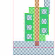
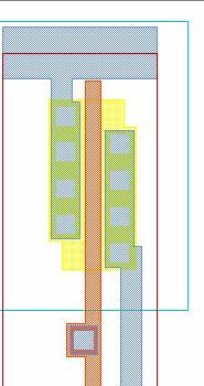
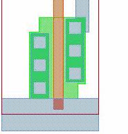
7 .MODEL Parameters MOS1.MODEL Modname NMOS/PMOS <VTO=VTO...> Computing the Capacitances V DD V DD V in C gd12 M2 C db2 V out C g4 M4 V out2 M1 C db1 C w Interconnect C g3 M3 Fanout Simplified Model V in V out C L
8 The Miller Effect V C gd1 V out V out V V in V 2C gd1 M1 V V in M1 A capacitor experiencing identical but opposite voltage swings at both its terminals can be replaced by a capacitor to ground, whose value is two times the original value. Computing the Capacitances

9 CMOS Inverters V DD Propagation Delay
10 CMOS Inverter Propagation Delay Approach 1 V DD t phl = C L V swing /2 I av V out ~ C L I av C L k n V DD V in = V DD CMOS Inverter Propagation Delay Approach 2 V DD t phl = f(r on.c L ) = 0.69 R on C L V out V out ln(0.5) R on C L 1 V DD V in = V DD R on C L t
11 3 2.5? Transient Response V out (V) t plh t phl t p = 0.69 C L (R eqn +R eqp )/ t (sec) x Design for Performance Keep capacitances small Increase transistor sizes» watch out for self-loading! Increase V DD (?)
12 Delay as a function of V DD t p (normalized) V (V) DD Device Sizing 3.8 x (for fixed load) t p (sec) Self-loading effect: Intrinsic capacitances dominate S
13 NMOS/PMOS ratio 5 x tplh tphl 4.5 t p (sec) 4 tp β = W p /W n β Impact of Rise Time on Delay t phl (nsec) t rise (nsec) t p = t step(i) + ηt step(i-1)
14 The Sub-Micron MOS Transistor Threshold Variations Subthreshold Conduction Parasitic Resistances Threshold Variations V T V T Long-channel threshold Low V DS threshold Threshold as a function of the length (for low V DS ) L V DS Drain-induced barrier lowering (for low L)
15 Sub-Threshold Conduction I D (A) Quadratic Linear The Slope Factor I D ~ I 0 e qvgs nkt, C n =1+ C S is V GS for I D2 /I D1 =10 D ox Exponential V T V GS (V) Typical values for S: mv/decade Sub-Threshold I D vs V GS qvgs nkt I D I0e 1 e qvds = kt V DS from 0 to 0.5V
 DS V GS from 0 to 0.")
16 Sub-Threshold I D vs V DS I D qvgs qvds = nkt kt I e 0 1 e ( 1+ λ V ) DS V GS from 0 to 0.3V Power Dissipation
17 Where Does Power Go in CMOS? Dynamic Power Consumption Charging and Discharging Capacitors Short Circuit Currents Short Circuit Path between Supply Rails during Switching Leakage Leaking diodes and transistors Dynamic Power Dissipation Vdd Vin Vout C L Energy/transition = C L * V dd 2 Power = Energy/transition * f = C L * V dd 2 * f Not a function of transistor sizes! Need to reduce C L, V dd, and f to reduce power.
18 Modification for Circuits with Reduced Swing V dd V dd V dd -V t C L E 0 1 = C L V dd ( V dd V t ) Can exploit reduced swing to lower power (e.g., reduced bit-line swing in memory) Adiabatic Charging 2 2 2
19 Adiabatic Charging Node Transition Activity and Power Consider switching a CMOS gate for N clock cycles E = C V N L 2 nn dd ( ) E N : the energy consumed for N clock cycles n(n): the number of 0->1 transition in N clock cycles P = lim avg N E N f N clk = nn ( ) lim C N N L V 2 fclk dd α 0 1 = nn ( ) lim N N P avg = α 0 1 C L V 2 fclk dd
20 Short Circuit Currents Vd d Vin Vout C L 0.15 I VDD (ma) V in (V) How to keep Short-Circuit Currents Down? Short circuit current goes to zero if t fall >> t rise, but can t do this for cascade logic, so...
21 Minimizing Short-Circuit Power Vdd =3.3 rm P no Vdd = Vdd = t sin /t sout Leakage Vdd Vout Drain Junction Leakage Sub-Threshold Current Sub-threshold current one of most compelling issues in low-energy circuit design!
22 Reverse-Biased Diode Leakage GATE p + p+ N Reverse Leakage Current + - V dd I DL = J S A JS = pa/µm2 at 25 deg C for 0.25µm CMOS JS doubles for every 9 deg C! Subthreshold Leakage Component
23 Static Power Consumption Vdd I stat V out V in =5V C L P stat = P (In=1).V dd. I stat Wasted energy Should be avoided in most cases, but could help reducing energy in others (e.g. sense amps) Principles for Power Reduction Prime choice: Reduce voltage!» Recent years have seen an acceleration in supply voltage reduction» Design at very low voltages still open question ( V by 2010!) Reduce switching activity Reduce physical capacitance» Device Sizing: for F=20 f opt (energy)=3.53, f opt (performance)=4.47
Power Dissipation. Where Does Power Go in CMOS?
 Power Dissipation [Adapted from Chapter 5 of Digital Integrated Circuits, 2003, J. Rabaey et al.] Where Does Power Go in CMOS? Dynamic Power Consumption Charging and Discharging Capacitors Short Circuit
Last Lecture. Power Dissipation CMOS Scaling. EECS 141 S02 Lecture 8
 EECS 141 S02 Lecture 8 Power Dissipation CMOS Scaling Last Lecture CMOS Inverter loading Switching Performance Evaluation Design optimization Inverter Sizing 1 Today CMOS Inverter power dissipation» Dynamic»
Announcements. EE141- Spring 2003 Lecture 8. Power Inverter Chain
 - Spring 2003 Lecture 8 Power Inverter Chain Announcements Homework 3 due today. Homework 4 will be posted later today. Special office hours from :30-3pm at BWRC (in lieu of Tuesday) Today s lecture Power
Check course home page periodically for announcements. Homework 2 is due TODAY by 5pm In 240 Cory
 EE141 Fall 005 Lecture 6 MOS Capacitances, Propagation elay Important! Check course home page periodically for announcements Homework is due TOAY by 5pm In 40 Cory Homework 3 will be posted TOAY ue Thursday
THE INVERTER. Inverter
 THE INVERTER DIGITAL GATES Fundamental Parameters Functionality Reliability, Robustness Area Performance» Speed (delay)» Power Consumption» Energy Noise in Digital Integrated Circuits v(t) V DD i(t) (a)
Digital Integrated Circuits 2nd Inverter
 Digital Integrated Circuits The Inverter The CMOS Inverter V DD Analysis Inverter complex gate Cost V in V out complexity & Area Integrity and robustness C L Static behavior Performance Dynamic response
Where Does Power Go in CMOS?
 Power Dissipation Where Does Power Go in CMOS? Dynamic Power Consumption Charging and Discharging Capacitors Short Circuit Currents Short Circuit Path between Supply Rails during Switching Leakage Leaking
EE 466/586 VLSI Design. Partha Pande School of EECS Washington State University
 EE 466/586 VLSI Design Partha Pande School of EECS Washington State University pande@eecs.wsu.edu Lecture 8 Power Dissipation in CMOS Gates Power in CMOS gates Dynamic Power Capacitance switching Crowbar
Chapter 5. The Inverter. V1. April 10, 03 V1.1 April 25, 03 V2.1 Nov Inverter
 Chapter 5 The Inverter V1. April 10, 03 V1.1 April 25, 03 V2.1 Nov.12 03 Objective of This Chapter Use Inverter to know basic CMOS Circuits Operations Watch for performance Index such as Speed (Delay calculation)
Integrated Circuits & Systems
 Federal University of Santa Catarina Center for Technology Computer Science & Electronics Engineering Integrated Circuits & Systems INE 5442 Lecture 14 The CMOS Inverter: dynamic behavior (sizing, inverter
EE115C Winter 2017 Digital Electronic Circuits. Lecture 6: Power Consumption
 EE115C Winter 2017 Digital Electronic Circuits Lecture 6: Power Consumption Four Key Design Metrics for Digital ICs Cost of ICs Reliability Speed Power EE115C Winter 2017 2 Power and Energy Challenges
EE241 - Spring 2000 Advanced Digital Integrated Circuits. Announcements
 EE241 - Spring 2 Advanced Digital Integrated Circuits Lecture 11 Low Power-Low Energy Circuit Design Announcements Homework #2 due Friday, 3/3 by 5pm Midterm project reports due in two weeks - 3/7 by 5pm
Lecture 4: CMOS review & Dynamic Logic
 Lecture 4: CMOS review & Dynamic Logic Reading: ch5, ch6 Overview CMOS basics Power and energy in CMOS Dynamic logic 1 CMOS Properties Full rail-to-rail swing high noise margins Logic levels not dependent
The Devices. Digital Integrated Circuits A Design Perspective. Jan M. Rabaey Anantha Chandrakasan Borivoje Nikolic. July 30, 2002
 Digital Integrated Circuits A Design Perspective Jan M. Rabaey Anantha Chandrakasan Borivoje Nikolic The Devices July 30, 2002 Goal of this chapter Present intuitive understanding of device operation Introduction
Objective and Outline. Acknowledgement. Objective: Power Components. Outline: 1) Acknowledgements. Section 4: Power Components
 Acknowledgements. Section 4: Power Components") Objective: Power Components Outline: 1) Acknowledgements 2) Objective and Outline 1 Acknowledgement This lecture note has been obtained from similar courses all over the world. I wish to thank all the
Objective: Power Components Outline: 1) Acknowledgements 2) Objective and Outline 1 Acknowledgement This lecture note has been obtained from similar courses all over the world. I wish to thank all the
5.0 CMOS Inverter. W.Kucewicz VLSICirciuit Design 1
 5.0 CMOS Inverter W.Kucewicz VLSICirciuit Design 1 Properties Switching Threshold Dynamic Behaviour Capacitance Propagation Delay nmos/pmos Ratio Power Consumption Contents W.Kucewicz VLSICirciuit Design
The CMOS Inverter: A First Glance
 The CMOS Inverter: A First Glance V DD V in V out C L CMOS Properties Full rail-to-rail swing Symmetrical VTC Propagation delay function of load capacitance and resistance of transistors No static power
The Physical Structure (NMOS)
") The Physical Structure (NMOS) Al SiO2 Field Oxide Gate oxide S n+ Polysilicon Gate Al SiO2 SiO2 D n+ L channel P Substrate Field Oxide contact Metal (S) n+ (G) L W n+ (D) Poly 1 Transistor Resistance Two
The Physical Structure (NMOS) Al SiO2 Field Oxide Gate oxide S n+ Polysilicon Gate Al SiO2 SiO2 D n+ L channel P Substrate Field Oxide contact Metal (S) n+ (G) L W n+ (D) Poly 1 Transistor Resistance Two
The Inverter. Digital Integrated Circuits A Design Perspective. Jan M. Rabaey Anantha Chandrakasan Borivoje Nikolic
 Digital Integrated Circuits A Design Perspective Jan M. Rabaey Anantha Chandrakasan Borivoje Nikolic The Inverter Revised from Digital Integrated Circuits, Jan M. Rabaey el, 2003 Propagation Delay CMOS
ECE 438: Digital Integrated Circuits Assignment #4 Solution The Inverter
 ECE 438: Digital Integrated Circuits Assignment #4 The Inverter Text: Chapter 5, Digital Integrated Circuits 2 nd Ed, Rabaey 1) Consider the CMOS inverter circuit in Figure P1 with the following parameters.
Dynamic operation 20
 Dynamic operation 20 A simple model for the propagation delay Symmetric inverter (rise and fall delays are identical) otal capacitance is linear t p Minimum length devices R W C L t = 0.69R C = p W L 0.69
Topic 4. The CMOS Inverter
 Topic 4 The CMOS Inverter Peter Cheung Department of Electrical & Electronic Engineering Imperial College London URL: www.ee.ic.ac.uk/pcheung/ E-mail: p.cheung@ic.ac.uk Topic 4-1 Noise in Digital Integrated
CMOS INVERTER. Last Lecture. Metrics for qualifying digital circuits. »Cost» Reliability» Speed (delay)»performance
»performance") CMOS INVERTER Last Lecture Metrics for qualifying digital circuits»cost» Reliability» Speed (delay)»performance 1 Today s lecture The CMOS inverter at a glance An MOS transistor model for manual analysis
CMOS INVERTER Last Lecture Metrics for qualifying digital circuits»cost» Reliability» Speed (delay)»performance 1 Today s lecture The CMOS inverter at a glance An MOS transistor model for manual analysis
The CMOS Inverter: A First Glance
 The CMOS Inverter: A First Glance V DD S D V in V out C L D S CMOS Inverter N Well V DD V DD PMOS 2λ PMOS Contacts In Out In Out Metal 1 NMOS Polysilicon NMOS GND CMOS Inverter: Steady State Response V
EECS 427 Lecture 11: Power and Energy Reading: EECS 427 F09 Lecture Reminders
 EECS 47 Lecture 11: Power and Energy Reading: 5.55 [Adapted from Irwin and Narayanan] 1 Reminders CAD5 is due Wednesday 10/8 You can submit it by Thursday 10/9 at noon Lecture on 11/ will be taught by
EE141Microelettronica. CMOS Logic
 Microelettronica CMOS Logic CMOS logic Power consumption in CMOS logic gates Where Does Power Go in CMOS? Dynamic Power Consumption Charging and Discharging Capacitors Short Circuit Currents Short Circuit
EEC 118 Lecture #5: CMOS Inverter AC Characteristics. Rajeevan Amirtharajah University of California, Davis Jeff Parkhurst Intel Corporation
 EEC 8 Lecture #5: CMOS Inverter AC Characteristics Rajeevan Amirtharajah University of California, Davis Jeff Parkhurst Intel Corporation Acknowledgments Slides due to Rajit Manohar from ECE 547 Advanced
EECS 141: FALL 05 MIDTERM 1
 University of California College of Engineering Department of Electrical Engineering and Computer Sciences D. Markovic TuTh 11-1:3 Thursday, October 6, 6:3-8:pm EECS 141: FALL 5 MIDTERM 1 NAME Last SOLUTION
MOS Transistor Theory
 CHAPTER 3 MOS Transistor Theory Outline 2 1. Introduction 2. Ideal I-V Characteristics 3. Nonideal I-V Effects 4. C-V Characteristics 5. DC Transfer Characteristics 6. Switch-level RC Delay Models MOS
Today s lecture. EE141- Spring 2003 Lecture 4. Design Rules CMOS Inverter MOS Transistor Model
 - Spring 003 Lecture 4 Design Rules CMOS Inverter MOS Transistor Model Today s lecture Design Rules The CMOS inverter at a glance An MOS transistor model for manual analysis Important! Labs start next
Design for Manufacturability and Power Estimation. Physical issues verification (DSM)
") Design for Manufacturability and Power Estimation Lecture 25 Alessandra Nardi Thanks to Prof. Jan Rabaey and Prof. K. Keutzer Physical issues verification (DSM) Interconnects Signal Integrity P/G integrity
Design for Manufacturability and Power Estimation Lecture 25 Alessandra Nardi Thanks to Prof. Jan Rabaey and Prof. K. Keutzer Physical issues verification (DSM) Interconnects Signal Integrity P/G integrity
Device Models (PN Diode, MOSFET )
") Device Models (PN Diode, MOSFET ) Instructor: Steven P. Levitan steve@ece.pitt.edu TA: Gayatri Mehta, José Martínez Book: Digital Integrated Circuits: A Design Perspective; Jan Rabaey Lab Notes: Handed
Device Models (PN Diode, MOSFET ) Instructor: Steven P. Levitan steve@ece.pitt.edu TA: Gayatri Mehta, José Martínez Book: Digital Integrated Circuits: A Design Perspective; Jan Rabaey Lab Notes: Handed
COMP 103. Lecture 10. Inverter Dynamics: The Quest for Performance. Section 5.4.2, What is this lecture+ about? PERFORMANCE
 COMP 103 Lecture 10 Inverter Dynamics: The Quest for Performance Section 5.4.2, 5.4.3 [All lecture notes are adapted from Mary Jane Irwin, Penn State, which were adapted from Rabaey s Digital Integrated
The Devices. Digital Integrated Circuits A Design Perspective. Jan M. Rabaey Anantha Chandrakasan Borivoje Nikolic. July 30, 2002
 igital Integrated Circuits A esign Perspective Jan M. Rabaey Anantha Chandrakasan Borivoje Nikolic The evices July 30, 2002 Goal of this chapter Present intuitive understanding of device operation Introduction
Digital Integrated Circuits A Design Perspective. Jan M. Rabaey Anantha Chandrakasan Borivoje Nikolic. The Devices. July 30, Devices.
 Digital Integrated Circuits A Design Perspective Jan M. Rabaey Anantha Chandrakasan Borivoje Nikolic The July 30, 2002 1 Goal of this chapter Present intuitive understanding of device operation Introduction
ESE 570: Digital Integrated Circuits and VLSI Fundamentals
 ESE 570: Digital Integrated Circuits and VLSI Fundamentals Lec 15: March 15, 2018 Euler Paths, Energy Basics and Optimization Midterm! Midterm " Mean: 89.7 " Standard Dev: 8.12 2 Lecture Outline! Euler
ECE 546 Lecture 10 MOS Transistors
 ECE 546 Lecture 10 MOS Transistors Spring 2018 Jose E. Schutt-Aine Electrical & Computer Engineering University of Illinois jesa@illinois.edu NMOS Transistor NMOS Transistor N-Channel MOSFET Built on p-type
Device Models (PN Diode, MOSFET )
") Device Models (PN Diode, MOSFET ) Instructor: Steven P. Levitan steve@ece.pitt.edu TA: Gayatri Mehta, José Martínez Book: Digital Integrated Circuits: A Design Perspective; Jan Rabaey Lab Notes: Handed
Device Models (PN Diode, MOSFET ) Instructor: Steven P. Levitan steve@ece.pitt.edu TA: Gayatri Mehta, José Martínez Book: Digital Integrated Circuits: A Design Perspective; Jan Rabaey Lab Notes: Handed
EE 466/586 VLSI Design. Partha Pande School of EECS Washington State University
 EE 466/586 VLSI Design Partha Pande School of EECS Washington State University pande@eecs.wsu.edu Lecture 9 Propagation delay Power and delay Tradeoffs Follow board notes Propagation Delay Switching Time
Digital Integrated Circuits A Design Perspective
 igital Integrated Circuits esign Perspective esigning Combinational Logic Circuits 1 Combinational vs. Sequential Logic In Combinational Logic Circuit Out In Combinational Logic Circuit Out State Combinational
Midterm. ESE 570: Digital Integrated Circuits and VLSI Fundamentals. Lecture Outline. Pass Transistor Logic. Restore Output.
 ESE 570: Digital Integrated Circuits and VLSI Fundamentals Lec 16: March 21, 2017 Transmission Gates, Euler Paths, Energy Basics Review Midterm! Midterm " Mean: 79.5 " Standard Dev: 14.5 2 Lecture Outline!
EE241 - Spring 2001 Advanced Digital Integrated Circuits
 EE241 - Spring 21 Advanced Digital Integrated Circuits Lecture 12 Low Power Design Self-Resetting Logic Signals are pulses, not levels 1 Self-Resetting Logic Sense-Amplifying Logic Matsui, JSSC 12/94 2
Lecture 8-1. Low Power Design
 Lecture 8 Konstantinos Masselos Department of Electrical & Electronic Engineering Imperial College London URL: http://cas.ee.ic.ac.uk/~kostas E-mail: k.masselos@ic.ac.uk Lecture 8-1 Based on slides/material
CMPEN 411 VLSI Digital Circuits. Lecture 03: MOS Transistor
 CMPEN 411 VLSI Digital Circuits Lecture 03: MOS Transistor Kyusun Choi [Adapted from Rabaey s Digital Integrated Circuits, Second Edition, 2003 J. Rabaey, A. Chandrakasan, B. Nikolic] CMPEN 411 L03 S.1
ESE570 Spring University of Pennsylvania Department of Electrical and System Engineering Digital Integrated Cicruits AND VLSI Fundamentals
 University of Pennsylvania Department of Electrical and System Engineering Digital Integrated Cicruits AND VLSI Fundamentals ESE570, Spring 017 Final Wednesday, May 3 4 Problems with point weightings shown.
ECE 342 Electronic Circuits. Lecture 35 CMOS Delay Model
 ECE 34 Electronic Circuits Lecture 35 CMOS Delay Model Jose E. Schutt-Aine Electrical & Computer Engineering University of Illinois jesa@illinois.edu ECE 34 Jose Schutt Aine 1 Digital Circuits V IH : Input
ENEE 359a Digital VLSI Design
 SLIDE 1 ENEE 359a Digital VLSI Design & Logical Effort Prof. blj@ece.umd.edu Credit where credit is due: Slides contain original artwork ( Jacob 2004) as well as material taken liberally from Irwin & Vijay
EEC 118 Lecture #2: MOSFET Structure and Basic Operation. Rajeevan Amirtharajah University of California, Davis Jeff Parkhurst Intel Corporation
 EEC 118 Lecture #2: MOSFET Structure and Basic Operation Rajeevan Amirtharajah University of California, Davis Jeff Parkhurst Intel Corporation Announcements Lab 1 this week, report due next week Bring
ESE570 Spring University of Pennsylvania Department of Electrical and System Engineering Digital Integrated Cicruits AND VLSI Fundamentals
 University of Pennsylvania Department of Electrical and System Engineering Digital Integrated Cicruits AND VLSI Fundamentals ESE570, Spring 2018 Final Monday, Apr 0 5 Problems with point weightings shown.
EE115C Digital Electronic Circuits Homework #4
 EE115 Digital Electronic ircuits Homework #4 Problem 1 Power Dissipation Solution Vdd =1.0V onsider the source follower circuit used to drive a load L =20fF shown above. M1 and M2 are both NMOS transistors
MOSFET: Introduction
 E&CE 437 Integrated VLSI Systems MOS Transistor 1 of 30 MOSFET: Introduction Metal oxide semiconductor field effect transistor (MOSFET) or MOS is widely used for implementing digital designs Its major
ECE 342 Solid State Devices & Circuits 4. CMOS
 ECE 34 Solid State Devices & Circuits 4. CMOS Jose E. Schutt-Aine Electrical & Computer Engineering University of Illinois jschutt@emlab.uiuc.edu ECE 34 Jose Schutt Aine 1 Digital Circuits V IH : Input
Lecture 5: CMOS Transistor Theory
 Lecture 5: CMOS Transistor Theory Slides courtesy of Deming Chen Slides based on the initial set from David Harris CMOS VLSI Design Outline q q q q q q q Introduction MOS Capacitor nmos I-V Characteristics
MOSFET and CMOS Gate. Copy Right by Wentai Liu
 MOSFET and CMOS Gate CMOS Inverter DC Analysis - Voltage Transfer Curve (VTC) Find (1) (2) (3) (4) (5) (6) V OH min, V V OL min, V V IH min, V V IL min, V OHmax OLmax IHmax ILmax NM L = V ILmax V OL max
2007 Fall: Electronic Circuits 2 CHAPTER 10. Deog-Kyoon Jeong School of Electrical Engineering
 007 Fall: Electronic Circuits CHAPTER 10 Digital CMOS Logic Circuits Deog-Kyoon Jeong dkjeong@snu.ac.kr k School of Electrical Engineering Seoul lnational luniversity it Introduction In this chapter, we
Miscellaneous Lecture topics. Mary Jane Irwin [Adapted from Rabaey s Digital Integrated Circuits, 2002, J. Rabaey et al.]
![Miscellaneous Lecture topics. Mary Jane Irwin [Adapted from Rabaey s Digital Integrated Circuits, 2002, J. Rabaey et al.]](/thumbs/81/84503671.jpg "Miscellaneous Lecture topics. Mary Jane Irwin [Adapted from Rabaey s Digital Integrated Circuits, 2002, J. Rabaey et al.]") Miscellaneous Lecture topics Mary Jane Irwin [dapted from Rabaey s Digital Integrated Circuits, 2002, J. Rabaey et al.] MOS Switches MOS transistors can be viewed as simple switches. In an N-Switch, the
Miscellaneous Lecture topics Mary Jane Irwin [dapted from Rabaey s Digital Integrated Circuits, 2002, J. Rabaey et al.] MOS Switches MOS transistors can be viewed as simple switches. In an N-Switch, the
Lecture 4: CMOS Transistor Theory
 Introduction to CMOS VLSI Design Lecture 4: CMOS Transistor Theory David Harris, Harvey Mudd College Kartik Mohanram and Steven Levitan University of Pittsburgh Outline q Introduction q MOS Capacitor q
EE5311- Digital IC Design
 EE5311- Digital IC Design Module 3 - The Inverter Janakiraman V Assistant Professor Department of Electrical Engineering Indian Institute of Technology Madras Chennai September 6, 2017 Janakiraman, IITM
CSE493/593. Designing for Low Power
 CSE493/593 Designing for Low Power Mary Jane Irwin [Adapted from Rabaey s Digital Integrated Circuits, 2002, J. Rabaey et al.].1 Why Power Matters Packaging costs Power supply rail design Chip and system
EE115C Winter 2017 Digital Electronic Circuits. Lecture 3: MOS RC Model, CMOS Manufacturing
 EE115C Winter 2017 Digital Electronic Circuits Lecture 3: MOS RC Model, CMOS Manufacturing Agenda MOS Transistor: RC Model (pp. 104-113) S R on D CMOS Manufacturing Process (pp. 36-46) S S C GS G G C GD
Digital Microelectronic Circuits ( ) The CMOS Inverter. Lecture 4: Presented by: Adam Teman
 The CMOS Inverter. Lecture 4: Presented by: Adam Teman") Digital Microelectronic Circuits (361-1-301 ) Presented by: Adam Teman Lecture 4: The CMOS Inverter 1 Last Lectures Moore s Law Terminology» Static Properties» Dynamic Properties» Power The MOSFET Transistor»
Digital Microelectronic Circuits (361-1-301 ) Presented by: Adam Teman Lecture 4: The CMOS Inverter 1 Last Lectures Moore s Law Terminology» Static Properties» Dynamic Properties» Power The MOSFET Transistor»
EECS150 - Digital Design Lecture 22 Power Consumption in CMOS. Announcements
 EECS150 - Digital Design Lecture 22 Power Consumption in CMOS November 22, 2011 Elad Alon Electrical Engineering and Computer Sciences University of California, Berkeley http://www-inst.eecs.berkeley.edu/~cs150
Lecture 6 Power Zhuo Feng. Z. Feng MTU EE4800 CMOS Digital IC Design & Analysis 2010
 EE4800 CMOS Digital IC Design & Analysis Lecture 6 Power Zhuo Feng 6.1 Outline Power and Energy Dynamic Power Static Power 6.2 Power and Energy Power is drawn from a voltage source attached to the V DD
EE5311- Digital IC Design
 EE5311- Digital IC Design Module 3 - The Inverter Janakiraman V Assistant Professor Department of Electrical Engineering Indian Institute of Technology Madras Chennai September 3, 2018 Janakiraman, IITM
CMOS Inverter (static view)
") Review: Design Abstraction Levels SYSTEM CMOS Inverter (static view) + MODULE GATE [Adapted from Chapter 5. 5.3 CIRCUIT of G DEVICE Rabaey s Digital Integrated Circuits,, J. Rabaey et al.] S D Review:
Review: Design Abstraction Levels SYSTEM CMOS Inverter (static view) + MODULE GATE [Adapted from Chapter 5. 5.3 CIRCUIT of G DEVICE Rabaey s Digital Integrated Circuits,, J. Rabaey et al.] S D Review:
MOS Transistor I-V Characteristics and Parasitics
 ECEN454 Digital Integrated Circuit Design MOS Transistor I-V Characteristics and Parasitics ECEN 454 Facts about Transistors So far, we have treated transistors as ideal switches An ON transistor passes
EE105 Fall 2014 Microelectronic Devices and Circuits. NMOS Transistor Capacitances: Saturation Region
 EE105 Fall 014 Microelectronic Devices and Circuits Prof. Ming C. Wu wu@eecs.berkeley.edu 511 Sutardja Dai Hall (SDH) 1 NMOS Transistor Capacitances: Saturation Region Drain no longer connected to channel
ESE 570: Digital Integrated Circuits and VLSI Fundamentals
 ESE 570: Digital Integrated Circuits and VLSI Fundamentals Lec 10: February 15, 2018 MOS Inverter: Dynamic Characteristics Penn ESE 570 Spring 2018 Khanna Lecture Outline! Inverter Power! Dynamic Characteristics
CMPEN 411 VLSI Digital Circuits. Lecture 04: CMOS Inverter (static view)
") CMPEN 411 VLSI Digital Circuits Lecture 04: CMOS Inverter (static view) Kyusun Choi [Adapted from Rabaey s Digital Integrated Circuits, Second Edition, 2003 J. Rabaey, A. Chandrakasan, B. Nikolic] CMPEN
CMPEN 411 VLSI Digital Circuits Lecture 04: CMOS Inverter (static view) Kyusun Choi [Adapted from Rabaey s Digital Integrated Circuits, Second Edition, 2003 J. Rabaey, A. Chandrakasan, B. Nikolic] CMPEN
EE 434 Lecture 33. Logic Design
 EE 434 Lecture 33 Logic Design Review from last time: Ask the inverter how it will interpret logic levels V IN V OUT V H =? V L =? V LARGE V H V L V H Review from last time: The two-inverter loop X Y X
ESE 570: Digital Integrated Circuits and VLSI Fundamentals
 ESE 570: Digital Integrated Circuits and VLSI Fundamentals Lec 7: February 4, 2016 MOS SPICE Models, MOS Parasitic Details Lecture Outline! MOS Capacitances " Extrinsic " Intrinsic! Lumped Capacitance
Important! EE141- Fall 2002 Lecture 5. CMOS Inverter MOS Transistor Model
 - Fall 00 Lecture 5 CMO Inverter MO Transistor Model Important! Lab 3 this week You must show up in one of the lab sessions this week If you don t show up you will be dropped from the class» Unless you
Fig. 1 CMOS Transistor Circuits (a) Inverter Out = NOT In, (b) NOR-gate C = NOT (A or B)
 Inverter Out = NOT In, (b) NOR-gate C = NOT (A or B)") 1 Introduction to Transistor-Level Logic Circuits 1 By Prawat Nagvajara At the transistor level of logic circuits, transistors operate as switches with the logic variables controlling the open or closed
1 Introduction to Transistor-Level Logic Circuits 1 By Prawat Nagvajara At the transistor level of logic circuits, transistors operate as switches with the logic variables controlling the open or closed
Lecture 2: CMOS technology. Energy-aware computing
 Energy-Aware Computing Lecture 2: CMOS technology Basic components Transistors Two types: NMOS, PMOS Wires (interconnect) Transistors as switches Gate Drain Source NMOS: When G is @ logic 1 (actually over
The Devices. Jan M. Rabaey
 The Devices Jan M. Rabaey Goal of this chapter Present intuitive understanding of device operation Introduction of basic device equations Introduction of models for manual analysis Introduction of models
Interconnect (2) Buffering Techniques. Logical Effort
 Buffering Techniques. Logical Effort") Interconnect (2) Buffering Techniques. Logical Effort Lecture 14 18-322 Fall 2002 Textbook: [Sections 4.2.1, 8.2.3] A few announcements! M1 is almost over: The check-off is due today (by 9:30PM) Students
Interconnect (2) Buffering Techniques. Logical Effort Lecture 14 18-322 Fall 2002 Textbook: [Sections 4.2.1, 8.2.3] A few announcements! M1 is almost over: The check-off is due today (by 9:30PM) Students
Digital Microelectronic Circuits ( )
") Digital Microelectronic ircuits (361-1-3021 ) Presented by: Dr. Alex Fish Lecture 5: Parasitic apacitance and Driving a Load 1 Motivation Thus far, we have learned how to model our essential building block,
Digital Microelectronic ircuits (361-1-3021 ) Presented by: Dr. Alex Fish Lecture 5: Parasitic apacitance and Driving a Load 1 Motivation Thus far, we have learned how to model our essential building block,
ASIC FPGA Chip hip Design Pow Po e w r e Di ssipation ssipa Mahdi Shabany
 ASIC/FPGA Chip Design Power Di ssipation Mahdi Shabany Department tof Electrical ti lengineering i Sharif University of technology Outline Introduction o Dynamic Power Dissipation Static Power Dissipation
Lecture 14 - Digital Circuits (III) CMOS. April 1, 2003
 CMOS. April 1, 2003") 6.12 - Microelectronic Devices and Circuits - Spring 23 Lecture 14-1 Lecture 14 - Digital Circuits (III) CMOS April 1, 23 Contents: 1. Complementary MOS (CMOS) inverter: introduction 2. CMOS inverter:
6.12 - Microelectronic Devices and Circuits - Spring 23 Lecture 14-1 Lecture 14 - Digital Circuits (III) CMOS April 1, 23 Contents: 1. Complementary MOS (CMOS) inverter: introduction 2. CMOS inverter:
High-to-Low Propagation Delay t PHL
 High-to-Low Propagation Delay t PHL V IN switches instantly from low to high. Driver transistor (n-channel) immediately switches from cutoff to saturation; the p-channel pull-up switches from triode to
Spiral 2 7. Capacitance, Delay and Sizing. Mark Redekopp
 2-7.1 Spiral 2 7 Capacitance, Delay and Sizing Mark Redekopp 2-7.2 Learning Outcomes I understand the sources of capacitance in CMOS circuits I understand how delay scales with resistance, capacitance
! MOS Capacitances. " Extrinsic. " Intrinsic. ! Lumped Capacitance Model. ! First Order Capacitor Summary. ! Capacitance Implications
 ESE 570: Digital Integrated Circuits and VLSI Fundamentals Lec 7: February, 07 MOS SPICE Models, MOS Parasitic Details Lecture Outline! MOS Capacitances " Extrinsic " Intrinsic! Lumped Capacitance Model!
Lecture 3: CMOS Transistor Theory
 Lecture 3: CMOS Transistor Theory Outline Introduction MOS Capacitor nmos I-V Characteristics pmos I-V Characteristics Gate and Diffusion Capacitance 2 Introduction So far, we have treated transistors
EEC 118 Lecture #6: CMOS Logic. Rajeevan Amirtharajah University of California, Davis Jeff Parkhurst Intel Corporation
 EEC 118 Lecture #6: CMOS Logic Rajeevan mirtharajah University of California, Davis Jeff Parkhurst Intel Corporation nnouncements Quiz 1 today! Lab 2 reports due this week Lab 3 this week HW 3 due this
Digital Integrated Circuits
 Chapter 6 The CMOS Inverter 1 Contents Introduction (MOST models) 0, 1 st, 2 nd order The CMOS inverter : The static behavior: o DC transfer characteristics, o Short-circuit current The CMOS inverter :
ESE570 Spring University of Pennsylvania Department of Electrical and System Engineering Digital Integrated Cicruits AND VLSI Fundamentals
 University of Pennsylvania Department of Electrical and System Engineering Digital Integrated Cicruits AND VLSI Fundamentals ESE570, Spring 2016 Final Friday, May 6 5 Problems with point weightings shown.
Lecture Outline. ESE 570: Digital Integrated Circuits and VLSI Fundamentals. Review: 1st Order RC Delay Models. Review: Two-Input NOR Gate (NOR2)
") ESE 570: Digital Integrated Circuits and VLSI Fundamentals Lec 14: March 1, 2016 Combination Logic: Ratioed and Pass Logic Lecture Outline! CMOS Gates Review " CMOS Worst Case Analysis! Ratioed Logic Gates!
ESE 570: Digital Integrated Circuits and VLSI Fundamentals Lec 14: March 1, 2016 Combination Logic: Ratioed and Pass Logic Lecture Outline! CMOS Gates Review " CMOS Worst Case Analysis! Ratioed Logic Gates!
Practice 7: CMOS Capacitance
 Practice 7: CMOS Capacitance Digital Electronic Circuits Semester A 2012 MOSFET Capacitances MOSFET Capacitance Components 3 Gate to Channel Capacitance In general, the gate capacitance is similar to a
University of Toronto. Final Exam
 University of Toronto Final Exam Date - Apr 18, 011 Duration:.5 hrs ECE334 Digital Electronics Lecturer - D. Johns ANSWER QUESTIONS ON THESE SHEETS USING BACKS IF NECESSARY 1. Equation sheet is on last
ESE 570: Digital Integrated Circuits and VLSI Fundamentals
 ESE 570: Digital Integrated Circuits and VLSI Fundamentals Lec 17: March 26, 2019 Energy Optimization & Design Space Exploration Penn ESE 570 Spring 2019 Khanna Lecture Outline! Energy Optimization! Design
EEC 116 Lecture #5: CMOS Logic. Rajeevan Amirtharajah Bevan Baas University of California, Davis Jeff Parkhurst Intel Corporation
 EEC 116 Lecture #5: CMOS Logic Rajeevan mirtharajah Bevan Baas University of California, Davis Jeff Parkhurst Intel Corporation nnouncements Quiz 1 today! Lab 2 reports due this week Lab 3 this week HW
EE5311- Digital IC Design
 EE5311- Digital IC Design Module 1 - The Transistor Janakiraman V Assistant Professor Department of Electrical Engineering Indian Institute of Technology Madras Chennai October 28, 2017 Janakiraman, IITM
ECE 497 JS Lecture - 12 Device Technologies
 ECE 497 JS Lecture - 12 Device Technologies Spring 2004 Jose E. Schutt-Aine Electrical & Computer Engineering University of Illinois jose@emlab.uiuc.edu 1 NMOS Transistor 2 ρ Source channel charge density
University of Pennsylvania Department of Electrical Engineering. ESE 570 Midterm Exam March 14, 2013 FORMULAS AND DATA
 University of Pennsylvania Department of Electrical Engineering ESE 570 Midterm Exam March 4, 03 FORMULAS AND DATA. PHYSICAL CONSTANTS: n i = intrinsic concentration undoped) silicon =.45 x 0 0 cm -3 @
ECE321 Electronics I
 ECE31 Electronics Lecture 1: CMOS nverter: Noise Margin & Delay Model Payman Zarkesh-Ha Office: ECE Bldg. 30B Office hours: Tuesday :00-3:00PM or by appointment E-mail: payman@ece.unm.edu Slide: 1 CMOS
MASSACHUSETTS INSTITUTE OF TECHNOLOGY Department of Electrical Engineering and Computer Sciences
 MSSCHUSETTS INSTITUTE OF TECHNOLOGY Department of Electrical Engineering and Computer Sciences nalysis and Design of Digital Integrated Circuits (6.374) - Fall 2003 Quiz #1 Prof. nantha Chandrakasan Student
9/18/2008 GMU, ECE 680 Physical VLSI Design
 ECE680: Physical VLSI Design Chapter III CMOS Device, Inverter, Combinational circuit Logic and Layout Part 3 Combinational Logic Gates (textbook chapter 6) 9/18/2008 GMU, ECE 680 Physical VLSI Design
ESE 570: Digital Integrated Circuits and VLSI Fundamentals
 ESE 570: Digital Integrated Circuits and VLSI Fundamentals Lec 5: January 25, 2018 MOS Operating Regions, pt. 1 Lecture Outline! 3 Regions of operation for MOSFET " Subthreshold " Linear " Saturation!
ENGR890 Digital VLSI Design Fall Lecture 4: CMOS Inverter (static view)
") ENGR89 Digital VLSI Design Fall 5 Lecture 4: CMOS Inverter (static view) [Adapted from Chapter 5 of Digital Integrated Circuits, 3, J. Rabaey et al.] [Also borrowed from Vijay Narayanan and Mary Jane Irwin]
ENGR89 Digital VLSI Design Fall 5 Lecture 4: CMOS Inverter (static view) [Adapted from Chapter 5 of Digital Integrated Circuits, 3, J. Rabaey et al.] [Also borrowed from Vijay Narayanan and Mary Jane Irwin]
Lecture 13 MOSFET as an amplifier with an introduction to MOSFET small-signal model and small-signal schematics. Lena Peterson
 Lecture 13 MOSFET as an amplifier with an introduction to MOSFET small-signal model and small-signal schematics Lena Peterson 2015-10-13 Outline (1) Why is the CMOS inverter gain not infinite? Large-signal