From Physics to Power, Performance, and Parasitics
|
|
|
- Katherine Mitchell
- 5 years ago
- Views:
Transcription
1 From Physics to Power, Performance, and Parasitics The GTS-Team Global TCAD Solutions GmbH, Böserndorferstraße 1/12, 1010 Vienna, Austria O. Baumgartner et al. (GTS) GTS 1 / 25
2 Scales, methods, hierarchies Abstraction level Transistors Description Quantity System level Behavioral Message Register transfer level (HDL) Gate level Signal state 0/1 Transistor level (SPICE) ODE I Classical TCAD 100 PDE (DD) J(x, y, z) Nano TCAD 1 PIDE (SBTE) J n (x, y, z, E) Quantum transport 1 NEGF Atomistic < 1 DFT O. Baumgartner et al. (GTS) GTS 2 / 25
3 Introducing TCAD in design Fab/foundry Designer/customer Process TCAD models Design rules Compact models Characterization PDK Standard cells O. Baumgartner et al. (GTS) GTS 3 / 25
4 Introducing TCAD in design Fab/foundry Designer/customer Process TCAD models Design rules Compact models Characterization incomplete information TCAD models Standard cells Potential benefit: More spot-on designs; fewer, shorter iterations Problem for TCAD in design: Where to start from? No calibrated device models (mobility) No detailed process information O. Baumgartner et al. (GTS) GTS 3 / 25
5 Our solutions Nano-scale TCAD Single-device TCAD Large-scale TCAD Path finding Process to device to cell to circuit variability Design-technology co-optimization (DTCO) O. Baumgartner et al. (GTS) GTS 4 / 25
6 Modules Layout-based structrue generation Rapid prototyping Process-flow awareness Device simulation Steady-state, transient, AC Reliability What about calibration? Parasitics extraction R/C-network topology extraction Self-heating Quasi-transient simulation Thermal network extraction O. Baumgartner et al. (GTS) GTS 5 / 25


7 Layout-based structure generation Layout Technology 3D Cell M2 M1 M0 FEOL BP Technology Layout O. Baumgartner et al. (GTS) GTS 6 / 25
8 Process emulators Voxel-based topographical process emulators Coventor SEMulator3D Synopsys Process Explorer Valuable tools for process exploration and integration Lacking features of a full-fledged process simulator Require detailed knowledge about process Combination with device simulation poses difficulties Voxel-based topography contains step-like surfaces Layer thicknesses? Requires repair procedure May contain artifacts High number of surface points Large mesh size, excessive device simulation times O. Baumgartner et al. (GTS) GTS 7 / 25

9 Process emulators Combination with device simulation poses difficulties Voxel-based topography contains step-like surfaces Layer thicknesses? Requires repair procedure May contain artifacts High number of surface points Large mesh size, excessive device simulation times O. Baumgartner et al. (GTS) GTS 7 / 25

10 Process emulators Combination with device simulation poses difficulties Voxel-based topography contains step-like surfaces Layer thicknesses? Requires repair procedure May contain artifacts High number of surface points Large mesh size, excessive device simulation times O. Baumgartner et al. (GTS) GTS 7 / 25
11 What is Layout-Based Structure Generation? Built on a Constructive Solid Geometry (CSG) kernel Human-readable/writeable script (Tech file) directs CGS kernel based on layout (GDSII file) No process details required Process-flow aware Integrated meshing, high-quality mesh output, no repairs 2 less mesh points than process emulation 5 faster device simulation 100 % successful convergence O. Baumgartner et al. (GTS) GTS 8 / 25

12 Layout-based structure generation FEOL TechX based on IMEC in14 Fin tapering Rounded corners Conformal dielectric layers Realistic epi-shapes Process-flow awareness: Self-aligned processes Doping distribution O. Baumgartner et al. (GTS) GTS 9 / 25

13 Layout-based structure generation BEOL TechX based on IMEC in14 Realistic interconnect geometries Conformal TiN-barriers Cu-fill O. Baumgartner et al. (GTS) GTS 10 / 25
14 Variability: line-edge roughness (LER) GDSII layout Technology description Analytic rounding Lithography effects Imported from GDSII Imported device geometry Imported stress 3D cell Doping Variability Analytic Imported Implant, diffusion, activation LER Mask misalignment O. Baumgartner et al. (GTS) GTS 11 / 25

15 Adding LER to gate lines O. Baumgartner et al. (GTS) GTS 12 / 25
16 Doping with LER closeup O. Baumgartner et al. (GTS) GTS 13 / 25
17 Doping with LER closeup doping follows roughness O. Baumgartner et al. (GTS) GTS 13 / 25

18 Doping with LER closeup doping follows roughness correlated O. Baumgartner et al. (GTS) GTS 13 / 25
 O. Baumgartner et al.")
19 Adding LER to fin patterning mask (SADP) O. Baumgartner et al. (GTS) GTS 14 / 25

20 Variability: mask misalignment GDSII layout Technology description Analytic rounding Lithography effects Imported from GDSII Imported device geometry Imported stress 3D cell Doping Variability Analytic Imported Implant, diffusion, activation LER Mask misalignment O. Baumgartner et al. (GTS) GTS 15 / 25
 GTS 16 / 25")
21 Mask misalignment R increase C increase O. Baumgartner et al. (GTS) GTS 16 / 25

22 Device simulation steady-state characteristics V DS = 0.6 V V DS = 0.7 V V DS = 0.7 V HP PMOS NMOS LP PMOS NMOS PMOS parasitic channel PMOS NMOS VSS VDD O. Baumgartner et al. (GTS) GTS 17 / 25

23 Transient device simulation power vs. performance V DD =0.8 V V DD =0.5 V FinFET NS NW CFET O. Baumgartner et al. (GTS) GTS 18 / 25


24 Calibration & prediction Hardware Data Performance Predictions with Process and Design Variations NMOS Simulation Measurement FF N14 NW N10 FF N14, FF N10, FF N7 NW N7, NW N5, NW N3 NS N5, NS N3, NS N2 PMOS Simulation Measurement O. Baumgartner et al. (GTS) GTS 19 / 25


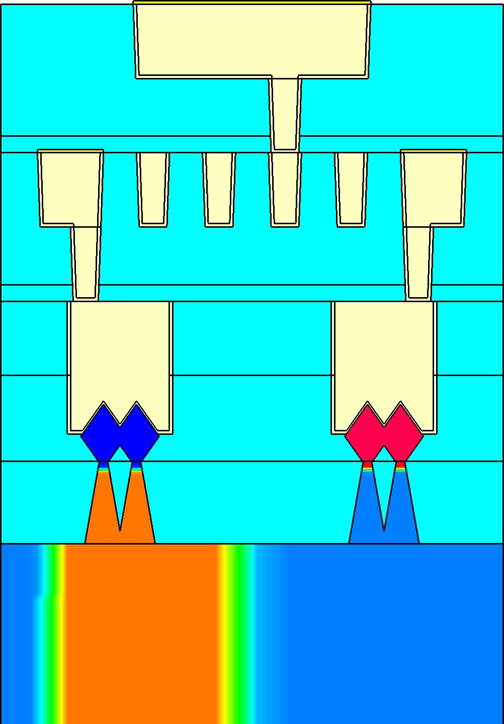
25 Automated parasitics extraction O. Baumgartner et al. (GTS) GTS 20 / 25

26 BEOL resistances & capacitances O. Baumgartner et al. (GTS) GTS 21 / 25

27 FEOL resistances O. Baumgartner et al. (GTS) GTS 22 / 25

28 Multi-scale self-heating O. Baumgartner et al. (GTS) GTS 23 / 25
29 Modules summary Layout-based structrue generation Rapid prototyping Process-flow awareness Device simulation Steady-state, transient, AC Reliability What about calibration? Parasitics extraction R/C-network topology extraction Self-heating Quasi-transient simulation Thermal network extraction O. Baumgartner et al. (GTS) GTS 24 / 25
30 Our solutions Nano-scale TCAD Single-device TCAD Large-scale TCAD Path finding Process to device to cell to circuit variability Design-technology co-optimization (DTCO) O. Baumgartner et al. (GTS) GTS 25 / 25
A Decade of Driving Innovation Physics-based DTCO Full-Cell 3D TCAD. Predictions based on physics.
 A Decade of Driving Innovation Physics-based DTCO Full-Cell 3D TCAD Predictions based on physics. Today's semiconductor industry is facing unprecedented challenges. To survive in highly competitive markets
ENABLEMENT OF COMPACT MODELS FOR
 ENABLEMENT OF COMPACT MODELS FOR ULTRA-SCALED CMOS TECHNOLOGIES D. YAKIMETS, P. SCHUDDINCK, D. JANG, M. GARCIA BARDON, N. SHARAN, B. PARVAIS*, P. RAGHAVAN, AND A. MOCUTA IMEC, KAPELDREEF 75, 3001 LEUVEN,
CHAPTER 5 EFFECT OF GATE ELECTRODE WORK FUNCTION VARIATION ON DC AND AC PARAMETERS IN CONVENTIONAL AND JUNCTIONLESS FINFETS
 98 CHAPTER 5 EFFECT OF GATE ELECTRODE WORK FUNCTION VARIATION ON DC AND AC PARAMETERS IN CONVENTIONAL AND JUNCTIONLESS FINFETS In this chapter, the effect of gate electrode work function variation on DC
Design/Technology Co-Optimisation (DTCO) in the Presence of Acute Variability
 in the Presence of Acute Variability") Design/Technology Co-Optimisation (DTCO) in the Presence of Acute Variability A. Asenov 1,2, E. A. Towie 1!! 1 Gold Standard Simulations Ltd 2 Glasgow University! Summary!! Introduction!! FinFET complexity
Design/Technology Co-Optimisation (DTCO) in the Presence of Acute Variability A. Asenov 1,2, E. A. Towie 1!! 1 Gold Standard Simulations Ltd 2 Glasgow University! Summary!! Introduction!! FinFET complexity
Role of Computer Experiment
 Role of Computer Experiment Experimental World Computer Experiment Theoretical World Accumulation of factual information Checks and stimuli Ordering of factual information into logically coherent patterns
ECE 342 Electronic Circuits. 3. MOS Transistors
 ECE 342 Electronic Circuits 3. MOS Transistors Jose E. Schutt-Aine Electrical & Computer Engineering University of Illinois jschutt@emlab.uiuc.edu 1 NMOS Transistor Typically L = 0.1 to 3 m, W = 0.2 to
Operation and Modeling of. The MOS Transistor. Second Edition. Yannis Tsividis Columbia University. New York Oxford OXFORD UNIVERSITY PRESS
 Operation and Modeling of The MOS Transistor Second Edition Yannis Tsividis Columbia University New York Oxford OXFORD UNIVERSITY PRESS CONTENTS Chapter 1 l.l 1.2 1.3 1.4 1.5 1.6 1.7 Chapter 2 2.1 2.2
The Devices. Digital Integrated Circuits A Design Perspective. Jan M. Rabaey Anantha Chandrakasan Borivoje Nikolic. July 30, 2002
 Digital Integrated Circuits A Design Perspective Jan M. Rabaey Anantha Chandrakasan Borivoje Nikolic The Devices July 30, 2002 Goal of this chapter Present intuitive understanding of device operation Introduction
MOSFET: Introduction
 E&CE 437 Integrated VLSI Systems MOS Transistor 1 of 30 MOSFET: Introduction Metal oxide semiconductor field effect transistor (MOSFET) or MOS is widely used for implementing digital designs Its major
ECE 407 Computer Aided Design for Electronic Systems. Simulation. Instructor: Maria K. Michael. Overview
 407 Computer Aided Design for Electronic Systems Simulation Instructor: Maria K. Michael Overview What is simulation? Design verification Modeling Levels Modeling circuits for simulation True-value simulation
MOS Transistor Properties Review
 MOS Transistor Properties Review 1 VLSI Chip Manufacturing Process Photolithography: transfer of mask patterns to the chip Diffusion or ion implantation: selective doping of Si substrate Oxidation: SiO
ECE 342 Electronic Circuits. Lecture 6 MOS Transistors
 ECE 342 Electronic Circuits Lecture 6 MOS Transistors Jose E. Schutt-Aine Electrical & Computer Engineering University of Illinois jesa@illinois.edu 1 NMOS Transistor Typically L = 0.1 to 3 m, W = 0.2
Digital Integrated Circuits A Design Perspective. Jan M. Rabaey Anantha Chandrakasan Borivoje Nikolic. The Devices. July 30, Devices.
 Digital Integrated Circuits A Design Perspective Jan M. Rabaey Anantha Chandrakasan Borivoje Nikolic The July 30, 2002 1 Goal of this chapter Present intuitive understanding of device operation Introduction
Simple and accurate modeling of the 3D structural variations in FinFETs
 Simple and accurate modeling of the 3D structural variations in FinFETs Donghu Kim Electrical Engineering Program Graduate school of UNIST 2013 Simple and accurate modeling of the 3D structural variations
TCAD Modeling of Stress Impact on Performance and Reliability
 TCAD Modeling of Stress Impact on Performance and Reliability Xiaopeng Xu TCAD R&D, Synopsys March 16, 2010 SEMATECH Workshop on Stress Management for 3D ICs using Through Silicon Vias 1 Outline Introduction
CMOS INVERTER. Last Lecture. Metrics for qualifying digital circuits. »Cost» Reliability» Speed (delay)»performance
»performance") CMOS INVERTER Last Lecture Metrics for qualifying digital circuits»cost» Reliability» Speed (delay)»performance 1 Today s lecture The CMOS inverter at a glance An MOS transistor model for manual analysis
CMOS INVERTER Last Lecture Metrics for qualifying digital circuits»cost» Reliability» Speed (delay)»performance 1 Today s lecture The CMOS inverter at a glance An MOS transistor model for manual analysis
Variability Aware Statistical Timing Modelling Using SPICE Simulations
 Variability Aware Statistical Timing Modelling Using SPICE Simulations Master Thesis by Di Wang Informatics and Mathematical Modelling, Technical University of Denmark January 23, 2008 2 Contents List
Lecture 5: DC & Transient Response
 Lecture 5: DC & Transient Response Outline Pass Transistors DC Response Logic Levels and Noise Margins Transient Response RC Delay Models Delay Estimation 2 Pass Transistors We have assumed source is grounded
Very Large Scale Integration (VLSI)
") Very Large Scale Integration (VLSI) Lecture 4 Dr. Ahmed H. Madian Ah_madian@hotmail.com Dr. Ahmed H. Madian-VLSI Contents Delay estimation Simple RC model Penfield-Rubenstein Model Logical effort Delay
Very Large Scale Integration (VLSI) Lecture 4 Dr. Ahmed H. Madian Ah_madian@hotmail.com Dr. Ahmed H. Madian-VLSI Contents Delay estimation Simple RC model Penfield-Rubenstein Model Logical effort Delay
CMPEN 411 VLSI Digital Circuits. Lecture 03: MOS Transistor
 CMPEN 411 VLSI Digital Circuits Lecture 03: MOS Transistor Kyusun Choi [Adapted from Rabaey s Digital Integrated Circuits, Second Edition, 2003 J. Rabaey, A. Chandrakasan, B. Nikolic] CMPEN 411 L03 S.1
EE115C Digital Electronic Circuits Homework #4
 EE115 Digital Electronic ircuits Homework #4 Problem 1 Power Dissipation Solution Vdd =1.0V onsider the source follower circuit used to drive a load L =20fF shown above. M1 and M2 are both NMOS transistors
EE 330 Lecture 16. MOS Device Modeling p-channel n-channel comparisons Model consistency and relationships CMOS Process Flow
 EE 330 Lecture 16 MOS Device Modeling p-channel n-channel comparisons Model consistency and relationships CMOS Process Flow Review from Last Time Operation Regions by Applications Id I D 300 250 200 150
EE115C Winter 2017 Digital Electronic Circuits. Lecture 3: MOS RC Model, CMOS Manufacturing
 EE115C Winter 2017 Digital Electronic Circuits Lecture 3: MOS RC Model, CMOS Manufacturing Agenda MOS Transistor: RC Model (pp. 104-113) S R on D CMOS Manufacturing Process (pp. 36-46) S S C GS G G C GD
DC and AC modeling of minority carriers currents in ICs substrate
 DC and AC modeling of minority carriers currents in ICs substrate Camillo Stefanucci, Pietro Buccella, Maher Kayal and Jean-Michel Sallese Swiss Federal Institute of Technology Lausanne, Switzerland MOS-AK
DC and Transient. Courtesy of Dr. Daehyun Dr. Dr. Shmuel and Dr.
 DC and Transient Courtesy of Dr. Daehyun Lim@WSU, Dr. Harris@HMC, Dr. Shmuel Wimer@BIU and Dr. Choi@PSU http://csce.uark.edu +1 (479) 575-604 yrpeng@uark.edu Pass Transistors We have assumed source is
Chapter 4 Field-Effect Transistors
 Chapter 4 Field-Effect Transistors Microelectronic Circuit Design Richard C. Jaeger Travis N. Blalock 5/5/11 Chap 4-1 Chapter Goals Describe operation of MOSFETs. Define FET characteristics in operation
Reliability of 3D IC with Via-Middle TSV: Characterization and Modeling
 Reliability of 3D IC with Via-Middle TSV: Characterization and Modeling Victor Moroz *, Munkang Choi *, Geert Van der Plas, Paul Marchal, Kristof Croes, and Eric Beyne * Motivation: Build Reliable 3D IC
VLSI VLSI CIRCUIT DESIGN PROCESSES P.VIDYA SAGAR ( ASSOCIATE PROFESSOR) Department of Electronics and Communication Engineering, VBIT
 Department of Electronics and Communication Engineering, VBIT") VLSI VLSI CIRCUIT DESIGN PROCESSES P.VIDYA SAGAR ( ASSOCIATE PROFESSOR) SYLLABUS UNIT II VLSI CIRCUIT DESIGN PROCESSES: VLSI Design Flow, MOS Layers, Stick Diagrams, Design Rules and Layout, 2 m CMOS Design
VLSI VLSI CIRCUIT DESIGN PROCESSES P.VIDYA SAGAR ( ASSOCIATE PROFESSOR) SYLLABUS UNIT II VLSI CIRCUIT DESIGN PROCESSES: VLSI Design Flow, MOS Layers, Stick Diagrams, Design Rules and Layout, 2 m CMOS Design
VLSI Design, Fall Logical Effort. Jacob Abraham
 6. Logical Effort 6. Logical Effort Jacob Abraham Department of Electrical and Computer Engineering The University of Texas at Austin VLSI Design Fall 207 September 20, 207 ECE Department, University of
Today s lecture. EE141- Spring 2003 Lecture 4. Design Rules CMOS Inverter MOS Transistor Model
 - Spring 003 Lecture 4 Design Rules CMOS Inverter MOS Transistor Model Today s lecture Design Rules The CMOS inverter at a glance An MOS transistor model for manual analysis Important! Labs start next
EECS 312: Digital Integrated Circuits Midterm Exam 2 December 2010
 Signature: EECS 312: Digital Integrated Circuits Midterm Exam 2 December 2010 obert Dick Show your work. Derivations are required for credit; end results are insufficient. Closed book. No electronic mental
Accurate Analysis of the Number of Fins in the Triple- Gate FinFET Capacitance Compact Model
 International Journal of Engineering & Technology IJET-IJENS Vol:15 No:02 1 Accurate Analysis of the Number of Fins in the Triple- Gate FinFET Capacitance Compact Model Omar H. El-Sewefy Mentor Graphics
S No. Questions Bloom s Taxonomy Level UNIT-I
 GROUP-A (SHORT ANSWER QUESTIONS) S No. Questions Bloom s UNIT-I 1 Define oxidation & Classify different types of oxidation Remember 1 2 Explain about Ion implantation Understand 1 3 Describe lithography
CPE/EE 427, CPE 527 VLSI Design I Delay Estimation. Department of Electrical and Computer Engineering University of Alabama in Huntsville
 CPE/EE 47, CPE 57 VLSI Design I Delay Estimation Department of Electrical and Computer Engineering University of labama in Huntsville leksandar Milenkovic ( www.ece.uah.edu/~milenka ) Review: CMOS Circuit
Lecture 5: DC & Transient Response
 Lecture 5: DC & Transient Response Outline q Pass Transistors q DC Response q Logic Levels and Noise Margins q Transient Response q RC Delay Models q Delay Estimation 2 Activity 1) If the width of a transistor
VLSI GATE LEVEL DESIGN UNIT - III P.VIDYA SAGAR ( ASSOCIATE PROFESSOR) Department of Electronics and Communication Engineering, VBIT
 Department of Electronics and Communication Engineering, VBIT") VLSI UNIT - III GATE LEVEL DESIGN P.VIDYA SAGAR ( ASSOCIATE PROFESSOR) contents GATE LEVEL DESIGN : Logic Gates and Other complex gates, Switch logic, Alternate gate circuits, Time Delays, Driving large
VLSI UNIT - III GATE LEVEL DESIGN P.VIDYA SAGAR ( ASSOCIATE PROFESSOR) contents GATE LEVEL DESIGN : Logic Gates and Other complex gates, Switch logic, Alternate gate circuits, Time Delays, Driving large
EECS 312: Digital Integrated Circuits Midterm Exam 2 December 2010
 Signature: EECS 312: Digital Integrated Circuits Midterm Exam 2 December 2010 Robert Dick Show your work. Derivations are required for credit; end results are insufficient. Closed book. No electronic mental
Lecture 6: DC & Transient Response
 Lecture 6: DC & Transient Response Slides courtesy of Deming Chen Slides based on the initial set from David Harris CMOS VLSI Design Outline Pass Transistors DC Response Logic Levels and Noise Margins
L ECE 4211 UConn F. Jain Scaling Laws for NanoFETs Chapter 10 Logic Gate Scaling
 L13 04202017 ECE 4211 UConn F. Jain Scaling Laws for NanoFETs Chapter 10 Logic Gate Scaling Scaling laws: Generalized scaling (GS) p. 610 Design steps p.613 Nanotransistor issues (page 626) Degradation
Modeling Random Variability of 16nm Bulk FinFETs
 Modeling Random Variability of 16nm Bulk FinFETs Victor Moroz, Qiang Lu, and Munkang Choi September 9, 2010 1 Outline 2 Outline 3 16nm Bulk FinFETs for 16nm Node Simulation domain 24nm fin pitch 56nm gate
Fig. 1 CMOS Transistor Circuits (a) Inverter Out = NOT In, (b) NOR-gate C = NOT (A or B)
 Inverter Out = NOT In, (b) NOR-gate C = NOT (A or B)") 1 Introduction to Transistor-Level Logic Circuits 1 By Prawat Nagvajara At the transistor level of logic circuits, transistors operate as switches with the logic variables controlling the open or closed
1 Introduction to Transistor-Level Logic Circuits 1 By Prawat Nagvajara At the transistor level of logic circuits, transistors operate as switches with the logic variables controlling the open or closed
Taurus-Topography. Topography Modeling for IC Technology
 SYSTEMS PRODUCTS LOGICAL PRODUCTS PHYSICAL IMPLEMENTATION SIMULATION AND ANALYSIS LIBRARIES TCAD Aurora DFM WorkBench Davinci Medici Raphael Raphael-NES Silicon Early Access TSUPREM-4 Taurus-Device Taurus-Lithography
Testability. Shaahin Hessabi. Sharif University of Technology. Adapted from the presentation prepared by book authors.
 Testability Lecture 6: Logic Simulation Shaahin Hessabi Department of Computer Engineering Sharif University of Technology Adapted from the presentation prepared by book authors Slide 1 of 27 Outline What
Lecture 12 CMOS Delay & Transient Response
 EE 471: Transport Phenomena in Solid State Devices Spring 2018 Lecture 12 CMOS Delay & Transient Response Bryan Ackland Department of Electrical and Computer Engineering Stevens Institute of Technology
EE5780 Advanced VLSI CAD
 EE5780 Advanced VLSI CAD Lecture 4 DC and Transient Responses, Circuit Delays Zhuo Feng 4.1 Outline Pass Transistors DC Response Logic Levels and Noise Margins Transient Response RC Delay Models Delay
ESE 570: Digital Integrated Circuits and VLSI Fundamentals
 ESE 570: Digital Integrated Circuits and VLSI Fundamentals Lec 4: January 29, 2019 MOS Transistor Theory, MOS Model Penn ESE 570 Spring 2019 Khanna Lecture Outline! CMOS Process Enhancements! Semiconductor
Device Models (PN Diode, MOSFET )
") Device Models (PN Diode, MOSFET ) Instructor: Steven P. Levitan steve@ece.pitt.edu TA: Gayatri Mehta, José Martínez Book: Digital Integrated Circuits: A Design Perspective; Jan Rabaey Lab Notes: Handed
Device Models (PN Diode, MOSFET ) Instructor: Steven P. Levitan steve@ece.pitt.edu TA: Gayatri Mehta, José Martínez Book: Digital Integrated Circuits: A Design Perspective; Jan Rabaey Lab Notes: Handed
EE105 Fall 2014 Microelectronic Devices and Circuits. NMOS Transistor Capacitances: Saturation Region
 EE105 Fall 014 Microelectronic Devices and Circuits Prof. Ming C. Wu wu@eecs.berkeley.edu 511 Sutardja Dai Hall (SDH) 1 NMOS Transistor Capacitances: Saturation Region Drain no longer connected to channel
FLCC Seminar. Spacer Lithography for Reduced Variability in MOSFET Performance
 1 Seminar Spacer Lithography for Reduced Variability in MOSFET Performance Prof. Tsu-Jae King Liu Electrical Engineering & Computer Sciences Dept. University of California at Berkeley Graduate Student:
EE382M-14 CMOS Analog Integrated Circuit Design
 EE382M-14 CMOS Analog Integrated Circuit Design Lecture 3, MOS Capacitances, Passive Components, and Layout of Analog Integrated Circuits MOS Capacitances Type of MOS transistor capacitors Depletion capacitance
Tri-Gate Fully-Depleted CMOS Transistors: Fabrication, Design and Layout
 Tri-Gate Fully-Depleted CMOS Transistors: Fabrication, Design and Layout B.Doyle, J.Kavalieros, T. Linton, R.Rios B.Boyanov, S.Datta, M. Doczy, S.Hareland, B. Jin, R.Chau Logic Technology Development Intel
Digital Integrated Circuits
 Chapter 6 The CMOS Inverter 1 Contents Introduction (MOST models) 0, 1 st, 2 nd order The CMOS inverter : The static behavior: o DC transfer characteristics, o Short-circuit current The CMOS inverter :
CHAPTER 2 AN OVERVIEW OF TCAD SIMULATOR AND SIMULATION METHODOLOGY
 15 CHAPTER 2 AN OVERVIEW OF TCAD SIMULATOR AND SIMULATION METHODOLOGY In this chapter TCAD and the various modules available in the TCAD simulator have been discussed. The simulation methodologies to extract
THE INVERTER. Inverter
 THE INVERTER DIGITAL GATES Fundamental Parameters Functionality Reliability, Robustness Area Performance» Speed (delay)» Power Consumption» Energy Noise in Digital Integrated Circuits v(t) V DD i(t) (a)
Lecture 4: CMOS Transistor Theory
 Introduction to CMOS VLSI Design Lecture 4: CMOS Transistor Theory David Harris, Harvey Mudd College Kartik Mohanram and Steven Levitan University of Pittsburgh Outline q Introduction q MOS Capacitor q
Topic 4. The CMOS Inverter
 Topic 4 The CMOS Inverter Peter Cheung Department of Electrical & Electronic Engineering Imperial College London URL: www.ee.ic.ac.uk/pcheung/ E-mail: p.cheung@ic.ac.uk Topic 4-1 Noise in Digital Integrated
ECE 497 JS Lecture - 12 Device Technologies
 ECE 497 JS Lecture - 12 Device Technologies Spring 2004 Jose E. Schutt-Aine Electrical & Computer Engineering University of Illinois jose@emlab.uiuc.edu 1 NMOS Transistor 2 ρ Source channel charge density
EE 330 Lecture 16. MOSFET Modeling CMOS Process Flow
 EE 330 Lecture 16 MOSFET Modeling CMOS Process Flow Model Extensions 300 Id 250 200 150 100 50 300 0 0 1 2 3 4 5 Vds Existing Model 250 200 Id 150 100 50 Slope is not 0 0 0 1 2 3 4 Actual Device Vds Model
Variability-Aware Compact Model Strategy for 20-nm Bulk MOSFET
 Variability-Aware Compact Model Strategy for 20-nm Bulk MOSFET X. Wang 1, D. Reid 2, L. Wang 1, A. Burenkov 3, C. Millar 2, B. Cheng 2, A. Lange 4, J. Lorenz 3, E. Baer 3, A. Asenov 1,2! 1 Device Modelling
VLSI Design and Simulation
 VLSI Design and Simulation Performance Characterization Topics Performance Characterization Resistance Estimation Capacitance Estimation Inductance Estimation Performance Characterization Inverter Voltage
A Multi-Gate CMOS Compact Model BSIMMG
 A Multi-Gate CMOS Compact Model BSIMMG Darsen Lu, Sriramkumar Venugopalan, Tanvir Morshed, Yogesh Singh Chauhan, Chung-Hsun Lin, Mohan Dunga, Ali Niknejad and Chenming Hu University of California, Berkeley
Practice 3: Semiconductors
 Practice 3: Semiconductors Digital Electronic Circuits Semester A 2012 VLSI Fabrication Process VLSI Very Large Scale Integration The ability to fabricate many devices on a single substrate within a given
MOS Transistor I-V Characteristics and Parasitics
 ECEN454 Digital Integrated Circuit Design MOS Transistor I-V Characteristics and Parasitics ECEN 454 Facts about Transistors So far, we have treated transistors as ideal switches An ON transistor passes
New Material Design and Device Simulation Tool. Dr. Gong Kui HZWTECH
 New Material Design and Device Simulation Tool Dr. Gong Kui HZWTECH 鸿之微科技 ( 上海 ) 股份有限公司 HONGZHIWEI TECHNOLOGY(SHANGHAI) CO.,LTD outline Atomistic-TCAD:new devices simulation tool Applications of Atomistic-TCAD
Chapter 2 Process Variability. Overview. 2.1 Sources and Types of Variations
 Chapter 2 Process Variability Overview Parameter variability has always been an issue in integrated circuits. However, comparing with the size of devices, it is relatively increasing with technology evolution,
Device Models (PN Diode, MOSFET )
") Device Models (PN Diode, MOSFET ) Instructor: Steven P. Levitan steve@ece.pitt.edu TA: Gayatri Mehta, José Martínez Book: Digital Integrated Circuits: A Design Perspective; Jan Rabaey Lab Notes: Handed
Device Models (PN Diode, MOSFET ) Instructor: Steven P. Levitan steve@ece.pitt.edu TA: Gayatri Mehta, José Martínez Book: Digital Integrated Circuits: A Design Perspective; Jan Rabaey Lab Notes: Handed
The Devices. Digital Integrated Circuits A Design Perspective. Jan M. Rabaey Anantha Chandrakasan Borivoje Nikolic. July 30, 2002
 igital Integrated Circuits A esign Perspective Jan M. Rabaey Anantha Chandrakasan Borivoje Nikolic The evices July 30, 2002 Goal of this chapter Present intuitive understanding of device operation Introduction
Lecture 0: Introduction
 Lecture 0: Introduction Introduction q Integrated circuits: many transistors on one chip q Very Large Scale Integration (VLSI): bucketloads! q Complementary Metal Oxide Semiconductor Fast, cheap, low power
EEC 118 Lecture #16: Manufacturability. Rajeevan Amirtharajah University of California, Davis
 EEC 118 Lecture #16: Manufacturability Rajeevan Amirtharajah University of California, Davis Outline Finish interconnect discussion Manufacturability: Rabaey G, H (Kang & Leblebici, 14) Amirtharajah, EEC
NANO-CMOS DESIGN FOR MANUFACTURABILILTY
 NANO-CMOS DESIGN FOR MANUFACTURABILILTY Robust Circuit and Physical Design for Sub-65nm Technology Nodes Ban Wong Franz Zach Victor Moroz An u rag Mittal Greg Starr Andrew Kahng WILEY A JOHN WILEY & SONS,
MOS Transistor Theory
 CHAPTER 3 MOS Transistor Theory Outline 2 1. Introduction 2. Ideal I-V Characteristics 3. Nonideal I-V Effects 4. C-V Characteristics 5. DC Transfer Characteristics 6. Switch-level RC Delay Models MOS
UNIVERSITY OF CALIFORNIA College of Engineering Department of Electrical Engineering and Computer Sciences. Professor Oldham Fall 1999
 UNIVERSITY OF CLIFORNI College of Engineering Department of Electrical Engineering and Computer Sciences Professor Oldham Fall 1999 EECS 40 FINL EXM 13 December 1999 Name: Last, First Student ID: T: Kusuma
P. R. Nelson 1 ECE418 - VLSI. Midterm Exam. Solutions
 P. R. Nelson 1 ECE418 - VLSI Midterm Exam Solutions 1. (8 points) Draw the cross-section view for A-A. The cross-section view is as shown below.. ( points) Can you tell which of the metal1 regions is the
AE74 VLSI DESIGN JUN 2015
 Q.2 a. Write down the different levels of integration of IC industry. (4) b. With neat sketch explain briefly PMOS & NMOS enhancement mode transistor. N-MOS enhancement mode transistor:- This transistor
CMOS logic gates. João Canas Ferreira. March University of Porto Faculty of Engineering
 CMOS logic gates João Canas Ferreira University of Porto Faculty of Engineering March 2016 Topics 1 General structure 2 General properties 3 Cell layout João Canas Ferreira (FEUP) CMOS logic gates March
The Devices: MOS Transistors
 The Devices: MOS Transistors References: Semiconductor Device Fundamentals, R. F. Pierret, Addison-Wesley Digital Integrated Circuits: A Design Perspective, J. Rabaey et.al. Prentice Hall NMOS Transistor
Miscellaneous Lecture topics. Mary Jane Irwin [Adapted from Rabaey s Digital Integrated Circuits, 2002, J. Rabaey et al.]
![Miscellaneous Lecture topics. Mary Jane Irwin [Adapted from Rabaey s Digital Integrated Circuits, 2002, J. Rabaey et al.]](/thumbs/81/84503671.jpg "Miscellaneous Lecture topics. Mary Jane Irwin [Adapted from Rabaey s Digital Integrated Circuits, 2002, J. Rabaey et al.]") Miscellaneous Lecture topics Mary Jane Irwin [dapted from Rabaey s Digital Integrated Circuits, 2002, J. Rabaey et al.] MOS Switches MOS transistors can be viewed as simple switches. In an N-Switch, the
Miscellaneous Lecture topics Mary Jane Irwin [dapted from Rabaey s Digital Integrated Circuits, 2002, J. Rabaey et al.] MOS Switches MOS transistors can be viewed as simple switches. In an N-Switch, the
! CMOS Process Enhancements. ! Semiconductor Physics. " Band gaps. " Field Effects. ! MOS Physics. " Cut-off. " Depletion.
 ESE 570: Digital Integrated Circuits and VLSI Fundamentals Lec 4: January 9, 019 MOS Transistor Theory, MOS Model Lecture Outline CMOS Process Enhancements Semiconductor Physics Band gaps Field Effects
COMP 103. Lecture 10. Inverter Dynamics: The Quest for Performance. Section 5.4.2, What is this lecture+ about? PERFORMANCE
 COMP 103 Lecture 10 Inverter Dynamics: The Quest for Performance Section 5.4.2, 5.4.3 [All lecture notes are adapted from Mary Jane Irwin, Penn State, which were adapted from Rabaey s Digital Integrated
ECE 546 Lecture 10 MOS Transistors
 ECE 546 Lecture 10 MOS Transistors Spring 2018 Jose E. Schutt-Aine Electrical & Computer Engineering University of Illinois jesa@illinois.edu NMOS Transistor NMOS Transistor N-Channel MOSFET Built on p-type
CMPEN 411 VLSI Digital Circuits Spring 2012
 CMPEN 411 VLSI Digital Circuits Spring 2012 Lecture 09: Resistance & Inverter Dynamic View [Adapted from Rabaey s Digital Integrated Circuits, Second Edition, 2003 J. Rabaey, A. Chandrakasan, B. Nikolic]
ECE 438: Digital Integrated Circuits Assignment #4 Solution The Inverter
 ECE 438: Digital Integrated Circuits Assignment #4 The Inverter Text: Chapter 5, Digital Integrated Circuits 2 nd Ed, Rabaey 1) Consider the CMOS inverter circuit in Figure P1 with the following parameters.
9/18/2008 GMU, ECE 680 Physical VLSI Design
 ECE680: Physical VLSI Design Chapter III CMOS Device, Inverter, Combinational circuit Logic and Layout Part 3 Combinational Logic Gates (textbook chapter 6) 9/18/2008 GMU, ECE 680 Physical VLSI Design
Scaling of MOS Circuits. 4. International Technology Roadmap for Semiconductors (ITRS) 6. Scaling factors for device parameters
 6. Scaling factors for device parameters") 1 Scaling of MOS Circuits CONTENTS 1. What is scaling?. Why scaling? 3. Figure(s) of Merit (FoM) for scaling 4. International Technology Roadmap for Semiconductors (ITRS) 5. Scaling models 6. Scaling factors
1 Scaling of MOS Circuits CONTENTS 1. What is scaling?. Why scaling? 3. Figure(s) of Merit (FoM) for scaling 4. International Technology Roadmap for Semiconductors (ITRS) 5. Scaling models 6. Scaling factors
EE 330 Lecture 17. MOSFET Modeling CMOS Process Flow
 EE 330 Lecture 17 MOSFET Modeling CMOS Process Flow Review from Last Lecture Limitations of Existing Models V DD V OUT V OUT V DD?? V IN V OUT V IN V IN V DD Switch-Level Models V DD Simple square-law
MOS Transistor Theory
 MOS Transistor Theory So far, we have viewed a MOS transistor as an ideal switch (digital operation) Reality: less than ideal EE 261 Krish Chakrabarty 1 Introduction So far, we have treated transistors
Lecture 8: Combinational Circuit Design
 Lecture 8: Combinational Circuit Design Mark McDermott Electrical and Computer Engineering The University of Texas at ustin 9/5/8 Verilog to Gates module mux(input s, d0, d, output y); assign y = s? d
ECE321 Electronics I
 ECE31 Electronics Lecture 1: CMOS nverter: Noise Margin & Delay Model Payman Zarkesh-Ha Office: ECE Bldg. 30B Office hours: Tuesday :00-3:00PM or by appointment E-mail: payman@ece.unm.edu Slide: 1 CMOS
Ultimately Scaled CMOS: DG FinFETs?
 Ultimately Scaled CMOS: DG FinFETs? Jerry G. Fossum SOI Group Department of Electrical and Computer Engineering University of Florida Gainesville, FL 32611-6130 J. G. Fossum / 1 Outline Introduction -
CMOS Devices. PN junctions and diodes NMOS and PMOS transistors Resistors Capacitors Inductors Bipolar transistors
 CMOS Devices PN junctions and diodes NMOS and PMOS transistors Resistors Capacitors Inductors Bipolar transistors PN Junctions Diffusion causes depletion region D.R. is insulator and establishes barrier
Lecture 4: DC & Transient Response
 Introduction to CMOS VLSI Design Lecture 4: DC & Transient Response David Harris Harvey Mudd College Spring 004 Outline DC Response Logic Levels and Noise Margins Transient Response Delay Estimation Slide
EE141Microelettronica. CMOS Logic
 Microelettronica CMOS Logic CMOS logic Power consumption in CMOS logic gates Where Does Power Go in CMOS? Dynamic Power Consumption Charging and Discharging Capacitors Short Circuit Currents Short Circuit
5. CMOS Gate Characteristics CS755
 5. CMOS Gate Characteristics Last module: CMOS Transistor theory This module: DC Response Logic Levels and Noise Margins Transient Response Delay Estimation Transistor ehavior 1) If the width of a transistor
ELEN0037 Microelectronic IC Design. Prof. Dr. Michael Kraft
 ELEN0037 Microelectronic IC Design Prof. Dr. Michael Kraft Lecture 2: Technological Aspects Technology Passive components Active components CMOS Process Basic Layout Scaling CMOS Technology Integrated
EE241 - Spring 2000 Advanced Digital Integrated Circuits. Announcements
 EE241 - Spring 2000 Advanced Digital Integrated Circuits Lecture 3 Circuit Optimization for Speed Announcements Tu 2/8/00 class will be pre-taped on Friday, 2/4, 4-5:30 203 McLaughlin Class notes are available
Lecture 34: Portable Systems Technology Background Professor Randy H. Katz Computer Science 252 Fall 1995
 Lecture 34: Portable Systems Technology Background Professor Randy H. Katz Computer Science 252 Fall 1995 RHK.F95 1 Technology Trends: Microprocessor Capacity 100000000 10000000 Pentium Transistors 1000000
Lecture 7 Circuit Delay, Area and Power
 Lecture 7 Circuit Delay, Area and Power lecture notes from S. Mitra Intro VLSI System course (EE271) Introduction to VLSI Systems 1 Circuits and Delay Introduction to VLSI Systems 2 Power, Delay and Area:
Overview of Modeling and Simulation TCAD - FLOOPS / FLOODS
 Overview of Modeling and Simulation TCAD - FLOOPS / FLOODS Modeling Overview Strain Effects Thermal Modeling TCAD Modeling Outline FLOOPS / FLOODS Introduction Progress on GaN Devices Prospects for Reliability
Lecture #39. Transistor Scaling
 Lecture #39 ANNOUNCEMENT Pick up graded HW assignments and exams (78 Cory) Lecture #40 will be the last formal lecture. Class on Friday will be dedicated to a course review (with sample problems). Discussion
Section 12: Intro to Devices
 Section 12: Intro to Devices Extensive reading materials on reserve, including Robert F. Pierret, Semiconductor Device Fundamentals EE143 Ali Javey Bond Model of Electrons and Holes Si Si Si Si Si Si Si