FLCC Seminar. Spacer Lithography for Reduced Variability in MOSFET Performance
|
|
|
- Arnold Arnold
- 6 years ago
- Views:
Transcription

1 1 Seminar Spacer Lithography for Reduced Variability in MOSFET Performance Prof. Tsu-Jae King Liu Electrical Engineering & Computer Sciences Dept. University of California at Berkeley Graduate Student: Ms. Xin Sun
2 2 Introduction Outline MOSFET scaling Lithography challenges Spacer Lithography Device Simulation Study Summary and Future Work

3 3 IC Technology Advancement Improvements in IC performance and cost have been enabled by the steady miniaturization of the transistor Investment Transistor Scaling SMIC s Fab 4 (Beijing, China) Photo by L.R. Huang, DigiTimes Better Performance/Cost 100 International Technology Roadmap for Semiconductors Market Growth PITCH YEAR: HALF-PITCH: 90nm 65nm 45nm 32nm 22nm GATE LENGTH (nm) 10 LOW POWER HIGH PERFORMANCE YEAR

4 4 Metal-Oxide-Semiconductor Field-Effect Transistor: Desired characteristics: High ON current Low OFF current The Bulk-Si MOSFET Source Substrate GATE LENGTH, L g Gate Drain JUNCTION DEPTH, X j OXIDE THICKNESS, Tox M. Bohr, Intel Developer Forum, September 2004 Current flowing between the SOURCE and DRAIN is controlled by the voltage on the GATE electrode N-channel & P-channel MOSFETs operate in a complementary manner CMOS = Complementary MOS CURRENT V T GATE VOLTAGE
5 5 V T Roll-Off M. Okuno et al., 2005 IEDM p. 52 V T decreases with L g Effect is exacerbated by high values of V DS Qualitative explanation: The source & drain p-n junctions assist in depleting the Si underneath the gate. The smaller the L g, the greater the percentage of charge balanced by the S/D p-n junctions: V G n+ n+ x j Large L g : S D p depletion region Small L g : S D
6 6 Sub-Threshold Leakage log I D I ON, low VT I ON, high VT I OFF, low VT S 0 V DD I OFF, high VT V G Leakage current varies exponentially with V T S 60mV/dec at room temperature, due to thermal distribution of carriers within energy bands typically mv/dec for a bulk-si MOSFET
7 7 Parametric Yield smaller L gate High-performance processors TOO SLOW TOO LEAKY are speed-binned Faster chips = more $$$ (These parts have smaller L g ) Leakage is exponentially dependent on V T = f(l g ) Since leakage is now appreciable, parametric yield is being squeezed on both sides Tighter control of L g will be needed with scaling!
8 8 The Sub-Wavelength Gap
9 9 Achieving Sub-Wavelength Resolution 250nm 180nm 90nm and below Design OPC PSM Mask OPC Wafer courtesy M. Rieger (Synopsys, Inc.)

10 10 Geometrical Regularity for Improved Yield Configurable logic block layout A geometrically regular layout should be used to improve the fidelity of printed sub-wavelength features. All MOSFETs are oriented along the same direction Gate lines are placed at regular spacings L. Pillegi et al., 2003 DAC p. 782
 It will eventually be more cost effective to use multiple lower-cost masks to")
11 11 Mask Cost Considerations Mask cost escalates with technology advancement! <λ (minimum half-pitch) It will eventually be more cost effective to use multiple lower-cost masks to define the most critical layer (gate)
12 12 Outline Introduction Spacer Lithography Process flow Application to gate patterning Device Simulation Study Summary and Future Work
13 13 Spacer Lithography Process 1. Deposit & pattern sacrificial layer 2. Deposit mask layer (e.g. Si 3 N 4 ) a-si hard mask (SiO 2 ) poly-si gate layer gate dielectric Si a-si hard mask (SiO 2 ) poly-si gate layer gate dielectric Si 3. Anisotropically etch mask layer spacers a-si hard mask (SiO 2 ) poly-si gate layer gate dielectric 4. Remove sacrificial material; Etch hardmask and poly-si L g,min gates gate dielectric Si Si Note that pitch is 2 that of patterned layer!

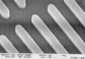
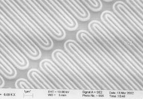
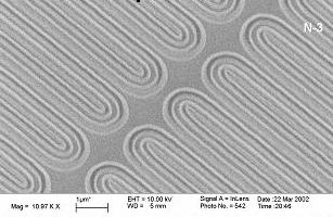
14 14 High-Density Feature Formation Photo-lithographically defined sacrificial structures 1st Spacers 2nd Spacers 3rd Spacers 2 n lines after n iterations of spacer lithography!
15 15 Spacer vs. Resist Lithography Spacer lithography yields superior CD uniformity Y.-K. Choi et al., IEEE Trans. Electron Devices, Vol. 49, p. 436, 2002
16 16 Gate Patterning using Spacer Lithography 1. Define fine-line features in a hard-mask layer using spacer lithography regular geometry (lines and spaces) L g < λ ; pitch P λ 2. Pattern fine-line features (to remove hard-mask where gate lines are not desired) minimum feature size > P alignment tolerance = P L g 3. Define large features in a resist layer using photolithography minimum feature size P alignment tolerance >L g
17 17 Spacer Gate Patterning Benefits Provides fine-line gate electrodes oriented in parallel and laid out on a regular grid Minimizes feature variations for improved yield Facilitates RET to achieve smallest possible feature sizes tight control of L g high parametric yield Note that the geometrically regular mask (Step 1) can be used for multiple chip designs, to save cost
18 18 Achieving Uniform Gate Length L g Gate formation by spacer lithography uniform L g L g Fin formation by conventional lithography non-uniform L g Y.-K. Choi et al., IEDM Technical Digest, pp , 2002
19 19 Outline Introduction Spacer Lithography Device Simulation Study Approach Initial results Summary and Future Work
20 20 Approach Use 3-D device simulations (Sentaurus Device) to investigate the benefits of spacer gate lithography nominal L g < 40nm Sources of variation include: L g variations line-edge roughness (LER) statistical dopant fluctuations (SDF)
 42 40 38 36 34 32 0 200 400 600 800 1000 Line Position")
21 21 EUV Resist LER Data from AMD Average CD = 37.9nm Standard Deviation = 1.7nm Filtered LWR (nm) Line Position (nm)

22 22 Impact of S/D Implant Anneal Conditions RTA: 1000 C 10s Spike: 1100 C 1s Flash: 1300 C 1ms S/D ext. implant: 3E14 As + cm 3keV Trend toward diffusion-less anneal increased junction roughness
23 23 Device Simulation: Methodology LER Generation Structure Generation Device Simulation W channel = 50nm L g = 37nm X j = 20.4nm T ox = 1.2nm N body = 2.2E18cm -3 Assume S/D junction follows LER profile. Sentaurus 3D Device simulation Collect statistical distributions of I ON and I OFF
 Isometric View Plan View (gate electrode) Isometric")
24 24 Simulated MOSFET Structures Resist Lithography Spacer Lithography Plan View (gate electrode) Isometric View Plan View (gate electrode) Isometric View
25 25 Initial Results 0.05 I OFF (ua/um) Conventional Spacer Litho. Smaller spread in I OFF vs. I ON is seen for spacer gate lithography I ON (ma/um)
26 26 Introduction Outline Spacer Lithography Device Simulation Study Summary and Future Work
27 27 Summary Tighter control of L g will be needed with transistor scaling; however, this becomes more difficult as the sub-wavelength gap increases Spacer lithography provides for better CD control, and will eventually be a more cost-effective approach than conventional resist lithography for patterning gate electrodes LER effects on MOSFET performance can be mitigated by spacer gate lithography Future Work Assess the relative impacts of various sources of variability (line-width variations, LER, SDF)
Extending the Era of Moore s Law
 14 nm chip X SEM from www.intel.com/content/dam/www/public/us/en/documents/pdf/foundry/mark bohr 2014 idf presentation.pdf Extending the Era of Moore s Law Tsu Jae King Liu Department of Electrical Engineering
A final review session will be offered on Thursday, May 10 from 10AM to 12noon in 521 Cory (the Hogan Room).
.") A final review session will be offered on Thursday, May 10 from 10AM to 12noon in 521 Cory (the Hogan Room). The Final Exam will take place from 12:30PM to 3:30PM on Saturday May 12 in 60 Evans.» All of
A final review session will be offered on Thursday, May 10 from 10AM to 12noon in 521 Cory (the Hogan Room). The Final Exam will take place from 12:30PM to 3:30PM on Saturday May 12 in 60 Evans.» All of
EE130: Integrated Circuit Devices
 EE130: Integrated Circuit Devices (online at http://webcast.berkeley.edu) Instructor: Prof. Tsu-Jae King (tking@eecs.berkeley.edu) TA s: Marie Eyoum (meyoum@eecs.berkeley.edu) Alvaro Padilla (apadilla@eecs.berkeley.edu)
Lecture #27. The Short Channel Effect (SCE)
") Lecture #27 ANNOUNCEMENTS Design Project: Your BJT design should meet the performance specifications to within 10% at both 300K and 360K. ( β dc > 45, f T > 18 GHz, V A > 9 V and V punchthrough > 9 V )
Lecture #27 ANNOUNCEMENTS Design Project: Your BJT design should meet the performance specifications to within 10% at both 300K and 360K. ( β dc > 45, f T > 18 GHz, V A > 9 V and V punchthrough > 9 V )
Modeling Random Variability of 16nm Bulk FinFETs
 Modeling Random Variability of 16nm Bulk FinFETs Victor Moroz, Qiang Lu, and Munkang Choi September 9, 2010 1 Outline 2 Outline 3 16nm Bulk FinFETs for 16nm Node Simulation domain 24nm fin pitch 56nm gate
Lecture 15 OUTLINE. MOSFET structure & operation (qualitative) Review of electrostatics The (N)MOS capacitor
 Review of electrostatics The (N)MOS capacitor") Lecture 15 OUTLINE MOSFET structure & operation (qualitative) Review of electrostatics The (N)MOS capacitor Electrostatics t ti Charge vs. voltage characteristic Reading: Chapter 6.1 6.2.1 EE105 Fall 2007
Lecture 15 OUTLINE MOSFET structure & operation (qualitative) Review of electrostatics The (N)MOS capacitor Electrostatics t ti Charge vs. voltage characteristic Reading: Chapter 6.1 6.2.1 EE105 Fall 2007
Lecture 15 OUTLINE. MOSFET structure & operation (qualitative) Review of electrostatics The (N)MOS capacitor
 Review of electrostatics The (N)MOS capacitor") Lecture 15 OUTLINE MOSFET structure & operation (qualitative) Review of electrostatics The (N)MOS capacitor Electrostatics Charge vs. voltage characteristic Reading: Chapter 6.1 6.2.1 EE15 Spring 28 Lecture
Lecture 15 OUTLINE MOSFET structure & operation (qualitative) Review of electrostatics The (N)MOS capacitor Electrostatics Charge vs. voltage characteristic Reading: Chapter 6.1 6.2.1 EE15 Spring 28 Lecture
Lecture 0: Introduction
 Lecture 0: Introduction Introduction q Integrated circuits: many transistors on one chip q Very Large Scale Integration (VLSI): bucketloads! q Complementary Metal Oxide Semiconductor Fast, cheap, low power
Chapter 2 Process Variability. Overview. 2.1 Sources and Types of Variations
 Chapter 2 Process Variability Overview Parameter variability has always been an issue in integrated circuits. However, comparing with the size of devices, it is relatively increasing with technology evolution,
Self-study problems and questions Processing and Device Technology, FFF110/FYSD13
 Self-study problems and questions Processing and Device Technology, FFF110/FYSD13 Version 2016_01 In addition to the problems discussed at the seminars and at the lectures, you can use this set of problems
ELEN0037 Microelectronic IC Design. Prof. Dr. Michael Kraft
 ELEN0037 Microelectronic IC Design Prof. Dr. Michael Kraft Lecture 2: Technological Aspects Technology Passive components Active components CMOS Process Basic Layout Scaling CMOS Technology Integrated
Multiple Gate CMOS and Beyond
 Multiple CMOS and Beyond Dept. of EECS, KAIST Yang-Kyu Choi Outline 1. Ultimate Scaling of MOSFETs - 3nm Nanowire FET - 8nm Non-Volatile Memory Device 2. Multiple Functions of MOSFETs 3. Summary 2 CMOS
Tri-Gate Fully-Depleted CMOS Transistors: Fabrication, Design and Layout
 Tri-Gate Fully-Depleted CMOS Transistors: Fabrication, Design and Layout B.Doyle, J.Kavalieros, T. Linton, R.Rios B.Boyanov, S.Datta, M. Doczy, S.Hareland, B. Jin, R.Chau Logic Technology Development Intel
Simple and accurate modeling of the 3D structural variations in FinFETs
 Simple and accurate modeling of the 3D structural variations in FinFETs Donghu Kim Electrical Engineering Program Graduate school of UNIST 2013 Simple and accurate modeling of the 3D structural variations
There s Plenty of Room at the Bottom and at the Top
 14 nm chip X SEM from www.intel.com/content/dam/www/public/us/en/documents/pdf/foundry/mark bohr 2014 idf presentation.pdf There s Plenty of Room at the Bottom and at the Top Tsu Jae King Liu Department
EE143 LAB. Professor N Cheung, U.C. Berkeley
 EE143 LAB 1 1 EE143 Equipment in Cory 218 2 Guidelines for Process Integration * A sequence of Additive and Subtractive steps with lateral patterning Processing Steps Si wafer Watch out for materials compatibility
nmos IC Design Report Module: EEE 112
 nmos IC Design Report Author: 1302509 Zhao Ruimin Module: EEE 112 Lecturer: Date: Dr.Zhao Ce Zhou June/5/2015 Abstract This lab intended to train the experimental skills of the layout designing of the
CHAPTER 5 EFFECT OF GATE ELECTRODE WORK FUNCTION VARIATION ON DC AND AC PARAMETERS IN CONVENTIONAL AND JUNCTIONLESS FINFETS
 98 CHAPTER 5 EFFECT OF GATE ELECTRODE WORK FUNCTION VARIATION ON DC AND AC PARAMETERS IN CONVENTIONAL AND JUNCTIONLESS FINFETS In this chapter, the effect of gate electrode work function variation on DC
Chapter 2. Design and Fabrication of VLSI Devices
 Chapter 2 Design and Fabrication of VLSI Devices Jason Cong 1 Design and Fabrication of VLSI Devices Objectives: To study the materials used in fabrication of VLSI devices. To study the structure of devices
Impact of parametric mismatch and fluctuations on performance and yield of deep-submicron CMOS technologies. Philips Research, The Netherlands
 Impact of parametric mismatch and fluctuations on performance and yield of deep-submicron CMOS technologies Hans Tuinhout, The Netherlands motivation: from deep submicron digital ULSI parametric spread
MOS Transistor Properties Review
 MOS Transistor Properties Review 1 VLSI Chip Manufacturing Process Photolithography: transfer of mask patterns to the chip Diffusion or ion implantation: selective doping of Si substrate Oxidation: SiO
EECS130 Integrated Circuit Devices
 EECS130 Integrated Circuit Devices Professor Ali Javey 10/30/2007 MOSFETs Lecture 4 Reading: Chapter 17, 19 Announcements The next HW set is due on Thursday. Midterm 2 is next week!!!! Threshold and Subthreshold
EE115C Winter 2017 Digital Electronic Circuits. Lecture 3: MOS RC Model, CMOS Manufacturing
 EE115C Winter 2017 Digital Electronic Circuits Lecture 3: MOS RC Model, CMOS Manufacturing Agenda MOS Transistor: RC Model (pp. 104-113) S R on D CMOS Manufacturing Process (pp. 36-46) S S C GS G G C GD
Microelectronics Part 1: Main CMOS circuits design rules
 GBM8320 Dispositifs Médicaux telligents Microelectronics Part 1: Main CMOS circuits design rules Mohamad Sawan et al. Laboratoire de neurotechnologies Polystim! http://www.cours.polymtl.ca/gbm8320/! med-amine.miled@polymtl.ca!
Gold Nanoparticles Floating Gate MISFET for Non-Volatile Memory Applications
 Gold Nanoparticles Floating Gate MISFET for Non-Volatile Memory Applications D. Tsoukalas, S. Kolliopoulou, P. Dimitrakis, P. Normand Institute of Microelectronics, NCSR Demokritos, Athens, Greece S. Paul,
Chapter 3 Basics Semiconductor Devices and Processing
 Chapter 3 Basics Semiconductor Devices and Processing Hong Xiao, Ph. D. www2.austin.cc.tx.us/hongxiao/book.htm Hong Xiao, Ph. D. www2.austin.cc.tx.us/hongxiao/book.htm 1 Objectives Identify at least two
ECE 342 Electronic Circuits. Lecture 6 MOS Transistors
 ECE 342 Electronic Circuits Lecture 6 MOS Transistors Jose E. Schutt-Aine Electrical & Computer Engineering University of Illinois jesa@illinois.edu 1 NMOS Transistor Typically L = 0.1 to 3 m, W = 0.2
Section 12: Intro to Devices
 Section 12: Intro to Devices Extensive reading materials on reserve, including Robert F. Pierret, Semiconductor Device Fundamentals EE143 Ali Javey Bond Model of Electrons and Holes Si Si Si Si Si Si Si
Section 12: Intro to Devices
 Section 12: Intro to Devices Extensive reading materials on reserve, including Robert F. Pierret, Semiconductor Device Fundamentals Bond Model of Electrons and Holes Si Si Si Si Si Si Si Si Si Silicon
ECE 305 Exam 5 SOLUTIONS: Spring 2015 April 17, 2015 Mark Lundstrom Purdue University
 NAME: PUID: : ECE 305 Exam 5 SOLUTIONS: April 17, 2015 Mark Lundstrom Purdue University This is a closed book exam. You may use a calculator and the formula sheet at the end of this exam. Following the
Recent Development of FinFET Technology for CMOS Logic and Memory
 Recent Development of FinFET Technology for CMOS Logic and Memory Chung-Hsun Lin EECS Department University of California at Berkeley Why FinFET Outline FinFET process Unique features of FinFET Mobility,
UNIVERSITY OF CALIFORNIA College of Engineering Department of Electrical Engineering and Computer Sciences. EECS 130 Professor Ali Javey Fall 2006
 UNIVERSITY OF CALIFORNIA College of Engineering Department of Electrical Engineering and Computer Sciences EECS 130 Professor Ali Javey Fall 2006 Midterm 2 Name: SID: Closed book. Two sheets of notes are
EE410 vs. Advanced CMOS Structures
 EE410 vs. Advanced CMOS Structures Prof. Krishna S Department of Electrical Engineering S 1 EE410 CMOS Structure P + poly-si N + poly-si Al/Si alloy LPCVD PSG P + P + N + N + PMOS N-substrate NMOS P-well
MOS Transistors. Prof. Krishna Saraswat. Department of Electrical Engineering Stanford University Stanford, CA
 MOS Transistors Prof. Krishna Saraswat Department of Electrical Engineering S Stanford, CA 94305 saraswat@stanford.edu 1 1930: Patent on the Field-Effect Transistor! Julius Lilienfeld filed a patent describing
MOSFET: Introduction
 E&CE 437 Integrated VLSI Systems MOS Transistor 1 of 30 MOSFET: Introduction Metal oxide semiconductor field effect transistor (MOSFET) or MOS is widely used for implementing digital designs Its major
Chapter 4 Field-Effect Transistors
 Chapter 4 Field-Effect Transistors Microelectronic Circuit Design Richard C. Jaeger Travis N. Blalock 5/5/11 Chap 4-1 Chapter Goals Describe operation of MOSFETs. Define FET characteristics in operation
Make sure the exam paper has 9 pages (including cover page) + 3 pages of data for reference
 + 3 pages of data for reference") UNIVERSITY OF CALIFORNIA College of Engineering Department of Electrical Engineering and Computer Sciences Spring 2006 EE143 Midterm Exam #1 Family Name First name SID Signature Make sure the exam paper
UNIVERSITY OF CALIFORNIA College of Engineering Department of Electrical Engineering and Computer Sciences Spring 2006 EE143 Midterm Exam #1 Family Name First name SID Signature Make sure the exam paper
Future trends in radiation hard electronics
 Future trends in radiation hard electronics F. Faccio CERN, Geneva, Switzerland Outline Radiation effects in CMOS technologies Deep submicron CMOS for radiation environments What is the future going to
P. R. Nelson 1 ECE418 - VLSI. Midterm Exam. Solutions
 P. R. Nelson 1 ECE418 - VLSI Midterm Exam Solutions 1. (8 points) Draw the cross-section view for A-A. The cross-section view is as shown below.. ( points) Can you tell which of the metal1 regions is the
Scaling of MOS Circuits. 4. International Technology Roadmap for Semiconductors (ITRS) 6. Scaling factors for device parameters
 6. Scaling factors for device parameters") 1 Scaling of MOS Circuits CONTENTS 1. What is scaling?. Why scaling? 3. Figure(s) of Merit (FoM) for scaling 4. International Technology Roadmap for Semiconductors (ITRS) 5. Scaling models 6. Scaling factors
1 Scaling of MOS Circuits CONTENTS 1. What is scaling?. Why scaling? 3. Figure(s) of Merit (FoM) for scaling 4. International Technology Roadmap for Semiconductors (ITRS) 5. Scaling models 6. Scaling factors
Extensive reading materials on reserve, including
 Section 12: Intro to Devices Extensive reading materials on reserve, including Robert F. Pierret, Semiconductor Device Fundamentals EE143 Ali Javey Bond Model of Electrons and Holes Si Si Si Si Si Si Si
EE105 Fall 2014 Microelectronic Devices and Circuits. NMOS Transistor Capacitances: Saturation Region
 EE105 Fall 014 Microelectronic Devices and Circuits Prof. Ming C. Wu wu@eecs.berkeley.edu 511 Sutardja Dai Hall (SDH) 1 NMOS Transistor Capacitances: Saturation Region Drain no longer connected to channel
Chapter 5 MOSFET Theory for Submicron Technology
 Chapter 5 MOSFET Theory for Submicron Technology Short channel effects Other small geometry effects Parasitic components Velocity saturation/overshoot Hot carrier effects ** Majority of these notes are
Nanometer Transistors and Their Models. Jan M. Rabaey
 Nanometer Transistors and Their Models Jan M. Rabaey Chapter Outline Nanometer transistor behavior and models Sub-threshold currents and leakage Variability Device and technology innovations Nanometer
Scaling Issues in Planar FET: Dual Gate FET and FinFETs
 Scaling Issues in Planar FET: Dual Gate FET and FinFETs Lecture 12 Dr. Amr Bayoumi Fall 2014 Advanced Devices (EC760) Arab Academy for Science and Technology - Cairo 1 Outline Scaling Issues for Planar
EECS240 Spring Lecture 21: Matching. Elad Alon Dept. of EECS. V i+ V i-
 EECS40 Spring 010 Lecture 1: Matching Elad Alon Dept. of EECS Offset V i+ V i- To achieve zero offset, comparator devices must be perfectly matched to each other How well-matched can the devices be made?
Comparative studies of Ge and Si p-channel metal oxide semiconductor field-effect-transistors with HfSiON dielectric and TaN metal gate
 Comparative studies of Ge and Si p-channel metal oxide semiconductor field-effect-transistors with HfSiON dielectric and TaN metal gate Hu Ai-Bin( 胡爱斌 ) and Xu Qiu-Xia( 徐秋霞 ) Institute of Microelectronics,
Lecture 6 PN Junction and MOS Electrostatics(III) Metal-Oxide-Semiconductor Structure
 Metal-Oxide-Semiconductor Structure") Lecture 6 PN Junction and MOS Electrostatics(III) Metal-Oxide-Semiconductor Structure Outline 1. Introduction to MOS structure 2. Electrostatics of MOS in thermal equilibrium 3. Electrostatics of MOS with
Lecture 6 PN Junction and MOS Electrostatics(III) Metal-Oxide-Semiconductor Structure Outline 1. Introduction to MOS structure 2. Electrostatics of MOS in thermal equilibrium 3. Electrostatics of MOS with
SEMICONDUCTOR MEMORIES
 SEMICONDUCTOR MEMORIES Semiconductor Memory Classification RWM NVRWM ROM Random Access Non-Random Access EPROM E 2 PROM Mask-Programmed Programmable (PROM) SRAM FIFO FLASH DRAM LIFO Shift Register CAM
A Multi-Gate CMOS Compact Model BSIMMG
 A Multi-Gate CMOS Compact Model BSIMMG Darsen Lu, Sriramkumar Venugopalan, Tanvir Morshed, Yogesh Singh Chauhan, Chung-Hsun Lin, Mohan Dunga, Ali Niknejad and Chenming Hu University of California, Berkeley
Circuits. L5: Fabrication and Layout -2 ( ) B. Mazhari Dept. of EE, IIT Kanpur. B. Mazhari, IITK. G-Number
 B. Mazhari Dept. of EE, IIT Kanpur. B. Mazhari, IITK. G-Number") EE610: CMOS Analog Circuits L5: Fabrication and Layout -2 (12.8.2013) B. Mazhari Dept. of EE, IIT Kanpur 44 Passive Components: Resistor Besides MOS transistors, sometimes one requires to implement passive
EE610: CMOS Analog Circuits L5: Fabrication and Layout -2 (12.8.2013) B. Mazhari Dept. of EE, IIT Kanpur 44 Passive Components: Resistor Besides MOS transistors, sometimes one requires to implement passive
A 20 nm gate-length ultra-thin body p-mosfet with silicide source/drain
 Superlattices and Microstructures, Vol. 28, No. 5/6, 2000 doi:10.1006/spmi.2000.0947 Available online at http://www.idealibrary.com on A 20 nm gate-length ultra-thin body p-mosfet with silicide source/drain
Faculty Presentation: Novel Technologies
 2009 IMPACT Workshop Faculty Presentation: Novel Technologies Chenming Hu, EECS Department, UC Berkeley Tsu-Jae King Liu, EECS Department, UC Berkeley Eugene Haller, MS&E Department, UC Berkeley Nathan
Philips Research apple PHILIPS
 c Electronics N.V. 1997 Modelling Compact of Submicron CMOS D.B.M. Klaassen Research Laboratories The Netherlands Eindhoven, contents accuracy and benchmark criteria new applications í RF modelling advanced
Introduction and Background
 Analog CMOS Integrated Circuit Design Introduction and Background Dr. Jawdat Abu-Taha Department of Electrical and Computer Engineering Islamic University of Gaza jtaha@iugaza.edu.ps 1 Marking Assignments
MOS Transistor Theory
 CHAPTER 3 MOS Transistor Theory Outline 2 1. Introduction 2. Ideal I-V Characteristics 3. Nonideal I-V Effects 4. C-V Characteristics 5. DC Transfer Characteristics 6. Switch-level RC Delay Models MOS
The Future of CMOS. David Pulfrey. CHRONOLOGY of the FET. Lecture Lilienfeld s patent (BG FET) 1965 Commercialization (Fairchild)
 1965 Commercialization (Fairchild)") The Future of CMOS David Pulfrey 1 CHRONOLOGY of the FET 1933 Lilienfeld s patent (BG FET) 1965 Commercialization (Fairchild) 1991 The most abundant object made by mankind (C.T. Sah) 2003 The 10 nm FET
The Future of CMOS David Pulfrey 1 CHRONOLOGY of the FET 1933 Lilienfeld s patent (BG FET) 1965 Commercialization (Fairchild) 1991 The most abundant object made by mankind (C.T. Sah) 2003 The 10 nm FET
Lecture 150 Basic IC Processes (10/10/01) Page ECE Analog Integrated Circuits and Systems P.E. Allen
 Page ECE Analog Integrated Circuits and Systems P.E. Allen") Lecture 150 Basic IC Processes (10/10/01) Page 1501 LECTURE 150 BASIC IC PROCESSES (READING: TextSec. 2.2) INTRODUCTION Objective The objective of this presentation is: 1.) Introduce the fabrication of
Lecture 150 Basic IC Processes (10/10/01) Page 1501 LECTURE 150 BASIC IC PROCESSES (READING: TextSec. 2.2) INTRODUCTION Objective The objective of this presentation is: 1.) Introduce the fabrication of
There's Plenty of Room at the Bottom
 There's Plenty of Room at the Bottom 12/29/1959 Feynman asked why not put the entire Encyclopedia Britannica (24 volumes) on a pin head (requires atomic scale recording). He proposed to use electron microscope
An Analytical Model for a Gate-Induced-Drain-Leakage Current in a Buried-Channel PMOSFET
 Journal of the Korean Physical Society, Vol. 4, No. 5, November 00, pp. 86 867 An Analytical Model for a Gate-Induced-Drain-Leakage Current in a Buried-Channel PMOSFET Seong-Ho Kim, Sung-Eun Kim, Joo-Han
Fig The electron mobility for a-si and poly-si TFT.
 Fig. 1-1-1 The electron mobility for a-si and poly-si TFT. Fig. 1-1-2 The aperture ratio for a-si and poly-si TFT. 33 Fig. 1-2-1 All kinds defect well. (a) is the Dirac well. (b) is the repulsive Columbic
Recent Progress and Challenges for Relay Logic Switch Technology
 Recent Progress and Challenges for Relay Logic Switch Technology Tsu-Jae King Liu Louis Hutin, I-Ru Chen, Rhesa Nathanael, Yenhao Chen, Matthew Spencer and Elad Alon Electrical Engineering and Computer
III-V CMOS: What have we learned from HEMTs? J. A. del Alamo, D.-H. Kim 1, T.-W. Kim, D. Jin, and D. A. Antoniadis
 III-V CMOS: What have we learned from HEMTs? J. A. del Alamo, D.-H. Kim 1, T.-W. Kim, D. Jin, and D. A. Antoniadis Microsystems Technology Laboratories, MIT 1 presently with Teledyne Scientific 23rd International
Parallel Processing and Circuit Design with Nano-Electro-Mechanical Relays
 Parallel Processing and Circuit Design with Nano-Electro-Mechanical Relays Elad Alon 1, Tsu-Jae King Liu 1, Vladimir Stojanovic 2, Dejan Markovic 3 1 University of California, Berkeley 2 Massachusetts
SECTION: Circle one: Alam Lundstrom. ECE 305 Exam 5 SOLUTIONS: Spring 2016 April 18, 2016 M. A. Alam and M.S. Lundstrom Purdue University
 NAME: PUID: SECTION: Circle one: Alam Lundstrom ECE 305 Exam 5 SOLUTIONS: April 18, 2016 M A Alam and MS Lundstrom Purdue University This is a closed book exam You may use a calculator and the formula
NANO-CMOS DESIGN FOR MANUFACTURABILILTY
 NANO-CMOS DESIGN FOR MANUFACTURABILILTY Robust Circuit and Physical Design for Sub-65nm Technology Nodes Ban Wong Franz Zach Victor Moroz An u rag Mittal Greg Starr Andrew Kahng WILEY A JOHN WILEY & SONS,
Previously. ESE370: Circuit-Level Modeling, Design, and Optimization for Digital Systems. Today. Variation Types. Fabrication
 ESE370: Circuit-Level Modeling, Design, and Optimization for Digital Systems Previously Understand how to model transistor behavior Given that we know its parameters V dd, V th, t OX, C OX, W, L, N A Day
SINCE MOSFETs are downscaling into nanometer regime,
 3676 IEEE TRANSACTIONS ON ELECTRON DEVICES, VOL. 60, NO. 11, NOVEMBER 013 Investigations on Line-Edge Roughness (LER) and Line-Width Roughness (LWR) in Nanoscale CMOS Technology: Part II Experimental Results
Impact of Scaling on The Effectiveness of Dynamic Power Reduction Schemes
 Impact of Scaling on The Effectiveness of Dynamic Power Reduction Schemes D. Duarte Intel Corporation david.e.duarte@intel.com N. Vijaykrishnan, M.J. Irwin, H-S Kim Department of CSE, Penn State University
Semiconductor Memories
 Semiconductor References: Adapted from: Digital Integrated Circuits: A Design Perspective, J. Rabaey UCB Principles of CMOS VLSI Design: A Systems Perspective, 2nd Ed., N. H. E. Weste and K. Eshraghian
Status. Embedded System Design and Synthesis. Power and temperature Definitions. Acoustic phonons. Optic phonons
 Status http://robertdick.org/esds/ Office: EECS 2417-E Department of Electrical Engineering and Computer Science University of Michigan Specification, languages, and modeling Computational complexity,
Nanoimprint Lithography
 Nanoimprint Lithography Wei Wu Quantum Science Research Advanced Studies HP Labs, Hewlett-Packard Email: wei.wu@hp.com Outline Background Nanoimprint lithography Thermal based UV-based Applications based
Tilted ion implantation as a cost-efficient sublithographic
 Tilted ion implantation as a cost-efficient sublithographic patterning technique Sang Wan Kim 1,a), Peng Zheng 1, Kimihiko Kato 1, Leonard Rubin 2, Tsu-Jae King Liu 1 1 Department of Electrical Engineering
Lecture 11: MOS Transistor
 Lecture 11: MOS Transistor Prof. Niknejad Lecture Outline Review: MOS Capacitors Regions MOS Capacitors (3.8 3.9) CV Curve Threshold Voltage MOS Transistors (4.1 4.3): Overview Cross-section and layout
EE 5211 Analog Integrated Circuit Design. Hua Tang Fall 2012
 EE 5211 Analog Integrated Circuit Design Hua Tang Fall 2012 Today s topic: 1. Introduction to Analog IC 2. IC Manufacturing (Chapter 2) Introduction What is Integrated Circuit (IC) vs discrete circuits?
EE382M-14 CMOS Analog Integrated Circuit Design
 EE382M-14 CMOS Analog Integrated Circuit Design Lecture 3, MOS Capacitances, Passive Components, and Layout of Analog Integrated Circuits MOS Capacitances Type of MOS transistor capacitors Depletion capacitance
DIFFUSION - Chapter 7
 DIFFUSION - Chapter 7 Doping profiles determine many short-channel characteristics in MOS devices. Resistance impacts drive current. Scaling implies all lateral and vertical dimensions scale by the same
Chapter 12: Electrical Properties. RA l
 Charge carriers and conduction: Chapter 12: Electrical Properties Charge carriers include all species capable of transporting electrical charge, including electrons, ions, and electron holes. The latter
The Devices. Digital Integrated Circuits A Design Perspective. Jan M. Rabaey Anantha Chandrakasan Borivoje Nikolic. July 30, 2002
 Digital Integrated Circuits A Design Perspective Jan M. Rabaey Anantha Chandrakasan Borivoje Nikolic The Devices July 30, 2002 Goal of this chapter Present intuitive understanding of device operation Introduction
Feature-level Compensation & Control. Process Integration September 15, A UC Discovery Project
 Feature-level Compensation & Control Process Integration September 15, 2005 A UC Discovery Project Current Milestones Si/Ge-on-insulator and Strained Si-on-insulator Substrate Engineering (M28 YII.13)
Lecture 12: MOS Capacitors, transistors. Context
 Lecture 12: MOS Capacitors, transistors Context In the last lecture, we discussed PN diodes, and the depletion layer into semiconductor surfaces. Small signal models In this lecture, we will apply those
Lecture 12: MOSFET Devices
 Lecture 12: MOSFET Devices Gu-Yeon Wei Division of Engineering and Applied Sciences Harvard University guyeon@eecs.harvard.edu Wei 1 Overview Reading S&S: Chapter 5.1~5.4 Supplemental Reading Background
Ion Implantation. alternative to diffusion for the introduction of dopants essentially a physical process, rather than chemical advantages:
 Ion Implantation alternative to diffusion for the introduction of dopants essentially a physical process, rather than chemical advantages: mass separation allows wide varies of dopants dose control: diffusion
UNIVERSITY OF CALIFORNIA College of Engineering Department of Electrical Engineering and Computer Sciences. Fall Exam 1
 UNIVERSITY OF CALIFORNIA College of Engineering Department of Electrical Engineering and Computer Sciences EECS 143 Fall 2008 Exam 1 Professor Ali Javey Answer Key Name: SID: 1337 Closed book. One sheet
ESE 570: Digital Integrated Circuits and VLSI Fundamentals
 ESE 570: Digital Integrated Circuits and VLSI Fundamentals Lec 4: January 23, 2018 MOS Transistor Theory, MOS Model Penn ESE 570 Spring 2018 Khanna Lecture Outline! CMOS Process Enhancements! Semiconductor
EE 330 Lecture 16. MOS Device Modeling p-channel n-channel comparisons Model consistency and relationships CMOS Process Flow
 EE 330 Lecture 16 MOS Device Modeling p-channel n-channel comparisons Model consistency and relationships CMOS Process Flow Review from Last Time Operation Regions by Applications Id I D 300 250 200 150
Fig. 1 CMOS Transistor Circuits (a) Inverter Out = NOT In, (b) NOR-gate C = NOT (A or B)
 Inverter Out = NOT In, (b) NOR-gate C = NOT (A or B)") 1 Introduction to Transistor-Level Logic Circuits 1 By Prawat Nagvajara At the transistor level of logic circuits, transistors operate as switches with the logic variables controlling the open or closed
1 Introduction to Transistor-Level Logic Circuits 1 By Prawat Nagvajara At the transistor level of logic circuits, transistors operate as switches with the logic variables controlling the open or closed
EE-612: Lecture 22: CMOS Process Steps
 EE-612: Lecture 22: CMOS Process Steps Mark Lundstrom Electrical and Computer Engineering Purdue University West Lafayette, IN USA Fall 2006 NCN www.nanohub.org Lundstrom EE-612 F06 1 outline 1) Unit Process
Molecular Electronics For Fun and Profit(?)
") Molecular Electronics For Fun and Profit(?) Prof. Geoffrey Hutchison Department of Chemistry University of Pittsburgh geoffh@pitt.edu July 22, 2009 http://hutchison.chem.pitt.edu Moore s Law: Transistor
Molecular Electronics For Fun and Profit(?) Prof. Geoffrey Hutchison Department of Chemistry University of Pittsburgh geoffh@pitt.edu July 22, 2009 http://hutchison.chem.pitt.edu Moore s Law: Transistor
ESE 570: Digital Integrated Circuits and VLSI Fundamentals
 ESE 570: Digital Integrated Circuits and VLSI Fundamentals Lec 4: January 29, 2019 MOS Transistor Theory, MOS Model Penn ESE 570 Spring 2019 Khanna Lecture Outline! CMOS Process Enhancements! Semiconductor
ABSTRACT I NTRODUCT ION
 DESIGN OF AN ION IMPLANTATION PROCESS MONITORING CHIP ON I.C.E. AND PROVIDE A METHODOLOGY FOR EVALUATION OF TESTING RESULTS. by JOSEPH J. BURKIS 5th YEAR MiCROELECTRONIC STUDENT ROCHESTER INSTITUTE OF
Lecture 15: Scaling & Economics
 Lecture 15: Scaling & Economics Outline Scaling Transistors Interconnect Future Challenges Economics 2 Moore s Law Recall that Moore s Law has been driving CMOS [Moore65] Corollary: clock speeds have improved
Enhanced Mobility CMOS
 Enhanced Mobility CMOS Judy L. Hoyt I. Åberg, C. Ni Chléirigh, O. Olubuyide, J. Jung, S. Yu, E.A. Fitzgerald, and D.A. Antoniadis Microsystems Technology Laboratory MIT, Cambridge, MA 02139 Acknowledge
an introduction to Semiconductor Devices
 an introduction to Semiconductor Devices Donald A. Neamen Chapter 6 Fundamentals of the Metal-Oxide-Semiconductor Field-Effect Transistor Introduction: Chapter 6 1. MOSFET Structure 2. MOS Capacitor -
Reduction of Self-heating effect in LDMOS devices
 Reduction of Self-heating effect in LDMOS devices T.K.Maiti * and C. K. Maiti ** Department of Electronics and Electrical Communication Engineering, Indian Institute of Technology, Kharagpur-721302, India
EEC 116 Lecture #3: CMOS Inverters MOS Scaling. Rajeevan Amirtharajah University of California, Davis Jeff Parkhurst Intel Corporation
 EEC 116 Lecture #3: CMOS Inverters MOS Scaling Rajeevan Amirtharajah University of California, Davis Jeff Parhurst Intel Corporation Outline Review: Inverter Transfer Characteristics Lecture 3: Noise Margins,
Lecture 25. Semiconductor Memories. Issues in Memory
 Lecture 25 Semiconductor Memories Issues in Memory Memory Classification Memory Architectures TheMemoryCore Periphery 1 Semiconductor Memory Classification RWM NVRWM ROM Random Access Non-Random Access
Digital Integrated Circuits A Design Perspective
 Semiconductor Memories Adapted from Chapter 12 of Digital Integrated Circuits A Design Perspective Jan M. Rabaey et al. Copyright 2003 Prentice Hall/Pearson Outline Memory Classification Memory Architectures
MOSFET SCALING ECE 663
 MOSFET SCALING Scaling of switches Moore s Law economics Moore s Law - #DRAM Bits per chip doubles every 18 months ~5% bigger chips/wafers ~5% design improvements ~50 % Lithography ability to print smaller
MSE 310/ECE 340: Electrical Properties of Materials Fall 2014 Department of Materials Science and Engineering Boise State University
 MSE 310/ECE 340: Electrical Properties of Materials Fall 2014 Department of Materials Science and Engineering Boise State University Practice Final Exam 1 Read the questions carefully Label all figures