ENABLEMENT OF COMPACT MODELS FOR
|
|
|
- Ellen Thomas
- 5 years ago
- Views:
Transcription
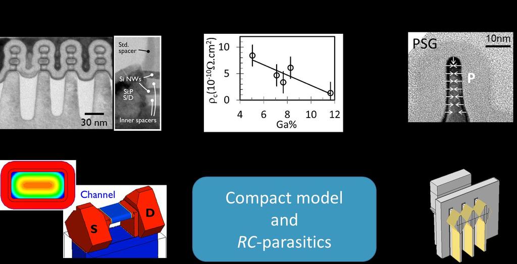
1 ENABLEMENT OF COMPACT MODELS FOR ULTRA-SCALED CMOS TECHNOLOGIES D. YAKIMETS, P. SCHUDDINCK, D. JANG, M. GARCIA BARDON, N. SHARAN, B. PARVAIS*, P. RAGHAVAN, AND A. MOCUTA IMEC, KAPELDREEF 75, 3001 LEUVEN, BELGIUM *ALSO WITH VRIJE UNIVERSITEIT BRUSSEL, BELGIUM 10 TH INTERNATIONAL MOS-AK WORKSHOP DEC. 6, 2017
 Planar device runs out of steam Less happy scaling era Still doubles but device scaling provides diminishing returns 10-7nm: More trouble Multi-patterning cost escalates 14nm: FinFET FinFET device")
2 log 2 (#transistors/$) LOGIC ROADMAP VIEW 20nm: First sign of trouble Double patterning (cost!) Planar device runs out of steam Less happy scaling era Still doubles but device scaling provides diminishing returns 10-7nm: More trouble Multi-patterning cost escalates 14nm: FinFET FinFET device saves the day 28nm 20nm 7-5nm: At last... EUV reduces cost 7nm 10nm 5nm DTCO 14nm Track height reduction Scaling boosters 4-3nm: Nanowire/sheet FET to 2nm: continue gate High-NA length scaling EUV? 2nm 1.5nm 3nm Heterogenous scaling 2D Material for power gating Back Side PDN MRAM. New Compute Machine learning Quantum computing Cryogenic electronics STCO Happy scaling era # transistors per area doubles every two year for same cost 90nm 65nm 40nm Focus of process technology innovation is Scale device and wire Scale basic logic cells Scale (sub-)system functions 2
3 SCALING IS ABOUT POWER-PERFORMANCE-AREA (PPA) AND COST (C) 7nm Node CGP [nm] MP [nm] Cell height Number of fins Area 5nm 7nm T nm T nm 3nm T 2 / Recent scaling trends have involved cell height reduction and fins depopulation causing FEOL structural changes (taller fins / nanosheets) Relative increase in MOL / BEOL importance 3


4 SCALING IS ABOUT POWER-PERFORMANCE-AREA (PPA) AND COST (C) 0.70 V 7nm 5nm 3nm What device architecture / MOL scheme can enable required massive PP gains? 0.65 V -60% -40% Which performance boosters are needed? Stressors Low-k spacers Contact improvements How to enable PPA with compact models? (TCAD is too slow to cover all experiments) 4
5 FLOW FOR PPA ASSESSMENT AT IMEC QUITE COMMON FOR THE INDUSTRY INV layout PEX deck Annotated netlist (cell parasitics + device parameters) PPA RO simulations Parasitics compact model Core compact model (calibrated to TCAD and HW) 5
6 FLOW FOR PPA ASSESSMENT AT IMEC QUITE COMMON FOR THE INDUSTRY INV layout PEX deck Annotated netlist (cell parasitics + device parameters) PPA RO simulations Parasitics compact model Accurate compact models for both intrinsic transport and RC-parasitics are crucial elements of the flow 6 Core compact model (calibrated to TCAD and HW)
7 OUTLINE Introduction Compact model structure: Intrinsic part Parasitics Example of RC-extraction for vertical transistor Summary 7
8 OUTLINE Introduction Compact model structure: Intrinsic part Parasitics Example of RC-extraction for vertical transistor Summary 8
9 HARDWARE-INFLUENCE ON CM DEVELOPMENT EITHER DIRECT ORTHROUGH TCAD 9
10 FLOW FOR PPA ASSESSMENT AT IMEC QUITE COMMON FOR THE INDUSTRY INV layout PEX deck Annotated netlist (cell parasitics + device parameters) PPA RO simulations Parasitics compact model Core compact model (calibrated to TCAD and HW) 10
11 TCAD-BASED COMPACT MODEL FOR INTRINSIC TRANSPORT EXTENDED BSIM-CMG TCAD CM Fitting based on BSIM-CMG model BSIM parameters Ballistic Ratio (Literature or advanced sims) Lg dependence 1. Current (IV) fitting: I DSAT (Lg, Stress) = I BAL (Stress)*BR(L G, Stress) U0 VSAT Ballistic current (TCAD S-band) 1. Full ballistic currents are independent of L G and V D. 2. Quasi-ballistic current by applying BR (L G, Stress) 3. CM is assumed to have no series resistance and ideal electrostatics (Turned off all related BSIM parameters) 2. Capacitance (CV) fitting 1. Capture QM charge centroid behavior 2. Decoupled from IV fitting (QMTCENCV=1) CGS(D)O CGS(D)L QM0 PQM ETAQM TOXP SS DIBL Electrostatics and charge (TCAD DD with QM-corrections) SS/DIBL 3. SS/DIBL fitting CDSC CDSCD DVT1SS CIT ETA0 DSUB DVTP0 DVTP1 11
12 DRIVE CURRENT BALLISTIC CURRENT Full ballistic current provide good indication of intrinsic potential of various devices Si 0.5 Ge 0.5 PFET Si NFET LNW D=7nm FF FinH 30nm, FW 5nm Vdd=0.6V, Ioff = 3.5 na May be easily simulated as a function of stress 12
13 DRIVE CURRENT BALLISTIC CURRENT TIMES BALLISTIC RATIO = TARGET DRIVE CURRENT Ballistic ratio is tricky to compute as various scattering mechanisms affect it Si 0.5 Ge 0.5 PFET Si NFET LNW D=7nm FF FinH 30nm, FW 5nm Vdd=0.6V, Ioff = 3.5 na I DSAT (Lg, Stress) = I BAL (Stress)*BR(L G, Stress) 13
: At low fields μ DD μ low At high fields (high V DS and/or short")
14 HOW TO CAPTURE THIS IN BSIM-CMG? BRIEF THEORETICAL BACKGROUND BSIM model has been described with a drift-diffusion model which is defined by carriers mobility (μ DD ): At low fields μ DD μ low At high fields (high V DS and/or short gates) v sat defines μ DD μ DD (E) = μ low 1 + μ lowe v sat This results in two key parameters: μ low and v sat The μ low is replaced by the apparent mobility due to ballistic mobility reduction and additional scattering mechanisms. 1 = 1 + α μ μ app μ long L G 14
15 CAPACITANCE FITTING BOTH CHANNEL CAPACITANCE AND OVERLAP CAPACITANCE SHOULD BE FITTED FinFET Lg=30nm FW5/FH30 Nanowire Lg=30nm 7nm diameter S-device TCAD results Cgate fitting S-band (no Cov) NanoSheet Lg=30nm 5nm NSH thickness S-device w/ Density gradient TCAD (maker) Fitting results (line) 10, 15, 20nm NSH width Included bias dependency at off-state S-band on long channel ideal device Gate capacitance (channel & S/D overlap) is fitted to S-device TCAD for short-channel devices. 15
16 Drain current (A) HOW TO CAPTURE THIS IN BSIM-CMG? BY MODIFYING CHARGE CENTROID Confinement has been considered in CV fitting by using QMTCENCV=1 but this does not change IV results (i.e. decoupled). 8.E-05 7.E-05 6.E-05 5.E-05 4.E-05 3.E-05 2.E-05 1.E-05 0.E+00 QMTCENCV = 1 QMTCENCV = Gate Voltage (V) <BSIM-CMG v107.0> 16
17 FITTING PROCESS FOR ELECTROSTATICS THE LAST STEP TOWARDS INTRINSIC COMPACT MODEL L G dependency of SS/DIBL at fixed V DD / I OFF (TCAD) <BSIM-CMG v107.0> Tuning BSIM parameters for SS/DIBL separately SPICE simulation at varied L G and same I OFF for single fin structure Comparing between CM and TCAD SS Vt roll-off DIBL Done. In v107.0 BSIM-CMG, Vt roll-off and SS were decoupled by introducing the DVT1SS parameter which simplified fitting a lot. 17
18 ION (ua) SUMMARY ON INTRINSIC TRANSPORT Quasi-Ballistic (S-band + Ballistic ratio) Device model (CM) Electrostatics (S-device) FEOL parasitics imec CM is calibrated with quasi-ballistic current quantum-mechanical CV electrostatics based on TCAD simulation TCAD CM(Quasi-Ballistic) CM(+Electrostatic) LG (nm)
19 OUTLINE Introduction Compact model structure: Intrinsic part Parasitics Example of RC-extraction for vertical transistor Summary 19
20 FLOW FOR PPA ASSESSMENT AT IMEC QUITE COMMON FOR THE INDUSTRY INV layout PEX deck Annotated netlist (cell parasitics + device parameters) PPA RO simulations Parasitics compact model Core compact model (calibrated to TCAD and HW) 20
21 FLOW FOR PPA ASSESSMENT AT IMEC QUITE COMMON FOR THE INDUSTRY INV layout PEX deck Annotated netlist (cell parasitics + device parameters) PPA RO simulations Integration-dependent, hard to maintain in the analytical form even for FF/NW/NSh. Switched to finite element modelling for the RC calculations Parasitics compact model Core compact model (calibrated to TCAD and HW) 21


22 FLOW FOR PPA ASSESSMENT AT IMEC QUITE COMMON FOR THE INDUSTRY Hard to construct for advanced devices (VFET/CFET, etc.) INV layout PEX deck Annotated netlist (cell parasitics + device parameters) PPA Macro-model goes hand-in-hand with device recognition in the PEX deck RO simulations Integration-dependent, hard to maintain in the analytical form even for FF/NW/NSh. Switched to finite element modelling for the RC calculations Parasitics compact model Core compact model (calibrated to TCAD and HW) 22
")
23 POSITION OF THE MACRO MODEL Device model covers parasitic components up to the self-aligned IM1 contact Enforced boundaries result in capacitance loss, say from IM2 to fins (this picture is a bit old, layer names changed, but the idea is correct) 23

24 DISTRIBUTED RC NETWORK COV IS MODELLED IN BSIM Various resistances: Extension S/D Epi Contact M0A core material M0A liners BSIM-CMG Capacitances are computed with 3D finite element modeling software Resistances and capacitances are connected in a distributed network 24
25 EDGE EFFECTS BECOME MORE AND MORE CRITICAL (DUE TO CELL HEIGHT REDUCTION AND FIN DEPOPULATION) Simplified analytic model on relaxed pitches 3D simulations critical at tighter pitches with actual designs from.gds accounting for all fringe capacitances 25

26 ACTUAL DESIGNS FROM.GDS BUT STILL WITH THE SAME DISTINCTION BETWEEN MACRO AND PEX Output is at M1, not captured during 3D RC extraction pmos nmos Independent simulations might be needed if devices are not symmetrical There are a lot of various devices in a full cell library heavy.va look-up tables have to be generated 26

27 FULL TCAD BASED DTCO THAT IS PROBABLY WAY TOO HEAVY Calibrated TCAD deck 27
28 YET, THE IDEA OF RC-EXTRACTION FROM A CELL ISATTRACTIVE (IN THE FORM OF DISTRIBUTED RC-NETLIST) (Almost) no need in a macro model Lighter PEX deck because of simplified device recognition No missing capacitances because there would be no macro / PEX boundary Can this be fast and to be used for full library characterization? As otherwise this solution is limited to the path-finding PPA on RO-level. 28
29 OUTLINE Introduction Compact model structure: Intrinsic part Parasitics Example of RC-extraction for vertical transistor Summary 29
30 AN EXAMPLE OF RC-ANALYSIS OF A VFET DEVICE WHY VERTICAL? --GATE PITCH BUDGETING IS CHALLENGING Spacer Gate Spacer Contact T SP L GATE T SP L SD CGP = Contacted Gate Pitch Parasitic capacitance Reliability Electrostatics control Direct S/D tunneling Gate stack Access resistance S/D stressors 30


31 AN EXAMPLE OF RC-ANALYSIS OF A VFET DEVICE WHY VERTICAL? --GATE PITCH BUDGETING IS CHALLENGING Parasitic capacitance Reliability Electrostatics control Direct S/D tunneling Gate stack Access resistance S/D stressors FinFET Vertical FET 31
32 A VARIANT OF VFET 2-TRANSISTORS PRIMITIVES Vertical devices Common bottom S/D electrode Transistors are chained by pairs This ensures that all device terminals are accessible Physical break in the active no chaining 32
33 A VARIANT OF VFET NAND2 BECOMES THE SMALLEST CELL, NOT INV Series connection is typically tricky with VFETs S/D top1 S/D bot S/D top1 VDD S/D bot S/D top2 VDD Gate Si sheet channel Top Bottom SiGe S/D S/D top2 Z NAND gate structurally reduces by 50% by the absence of dummies VSS 33
34 A VARIANT OF VFET SELF-ALIGNED GATE Gate Top Bottom D NW = 10 nm D D = 20 nm D G S Si VFET D G S D NW = 10 nm D S = 20 nm Si & Si/SiGe VFET Si sheet channel SiGe S/D Make S/D with SiGe instead of Si Possibility to create a thinner core due to different etch rate (Si vs SiGe) 34
![Capacitance [af] Gate Channel KEY CAPACITANCES Electrodes are split into logical segments:](/docs-images/83/87623653/images/35-2.jpg "overlap capacitance capacitance to via.")

35 Capacitance [af] Gate Channel KEY CAPACITANCES Electrodes are split into logical segments: overlap capacitance capacitance to via G-Tov G-Bov G-Top G-Bot G-SiGe Top-Bot Across the fin view G-Bot SiGe G-Tov G-SiGe G-Bov SiGe Dielectrics: HfO 2 SiCO Oxide Conductors: Cobalt Silicon SiGe 35 Along the fin view G-Top SiGe Channel SiGe Top view G-Top Top Top-Bot Bottom
36 SENSITIVITIES TO KEY GEOMETRICAL PARAMETERS CAPS ARE RATHER INSENSITIVE AND DOMINATED BY OVERLAP CAPACITANCE Sensitivities are given around the middle point for every parameter G-Tov G-Bov G-SiGe (bottom) G-Top G-Bot (via) Top-Bop (via) Channel (V G = 0.65 V) 36

37 DEVICE RESISTANCE PLUG IS USED FOR PMOS, BUT NOT FOR NMOS Top contacts 10 nm Plug Top epi nm Bottom epi Bottom contact 37
38 RESISTANCE SENSITIVITIES: TOP THE WIDER THE EXTENSION, ρ THE BETTER THE RESISTANCE R C = C A pmos nmos Holes mobility is smaller than electrons mobility in SiGe pmos nmos ] 38
39 RESISTANCE SENSITIVITIES: BOTTOM CURRENT FLOW IS DIFFERENT FOR NMOS AND PMOS (NAND2 CELL) nmos nmos Contact Contact pmos pmos Plug Plug nmos nmos Contact Contact pmos pmos Plug Plug ] 39
![Active Power [uw] RO PERFORMANCE KEY BOTTLE NECKS MAY BE IDENTIFIED 70 60 50 40 30 20 10 0 2 3 0.90 V 1 4 0.](/docs-images/83/87623653/images/40-1.jpg "55 V 0 20 40 60 80 Frequency [GHz] L G = 15 nm, Bottom SiGe is 25 nm thick, Top SiGe is 10 nm thick Top to bottom via spacing is 7 nm VFET config ρ C [Ωcm 2 ] N SD [cm -3 ] Ext.")
40 Active Power [uw] RO PERFORMANCE KEY BOTTLE NECKS MAY BE IDENTIFIED V V Frequency [GHz] L G = 15 nm, Bottom SiGe is 25 nm thick, Top SiGe is 10 nm thick Top to bottom via spacing is 7 nm VFET config ρ C [Ωcm 2 ] N SD [cm -3 ] Ext. W [nm] Cov [%] 1 1e-9 1e e-10 1e e-10 1e e-10 1e Overlap capacitance limits performance Resistance is less of an issue due to small currents Ext. W 40
41 OUTLINE Introduction Compact model structure: Intrinsic part Parasitics Example of RC-extraction for vertical transistor Summary 41
42 SUMMARY For pre-silicon PPA analysis of advanced nodes, CMs should be very flexible and, ideally, modules based: - stress, - electrostatics, - quasi-ballistic current... Analytical macro-model is hard to maintain as more and more device options appear + various edge effects become non-negligible. Device RC.va look-up tables may be well generated with 3D TCAD tools, but this approach is not sustainable because further library characterization would require exhaustive look-up tables. RC extraction from a full cell might be too time consuming. 42

43
From Physics to Power, Performance, and Parasitics
 From Physics to Power, Performance, and Parasitics The GTS-Team Global TCAD Solutions GmbH, Böserndorferstraße 1/12, 1010 Vienna, Austria O. Baumgartner et al. (GTS) GTS 1 / 25 Scales, methods, hierarchies
MOS Transistor I-V Characteristics and Parasitics
 ECEN454 Digital Integrated Circuit Design MOS Transistor I-V Characteristics and Parasitics ECEN 454 Facts about Transistors So far, we have treated transistors as ideal switches An ON transistor passes
CHAPTER 5 EFFECT OF GATE ELECTRODE WORK FUNCTION VARIATION ON DC AND AC PARAMETERS IN CONVENTIONAL AND JUNCTIONLESS FINFETS
 98 CHAPTER 5 EFFECT OF GATE ELECTRODE WORK FUNCTION VARIATION ON DC AND AC PARAMETERS IN CONVENTIONAL AND JUNCTIONLESS FINFETS In this chapter, the effect of gate electrode work function variation on DC
Design/Technology Co-Optimisation (DTCO) in the Presence of Acute Variability
 in the Presence of Acute Variability") Design/Technology Co-Optimisation (DTCO) in the Presence of Acute Variability A. Asenov 1,2, E. A. Towie 1!! 1 Gold Standard Simulations Ltd 2 Glasgow University! Summary!! Introduction!! FinFET complexity
Design/Technology Co-Optimisation (DTCO) in the Presence of Acute Variability A. Asenov 1,2, E. A. Towie 1!! 1 Gold Standard Simulations Ltd 2 Glasgow University! Summary!! Introduction!! FinFET complexity
Simple and accurate modeling of the 3D structural variations in FinFETs
 Simple and accurate modeling of the 3D structural variations in FinFETs Donghu Kim Electrical Engineering Program Graduate school of UNIST 2013 Simple and accurate modeling of the 3D structural variations
The Critical Role of Quantum Capacitance in Compact Modeling of Nano-Scaled and Nanoelectronic Devices
 The Critical Role of Quantum Capacitance in Compact Modeling of Nano-Scaled and Nanoelectronic Devices Zhiping Yu and Jinyu Zhang Institute of Microelectronics Tsinghua University, Beijing, China yuzhip@tsinghua.edu.cn
CMPEN 411 VLSI Digital Circuits. Lecture 03: MOS Transistor
 CMPEN 411 VLSI Digital Circuits Lecture 03: MOS Transistor Kyusun Choi [Adapted from Rabaey s Digital Integrated Circuits, Second Edition, 2003 J. Rabaey, A. Chandrakasan, B. Nikolic] CMPEN 411 L03 S.1
Lecture 3: CMOS Transistor Theory
 Lecture 3: CMOS Transistor Theory Outline Introduction MOS Capacitor nmos I-V Characteristics pmos I-V Characteristics Gate and Diffusion Capacitance 2 Introduction So far, we have treated transistors
Lecture 4: CMOS Transistor Theory
 Introduction to CMOS VLSI Design Lecture 4: CMOS Transistor Theory David Harris, Harvey Mudd College Kartik Mohanram and Steven Levitan University of Pittsburgh Outline q Introduction q MOS Capacitor q
Device Models (PN Diode, MOSFET )
") Device Models (PN Diode, MOSFET ) Instructor: Steven P. Levitan steve@ece.pitt.edu TA: Gayatri Mehta, José Martínez Book: Digital Integrated Circuits: A Design Perspective; Jan Rabaey Lab Notes: Handed
Device Models (PN Diode, MOSFET ) Instructor: Steven P. Levitan steve@ece.pitt.edu TA: Gayatri Mehta, José Martínez Book: Digital Integrated Circuits: A Design Perspective; Jan Rabaey Lab Notes: Handed
Lecture 5: CMOS Transistor Theory
 Lecture 5: CMOS Transistor Theory Slides courtesy of Deming Chen Slides based on the initial set from David Harris CMOS VLSI Design Outline q q q q q q q Introduction MOS Capacitor nmos I-V Characteristics
EE410 vs. Advanced CMOS Structures
 EE410 vs. Advanced CMOS Structures Prof. Krishna S Department of Electrical Engineering S 1 EE410 CMOS Structure P + poly-si N + poly-si Al/Si alloy LPCVD PSG P + P + N + N + PMOS N-substrate NMOS P-well
Tri-Gate Fully-Depleted CMOS Transistors: Fabrication, Design and Layout
 Tri-Gate Fully-Depleted CMOS Transistors: Fabrication, Design and Layout B.Doyle, J.Kavalieros, T. Linton, R.Rios B.Boyanov, S.Datta, M. Doczy, S.Hareland, B. Jin, R.Chau Logic Technology Development Intel
Enhanced Mobility CMOS
 Enhanced Mobility CMOS Judy L. Hoyt I. Åberg, C. Ni Chléirigh, O. Olubuyide, J. Jung, S. Yu, E.A. Fitzgerald, and D.A. Antoniadis Microsystems Technology Laboratory MIT, Cambridge, MA 02139 Acknowledge
MOSFET: Introduction
 E&CE 437 Integrated VLSI Systems MOS Transistor 1 of 30 MOSFET: Introduction Metal oxide semiconductor field effect transistor (MOSFET) or MOS is widely used for implementing digital designs Its major
Nanoscale CMOS Design Issues
 Nanoscale CMOS Design Issues Jaydeep P. Kulkarni Assistant Professor, ECE Department The University of Texas at Austin jaydeep@austin.utexas.edu Fall, 2017, VLSI-1 Class Transistor I-V Review Agenda Non-ideal
ECE 497 JS Lecture - 12 Device Technologies
 ECE 497 JS Lecture - 12 Device Technologies Spring 2004 Jose E. Schutt-Aine Electrical & Computer Engineering University of Illinois jose@emlab.uiuc.edu 1 NMOS Transistor 2 ρ Source channel charge density
VLSI Design The MOS Transistor
 VLSI Design The MOS Transistor Frank Sill Torres Universidade Federal de Minas Gerais (UFMG), Brazil VLSI Design: CMOS Technology 1 Outline Introduction MOS Capacitor nmos I-V Characteristics pmos I-V
The Devices. Digital Integrated Circuits A Design Perspective. Jan M. Rabaey Anantha Chandrakasan Borivoje Nikolic. July 30, 2002
 Digital Integrated Circuits A Design Perspective Jan M. Rabaey Anantha Chandrakasan Borivoje Nikolic The Devices July 30, 2002 Goal of this chapter Present intuitive understanding of device operation Introduction
Device Models (PN Diode, MOSFET )
") Device Models (PN Diode, MOSFET ) Instructor: Steven P. Levitan steve@ece.pitt.edu TA: Gayatri Mehta, José Martínez Book: Digital Integrated Circuits: A Design Perspective; Jan Rabaey Lab Notes: Handed
Device Models (PN Diode, MOSFET ) Instructor: Steven P. Levitan steve@ece.pitt.edu TA: Gayatri Mehta, José Martínez Book: Digital Integrated Circuits: A Design Perspective; Jan Rabaey Lab Notes: Handed
A Multi-Gate CMOS Compact Model BSIMMG
 A Multi-Gate CMOS Compact Model BSIMMG Darsen Lu, Sriramkumar Venugopalan, Tanvir Morshed, Yogesh Singh Chauhan, Chung-Hsun Lin, Mohan Dunga, Ali Niknejad and Chenming Hu University of California, Berkeley
III-V CMOS: What have we learned from HEMTs? J. A. del Alamo, D.-H. Kim 1, T.-W. Kim, D. Jin, and D. A. Antoniadis
 III-V CMOS: What have we learned from HEMTs? J. A. del Alamo, D.-H. Kim 1, T.-W. Kim, D. Jin, and D. A. Antoniadis Microsystems Technology Laboratories, MIT 1 presently with Teledyne Scientific 23rd International
ELEN0037 Microelectronic IC Design. Prof. Dr. Michael Kraft
 ELEN0037 Microelectronic IC Design Prof. Dr. Michael Kraft Lecture 2: Technological Aspects Technology Passive components Active components CMOS Process Basic Layout Scaling CMOS Technology Integrated
MOS Transistor Theory
 CHAPTER 3 MOS Transistor Theory Outline 2 1. Introduction 2. Ideal I-V Characteristics 3. Nonideal I-V Effects 4. C-V Characteristics 5. DC Transfer Characteristics 6. Switch-level RC Delay Models MOS
The Devices: MOS Transistors
 The Devices: MOS Transistors References: Semiconductor Device Fundamentals, R. F. Pierret, Addison-Wesley Digital Integrated Circuits: A Design Perspective, J. Rabaey et.al. Prentice Hall NMOS Transistor
ENEE 359a Digital VLSI Design
 SLIDE 1 ENEE 359a Digital VLSI Design & Logical Effort Prof. blj@ece.umd.edu Credit where credit is due: Slides contain original artwork ( Jacob 2004) as well as material taken liberally from Irwin & Vijay
Prospects for Ge MOSFETs
 Prospects for Ge MOSFETs Sematech Workshop December 4, 2005 Dimitri A. Antoniadis Microsystems Technology Laboratories MIT Sematech Workshop 2005 1 Channel Transport - I D I D =WQ i (x 0 )v xo v xo : carrier
ECE 342 Electronic Circuits. 3. MOS Transistors
 ECE 342 Electronic Circuits 3. MOS Transistors Jose E. Schutt-Aine Electrical & Computer Engineering University of Illinois jschutt@emlab.uiuc.edu 1 NMOS Transistor Typically L = 0.1 to 3 m, W = 0.2 to
SELECTIVE ETCH REQUIREMENTS FOR THE NEXT GENERATION OF SEMICONDUCTOR DEVICES
 SELECTIVE ETCH REQUIREMENTS FOR THE NEXT GENERATION OF SEMICONDUCTOR DEVICES FRANK HOLSTEYNS ON BEHALF OF THE SURFACE AND INTERFACE PREPARATION GROUP OF THE UNIT PROCESS DEPARTMENT 10 TH OF APRIL 2018
MOS Transistor Theory
 MOS Transistor Theory So far, we have viewed a MOS transistor as an ideal switch (digital operation) Reality: less than ideal EE 261 Krish Chakrabarty 1 Introduction So far, we have treated transistors
Thin Film Transistors (TFT)
") Thin Film Transistors (TFT) a-si TFT - α-si:h (Hydrogenated amorphous Si) deposited with a PECVD system (low temp. process) replaces the single crystal Si substrate. - Inverted staggered structure with
Thin Film Transistors (TFT) a-si TFT - α-si:h (Hydrogenated amorphous Si) deposited with a PECVD system (low temp. process) replaces the single crystal Si substrate. - Inverted staggered structure with
Scaling Issues in Planar FET: Dual Gate FET and FinFETs
 Scaling Issues in Planar FET: Dual Gate FET and FinFETs Lecture 12 Dr. Amr Bayoumi Fall 2014 Advanced Devices (EC760) Arab Academy for Science and Technology - Cairo 1 Outline Scaling Issues for Planar
EE5311- Digital IC Design
 EE5311- Digital IC Design Module 1 - The Transistor Janakiraman V Assistant Professor Department of Electrical Engineering Indian Institute of Technology Madras Chennai October 28, 2017 Janakiraman, IITM
Digital Integrated Circuits A Design Perspective. Jan M. Rabaey Anantha Chandrakasan Borivoje Nikolic. The Devices. July 30, Devices.
 Digital Integrated Circuits A Design Perspective Jan M. Rabaey Anantha Chandrakasan Borivoje Nikolic The July 30, 2002 1 Goal of this chapter Present intuitive understanding of device operation Introduction
ECE 546 Lecture 10 MOS Transistors
 ECE 546 Lecture 10 MOS Transistors Spring 2018 Jose E. Schutt-Aine Electrical & Computer Engineering University of Illinois jesa@illinois.edu NMOS Transistor NMOS Transistor N-Channel MOSFET Built on p-type
Lecture 12: MOS Capacitors, transistors. Context
 Lecture 12: MOS Capacitors, transistors Context In the last lecture, we discussed PN diodes, and the depletion layer into semiconductor surfaces. Small signal models In this lecture, we will apply those
Multiple Gate CMOS and Beyond
 Multiple CMOS and Beyond Dept. of EECS, KAIST Yang-Kyu Choi Outline 1. Ultimate Scaling of MOSFETs - 3nm Nanowire FET - 8nm Non-Volatile Memory Device 2. Multiple Functions of MOSFETs 3. Summary 2 CMOS
CMOS Technology for Computer Architects
 CMOS Technology for Computer Architects Recap Technology Trends Lecture 2: Transistor Inverter Iakovos Mavroidis Giorgos Passas Manolis Katevenis FORTH-ICS (University of Crete) 1 2 Recap Threshold Voltage
The Devices. Devices
 The The MOS Transistor Gate Oxyde Gate Source n+ Polysilicon Drain n+ Field-Oxyde (SiO 2 ) p-substrate p+ stopper Bulk Contact CROSS-SECTION of NMOS Transistor Cross-Section of CMOS Technology MOS transistors
Fig. 1 CMOS Transistor Circuits (a) Inverter Out = NOT In, (b) NOR-gate C = NOT (A or B)
 Inverter Out = NOT In, (b) NOR-gate C = NOT (A or B)") 1 Introduction to Transistor-Level Logic Circuits 1 By Prawat Nagvajara At the transistor level of logic circuits, transistors operate as switches with the logic variables controlling the open or closed
1 Introduction to Transistor-Level Logic Circuits 1 By Prawat Nagvajara At the transistor level of logic circuits, transistors operate as switches with the logic variables controlling the open or closed
TCAD Modeling of Stress Impact on Performance and Reliability
 TCAD Modeling of Stress Impact on Performance and Reliability Xiaopeng Xu TCAD R&D, Synopsys March 16, 2010 SEMATECH Workshop on Stress Management for 3D ICs using Through Silicon Vias 1 Outline Introduction
Section 12: Intro to Devices
 Section 12: Intro to Devices Extensive reading materials on reserve, including Robert F. Pierret, Semiconductor Device Fundamentals EE143 Ali Javey Bond Model of Electrons and Holes Si Si Si Si Si Si Si
Chapter 2 CMOS Transistor Theory. Jin-Fu Li Department of Electrical Engineering National Central University Jungli, Taiwan
 Chapter 2 CMOS Transistor Theory Jin-Fu Li Department of Electrical Engineering National Central University Jungli, Taiwan Outline Introduction MOS Device Design Equation Pass Transistor Jin-Fu Li, EE,
ESE 570: Digital Integrated Circuits and VLSI Fundamentals
 ESE 570: Digital Integrated Circuits and VLSI Fundamentals Lec 4: January 29, 2019 MOS Transistor Theory, MOS Model Penn ESE 570 Spring 2019 Khanna Lecture Outline! CMOS Process Enhancements! Semiconductor
This is the author s final accepted version.
 Al-Ameri, T., Georgiev, V.P., Adamu-Lema, F. and Asenov, A. (2017) Does a Nanowire Transistor Follow the Golden Ratio? A 2D Poisson- Schrödinger/3D Monte Carlo Simulation Study. In: 2017 International
Lecture 11: MOSFET Modeling
 Digital Integrated Circuits (83-313) Lecture 11: MOSFET ing Semester B, 2016-17 Lecturer: Dr. Adam Teman TAs: Itamar Levi, Robert Giterman 18 June 2017 Disclaimer: This course was prepared, in its entirety,
ESE 570: Digital Integrated Circuits and VLSI Fundamentals
 ESE 570: Digital Integrated Circuits and VLSI Fundamentals Lec 4: January 23, 2018 MOS Transistor Theory, MOS Model Penn ESE 570 Spring 2018 Khanna Lecture Outline! CMOS Process Enhancements! Semiconductor
Lecture #27. The Short Channel Effect (SCE)
") Lecture #27 ANNOUNCEMENTS Design Project: Your BJT design should meet the performance specifications to within 10% at both 300K and 360K. ( β dc > 45, f T > 18 GHz, V A > 9 V and V punchthrough > 9 V )
Lecture #27 ANNOUNCEMENTS Design Project: Your BJT design should meet the performance specifications to within 10% at both 300K and 360K. ( β dc > 45, f T > 18 GHz, V A > 9 V and V punchthrough > 9 V )
Spiral 2 7. Capacitance, Delay and Sizing. Mark Redekopp
 2-7.1 Spiral 2 7 Capacitance, Delay and Sizing Mark Redekopp 2-7.2 Learning Outcomes I understand the sources of capacitance in CMOS circuits I understand how delay scales with resistance, capacitance
FLCC Seminar. Spacer Lithography for Reduced Variability in MOSFET Performance
 1 Seminar Spacer Lithography for Reduced Variability in MOSFET Performance Prof. Tsu-Jae King Liu Electrical Engineering & Computer Sciences Dept. University of California at Berkeley Graduate Student:
L ECE 4211 UConn F. Jain Scaling Laws for NanoFETs Chapter 10 Logic Gate Scaling
 L13 04202017 ECE 4211 UConn F. Jain Scaling Laws for NanoFETs Chapter 10 Logic Gate Scaling Scaling laws: Generalized scaling (GS) p. 610 Design steps p.613 Nanotransistor issues (page 626) Degradation
EECS130 Integrated Circuit Devices
 EECS130 Integrated Circuit Devices Professor Ali Javey 10/30/2007 MOSFETs Lecture 4 Reading: Chapter 17, 19 Announcements The next HW set is due on Thursday. Midterm 2 is next week!!!! Threshold and Subthreshold
EECS240 Spring Today s Lecture. Lecture 2: CMOS Technology and Passive Devices. Lingkai Kong EECS. EE240 CMOS Technology
 EECS240 Spring 2013 Lecture 2: CMOS Technology and Passive Devices Lingkai Kong EECS Today s Lecture EE240 CMOS Technology Passive devices Motivation Resistors Capacitors (Inductors) Next time: MOS transistor
Testability. Shaahin Hessabi. Sharif University of Technology. Adapted from the presentation prepared by book authors.
 Testability Lecture 6: Logic Simulation Shaahin Hessabi Department of Computer Engineering Sharif University of Technology Adapted from the presentation prepared by book authors Slide 1 of 27 Outline What
VLSI GATE LEVEL DESIGN UNIT - III P.VIDYA SAGAR ( ASSOCIATE PROFESSOR) Department of Electronics and Communication Engineering, VBIT
 Department of Electronics and Communication Engineering, VBIT") VLSI UNIT - III GATE LEVEL DESIGN P.VIDYA SAGAR ( ASSOCIATE PROFESSOR) contents GATE LEVEL DESIGN : Logic Gates and Other complex gates, Switch logic, Alternate gate circuits, Time Delays, Driving large
VLSI UNIT - III GATE LEVEL DESIGN P.VIDYA SAGAR ( ASSOCIATE PROFESSOR) contents GATE LEVEL DESIGN : Logic Gates and Other complex gates, Switch logic, Alternate gate circuits, Time Delays, Driving large
ECE 342 Electronic Circuits. Lecture 6 MOS Transistors
 ECE 342 Electronic Circuits Lecture 6 MOS Transistors Jose E. Schutt-Aine Electrical & Computer Engineering University of Illinois jesa@illinois.edu 1 NMOS Transistor Typically L = 0.1 to 3 m, W = 0.2
EE115C Winter 2017 Digital Electronic Circuits. Lecture 3: MOS RC Model, CMOS Manufacturing
 EE115C Winter 2017 Digital Electronic Circuits Lecture 3: MOS RC Model, CMOS Manufacturing Agenda MOS Transistor: RC Model (pp. 104-113) S R on D CMOS Manufacturing Process (pp. 36-46) S S C GS G G C GD
A final review session will be offered on Thursday, May 10 from 10AM to 12noon in 521 Cory (the Hogan Room).
.") A final review session will be offered on Thursday, May 10 from 10AM to 12noon in 521 Cory (the Hogan Room). The Final Exam will take place from 12:30PM to 3:30PM on Saturday May 12 in 60 Evans.» All of
A final review session will be offered on Thursday, May 10 from 10AM to 12noon in 521 Cory (the Hogan Room). The Final Exam will take place from 12:30PM to 3:30PM on Saturday May 12 in 60 Evans.» All of
HW 5 posted due in two weeks Lab this week Midterm graded Project to be launched in week 7
 HW 5 posted due in two weeks Lab this week Midterm graded Project to be launched in week 7 2 What do digital IC designers need to know? 5 EE4 EECS4 6 3 0< V GS - V T < V DS Pinch-off 7 For (V GS V T )
Low Contact Resistance on p-sige Junctions with B / Ga Implants and Nanosecond Laser Anneal
 Low Contact Resistance on p-sige Junctions with B / Ga Implants and Nanosecond Laser Anneal Fareen Adeni Khaja Technical Product Marketing, Front End Products Transistor and Interconnect Group Applied
EE105 - Fall 2006 Microelectronic Devices and Circuits
 EE105 - Fall 2006 Microelectronic Devices and Circuits Prof. Jan M. Rabaey (jan@eecs) Lecture 7: MOS Transistor Some Administrative Issues Lab 2 this week Hw 2 due on We Hw 3 will be posted same day MIDTERM
The Future of CMOS. David Pulfrey. CHRONOLOGY of the FET. Lecture Lilienfeld s patent (BG FET) 1965 Commercialization (Fairchild)
 1965 Commercialization (Fairchild)") The Future of CMOS David Pulfrey 1 CHRONOLOGY of the FET 1933 Lilienfeld s patent (BG FET) 1965 Commercialization (Fairchild) 1991 The most abundant object made by mankind (C.T. Sah) 2003 The 10 nm FET
The Future of CMOS David Pulfrey 1 CHRONOLOGY of the FET 1933 Lilienfeld s patent (BG FET) 1965 Commercialization (Fairchild) 1991 The most abundant object made by mankind (C.T. Sah) 2003 The 10 nm FET
CMOS Devices. PN junctions and diodes NMOS and PMOS transistors Resistors Capacitors Inductors Bipolar transistors
 CMOS Devices PN junctions and diodes NMOS and PMOS transistors Resistors Capacitors Inductors Bipolar transistors PN Junctions Diffusion causes depletion region D.R. is insulator and establishes barrier
! CMOS Process Enhancements. ! Semiconductor Physics. " Band gaps. " Field Effects. ! MOS Physics. " Cut-off. " Depletion.
 ESE 570: Digital Integrated Circuits and VLSI Fundamentals Lec 4: January 9, 019 MOS Transistor Theory, MOS Model Lecture Outline CMOS Process Enhancements Semiconductor Physics Band gaps Field Effects
BSIM-CMG Model. Berkeley Common-Gate Multi-Gate MOSFET Model
 BSIM-CMG Model Why BSIM-CMG Model When we reach the end of the technology roadmap for the classical CMOS, multigate (MG) CMOS structures will likely take up the baton. Numerous efforts are underway to
A Verilog-A Compact Model for Negative Capacitance FET
 A Verilog-A Compact Model for Negative Capacitance FET Version.. Muhammad Abdul Wahab and Muhammad Ashraful Alam Purdue University West Lafayette, IN 4797 Last Updated: Oct 2, 25 Table of Contents. Introduction...
LAYOUT TECHNIQUES. Dr. Ivan Grech
 LAYOUT TECHNIQUES OUTLINE Transistor Layout Resistor Layout Capacitor Layout Floor planning Mixed A/D Layout Automatic Analog Layout Layout Techniques Main Layers in a typical Double-Poly, Double-Metal
EE105 - Fall 2005 Microelectronic Devices and Circuits
 EE105 - Fall 005 Microelectronic Devices and Circuits ecture 7 MOS Transistor Announcements Homework 3, due today Homework 4 due next week ab this week Reading: Chapter 4 1 ecture Material ast lecture
Lecture 7 Circuit Delay, Area and Power
 Lecture 7 Circuit Delay, Area and Power lecture notes from S. Mitra Intro VLSI System course (EE271) Introduction to VLSI Systems 1 Circuits and Delay Introduction to VLSI Systems 2 Power, Delay and Area:
Lecture 5: DC & Transient Response
 Lecture 5: DC & Transient Response Outline q Pass Transistors q DC Response q Logic Levels and Noise Margins q Transient Response q RC Delay Models q Delay Estimation 2 Activity 1) If the width of a transistor
Ultimately Scaled CMOS: DG FinFETs?
 Ultimately Scaled CMOS: DG FinFETs? Jerry G. Fossum SOI Group Department of Electrical and Computer Engineering University of Florida Gainesville, FL 32611-6130 J. G. Fossum / 1 Outline Introduction -
Lecture 6 Power Zhuo Feng. Z. Feng MTU EE4800 CMOS Digital IC Design & Analysis 2010
 EE4800 CMOS Digital IC Design & Analysis Lecture 6 Power Zhuo Feng 6.1 Outline Power and Energy Dynamic Power Static Power 6.2 Power and Energy Power is drawn from a voltage source attached to the V DD
Lecture 11: MOS Transistor
 Lecture 11: MOS Transistor Prof. Niknejad Lecture Outline Review: MOS Capacitors Regions MOS Capacitors (3.8 3.9) CV Curve Threshold Voltage MOS Transistors (4.1 4.3): Overview Cross-section and layout
Modeling Random Variability of 16nm Bulk FinFETs
 Modeling Random Variability of 16nm Bulk FinFETs Victor Moroz, Qiang Lu, and Munkang Choi September 9, 2010 1 Outline 2 Outline 3 16nm Bulk FinFETs for 16nm Node Simulation domain 24nm fin pitch 56nm gate
CARNEGIE MELLON UNIVERSITY DEPARTMENT OF ELECTRICAL AND COMPUTER ENGINEERING DIGITAL INTEGRATED CIRCUITS FALL 2002
 CARNEGIE MELLON UNIVERSITY DEPARTMENT OF ELECTRICAL AND COMPUTER ENGINEERING 18-322 DIGITAL INTEGRATED CIRCUITS FALL 2002 Final Examination, Monday Dec. 16, 2002 NAME: SECTION: Time: 180 minutes Closed
Chapter 4 Field-Effect Transistors
 Chapter 4 Field-Effect Transistors Microelectronic Circuit Design Richard C. Jaeger Travis N. Blalock 5/5/11 Chap 4-1 Chapter Goals Describe operation of MOSFETs. Define FET characteristics in operation
EE5780 Advanced VLSI CAD
 EE5780 Advanced VLSI CAD Lecture 4 DC and Transient Responses, Circuit Delays Zhuo Feng 4.1 Outline Pass Transistors DC Response Logic Levels and Noise Margins Transient Response RC Delay Models Delay
Components Research, TMG Intel Corporation *QinetiQ. Contact:
 1 High-Performance 4nm Gate Length InSb P-Channel Compressively Strained Quantum Well Field Effect Transistors for Low-Power (V CC =.5V) Logic Applications M. Radosavljevic,, T. Ashley*, A. Andreev*, S.
Extensive reading materials on reserve, including
 Section 12: Intro to Devices Extensive reading materials on reserve, including Robert F. Pierret, Semiconductor Device Fundamentals EE143 Ali Javey Bond Model of Electrons and Holes Si Si Si Si Si Si Si
Carbon Nanotube Electronics
 Carbon Nanotube Electronics Jeorg Appenzeller, Phaedon Avouris, Vincent Derycke, Stefan Heinz, Richard Martel, Marko Radosavljevic, Jerry Tersoff, Shalom Wind H.-S. Philip Wong hspwong@us.ibm.com IBM T.J.
Scaling of MOS Circuits. 4. International Technology Roadmap for Semiconductors (ITRS) 6. Scaling factors for device parameters
 6. Scaling factors for device parameters") 1 Scaling of MOS Circuits CONTENTS 1. What is scaling?. Why scaling? 3. Figure(s) of Merit (FoM) for scaling 4. International Technology Roadmap for Semiconductors (ITRS) 5. Scaling models 6. Scaling factors
1 Scaling of MOS Circuits CONTENTS 1. What is scaling?. Why scaling? 3. Figure(s) of Merit (FoM) for scaling 4. International Technology Roadmap for Semiconductors (ITRS) 5. Scaling models 6. Scaling factors
Section 12: Intro to Devices
 Section 12: Intro to Devices Extensive reading materials on reserve, including Robert F. Pierret, Semiconductor Device Fundamentals Bond Model of Electrons and Holes Si Si Si Si Si Si Si Si Si Silicon
ESE 570: Digital Integrated Circuits and VLSI Fundamentals
 ESE 570: Digital Integrated Circuits and VLSI Fundamentals Lec 15: March 15, 2018 Euler Paths, Energy Basics and Optimization Midterm! Midterm " Mean: 89.7 " Standard Dev: 8.12 2 Lecture Outline! Euler
EE 466/586 VLSI Design. Partha Pande School of EECS Washington State University
 EE 466/586 VLSI Design Partha Pande School of EECS Washington State University pande@eecs.wsu.edu Lecture 9 Propagation delay Power and delay Tradeoffs Follow board notes Propagation Delay Switching Time
Towards Atomistic Simulations of the Electro-Thermal Properties of Nanowire Transistors Mathieu Luisier and Reto Rhyner
 Towards Atomistic Simulations of the Electro-Thermal Properties of Nanowire Transistors Mathieu Luisier and Reto Rhyner Integrated Systems Laboratory ETH Zurich, Switzerland Outline Motivation Electron
3. Design a stick diagram for the PMOS logic shown below [16] Y = (A + B).C. 4. Design a layout diagram for the CMOS logic shown below [16]
![3. Design a stick diagram for the PMOS logic shown below [16] Y = (A + B).C. 4. Design a layout diagram for the CMOS logic shown below [16]](/thumbs/96/128765118.jpg "3. Design a stick diagram for the PMOS logic shown below [16] Y = (A + B).C. 4. Design a layout diagram for the CMOS logic shown below [16]") Code No: RR420203 Set No. 1 1. (a) Find g m and r ds for an n-channel transistor with V GS = 1.2V; V tn = 0.8V; W/L = 10; µncox = 92 µa/v 2 and V DS = Veff + 0.5V The out put impedance constant. λ = 95.3
Code No: RR420203 Set No. 1 1. (a) Find g m and r ds for an n-channel transistor with V GS = 1.2V; V tn = 0.8V; W/L = 10; µncox = 92 µa/v 2 and V DS = Veff + 0.5V The out put impedance constant. λ = 95.3
! CMOS Process Enhancements. ! Semiconductor Physics. " Band gaps. " Field Effects. ! MOS Physics. " Cut-off. " Depletion.
 ESE 570: Digital Integrated Circuits and VLSI Fundamentals Lec 4: January 3, 018 MOS Transistor Theory, MOS Model Lecture Outline! CMOS Process Enhancements! Semiconductor Physics " Band gaps " Field Effects!
MOS Transistors. Prof. Krishna Saraswat. Department of Electrical Engineering Stanford University Stanford, CA
 MOS Transistors Prof. Krishna Saraswat Department of Electrical Engineering S Stanford, CA 94305 saraswat@stanford.edu 1 1930: Patent on the Field-Effect Transistor! Julius Lilienfeld filed a patent describing
Lecture 040 Integrated Circuit Technology - II (5/11/03) Page ECE Frequency Synthesizers P.E. Allen
 Page ECE Frequency Synthesizers P.E. Allen") Lecture 040 Integrated Circuit Technology - II (5/11/03) Page 040-1 LECTURE 040 INTEGRATED CIRCUIT TECHNOLOGY - II (Reference [7,8]) Objective The objective of this presentation is: 1.) Illustrate and
Lecture 040 Integrated Circuit Technology - II (5/11/03) Page 040-1 LECTURE 040 INTEGRATED CIRCUIT TECHNOLOGY - II (Reference [7,8]) Objective The objective of this presentation is: 1.) Illustrate and
Electronics with 2D Crystals: Scaling extender, or harbinger of new functions?
 Electronics with 2D Crystals: Scaling extender, or harbinger of new functions? 1 st Workshop on Data Abundant Systems Technology Stanford, April 2014 Debdeep Jena (djena@nd.edu) Electrical Engineering,
Lecture 9. Strained-Si Technology I: Device Physics
 Strain Analysis in Daily Life Lecture 9 Strained-Si Technology I: Device Physics Background Planar MOSFETs FinFETs Reading: Y. Sun, S. Thompson, T. Nishida, Strain Effects in Semiconductors, Springer,
Classification of Solids
 Classification of Solids Classification by conductivity, which is related to the band structure: (Filled bands are shown dark; D(E) = Density of states) Class Electron Density Density of States D(E) Examples
ECE 407 Computer Aided Design for Electronic Systems. Simulation. Instructor: Maria K. Michael. Overview
 407 Computer Aided Design for Electronic Systems Simulation Instructor: Maria K. Michael Overview What is simulation? Design verification Modeling Levels Modeling circuits for simulation True-value simulation
Lecture 4: DC & Transient Response
 Introduction to CMOS VLSI Design Lecture 4: DC & Transient Response David Harris Harvey Mudd College Spring 004 Outline DC Response Logic Levels and Noise Margins Transient Response Delay Estimation Slide
Introduction to CMOS VLSI. Chapter 2: CMOS Transistor Theory. Harris, 2004 Updated by Li Chen, Outline
 Introduction to MOS VLSI Design hapter : MOS Transistor Theory copyright@david Harris, 004 Updated by Li hen, 010 Outline Introduction MOS apacitor nmos IV haracteristics pmos IV haracteristics Gate and
Midterm. ESE 570: Digital Integrated Circuits and VLSI Fundamentals. Lecture Outline. Pass Transistor Logic. Restore Output.
 ESE 570: Digital Integrated Circuits and VLSI Fundamentals Lec 16: March 21, 2017 Transmission Gates, Euler Paths, Energy Basics Review Midterm! Midterm " Mean: 79.5 " Standard Dev: 14.5 2 Lecture Outline!
CMOS logic gates. João Canas Ferreira. March University of Porto Faculty of Engineering
 CMOS logic gates João Canas Ferreira University of Porto Faculty of Engineering March 2016 Topics 1 General structure 2 General properties 3 Cell layout João Canas Ferreira (FEUP) CMOS logic gates March
Topics to be Covered. capacitance inductance transmission lines
 Topics to be Covered Circuit Elements Switching Characteristics Power Dissipation Conductor Sizes Charge Sharing Design Margins Yield resistance capacitance inductance transmission lines Resistance of
and V DS V GS V T (the saturation region) I DS = k 2 (V GS V T )2 (1+ V DS )
 I DS = k 2 (V GS V T )2 (1+ V DS )") ECE 4420 Spring 2005 Page 1 FINAL EXAMINATION NAME SCORE /100 Problem 1O 2 3 4 5 6 7 Sum Points INSTRUCTIONS: This exam is closed book. You are permitted four sheets of notes (three of which are your sheets
ECE 4420 Spring 2005 Page 1 FINAL EXAMINATION NAME SCORE /100 Problem 1O 2 3 4 5 6 7 Sum Points INSTRUCTIONS: This exam is closed book. You are permitted four sheets of notes (three of which are your sheets
DC and Transient. Courtesy of Dr. Daehyun Dr. Dr. Shmuel and Dr.
 DC and Transient Courtesy of Dr. Daehyun Lim@WSU, Dr. Harris@HMC, Dr. Shmuel Wimer@BIU and Dr. Choi@PSU http://csce.uark.edu +1 (479) 575-604 yrpeng@uark.edu Pass Transistors We have assumed source is