Modeling Random Variability of 16nm Bulk FinFETs
|
|
|
- Jocelin Wilkinson
- 5 years ago
- Views:
Transcription
1 Modeling Random Variability of 16nm Bulk FinFETs Victor Moroz, Qiang Lu, and Munkang Choi September 9,

2 Outline 2


3 Outline 3


 STI 0.")


4 16nm Bulk FinFETs for 16nm Node Simulation domain 24nm fin pitch 56nm gate pitch Define fin (spacer litho shown) STI 0.8 V Vdd 0.8 nm EOT 32 nm tall fins 8 nm wide fins Undoped channel In-situ doped S/D epi 33% Ge SiGe PMOS S/D Poly gate Spacers S/D epitaxy HKMG 4


5 S/D Shape Affects Stress, R cont, and C par Gate 2 {111} facets S Gate 1 Drain CV/I Trade-Off S Adjacent S/D merge 5

6 LER Analysis S D Due to the LER wavelength l~30nm >> fin size: Use a small set of deterministic extreme cases instead of massive random analysis A popular claim that etching is a low pass filter requires significant amount of under-etching that can not be used for tight fin pitches 6

7 Extreme FinFET Shapes for LER Analysis Fin shape Edge #1 phase shift Edge #2 phase shift Comment S D - - Perfect 0 p Fat 0 0 Bent p/2 -p/2 Big source -p/2 p Big drain p 0 Thin 7
8 Ioff, A/um Perfect Rectangular 16nm FinFET 1.E-07 1.E-08 Perfect 1.E-09 1.E-10 1.E-11 1.E-12 1.E-13 1.E Ion, ma/um 8
9 Ioff, A/um LWR: 3 Sigma = 3 nm 1.E-07 1.E-08 Perfect 3nm 3 sigma LWR 1.E-09 20% I on range 1.E-10 1.E-11 30x I off range 1.E-12 1.E-13 1.E Ion, ma/um 9
10 Ioff, A/um LWR: 3 Sigma = 6 nm 1.E-07 1.E-08 1.E-09 Perfect 3nm 3 sigma LWR 6nm 3 sigma LWR 40% I on range 1.E-10 1.E x I off range 1.E-12 1.E-13 1.E Ion, ma/um 10
11 Ioff, A/um LWR: 3 Sigma = 9 nm 1.E-07 1.E-08 1.E-09 Perfect 3nm 3 sigma LWR 6nm 3 sigma LWR 9nm 3 sigma LWR 80% I on range 1.E-10 1.E-11 1.E ,000x I off range ~400 mv V tsat variation 1.E-13 1.E Ion, ma/um 11
12 Ioff, A/um LER: Unacceptable State-of-the-Art Litho 1.E-07 1.E-08 1.E-09 1.E-10 1.E-11 1.E-12 1.E-13 1.E-14 Perfect 3nm 3 sigma LWR 6nm 3 sigma LWR 9nm 3 sigma LWR Ion, ma/um All LER cases line up along the same Ion/Ioff trade-off curve No performance gap with the perfect rectangular fin Variability dramatically increases with LER amplitude Unacceptable variability above 3nm 3*Sigma LER 12


13 Ioff, A/um LER: Particular Configurations 1.E-07 1.E-08 1.E-09 Perfect 3nm 3 sigma LWR 6nm 3 sigma LWR 9nm 3 sigma LWR 1.E-10 1.E-11 1.E-12 1.E-13 1.E Ion, ma/um S D Red color shows electrons 13
14 Ioff, A/um DL and DW Sensitivities: Quite High 1.E-07 1.E-08 1.E-09 1.E-10 1.E-11 long wide narrow short 1nm change in L or W changes: Ion by ~10% and Ioff by ~4x No performance degradation, you move along the same Ion/Ioff trade-off curve 1.E-12 1.E-13 1.E-14 Perfect Delta L Delta W Ion, ma/um Very similar DL and DW sensitivities, despite L~2W +/- 1nm L and W control is only possible with spacer litho 14

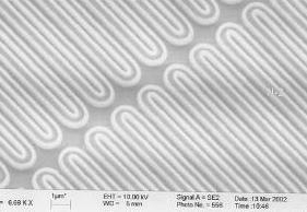
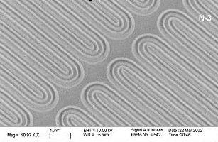
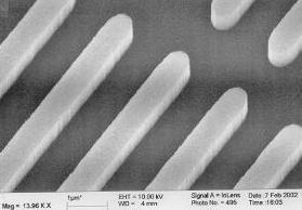
15 Spacer Lithography Definition Photo-lithographically defined sacrificial structures 1st Spacers 2nd Spacers 3rd Spacers 2 n lines after n iterations of spacer lithography! 15
16 Ioff, A/um Spacer Lithography: Small Impact 1.E-07 1.E-08 1.E-09 1.E-10 1.E-11 2x 10% Perfect 3nm 3s LWR 1.E-12 1.E-13 1.E-14 Perfect Fixed fin width with 1, 2, & 3nm waves Ion, ma/um 6nm 3s LWR 9nm 3s LWR 16
17 Spacer Lithography Imperfections Less deposition into small visibility angle <180 o 180 o 17
18 Spacer Lithography Imperfections Less deposition into small visibility angle Deposited layer (spacer) Dummy feature (top view) Deposition creates positive feedback, amplifying LER This gives you two edges that are in-sync (same phase), but different amplitudes Etching has the opposite, negative feedback, smoothing LER It might be possible to balance the deposition and etching effects, but Generally, spacer-litho-defined features will have some width variation 18
19 Ground Power Etch/Depo Micro-Loading Effects a b g NMOS PMOS PMOS Different fins experience different etch/deposition conditions Due to local visibility angles and pattern density This leads to variability in fin width and layer thicknesses 19
20 Ioff, A/um Imperfect Spacer Litho: Still OK 1.E-07 1.E-08 1.E-09 1.E-10 1.E-11 6x 12% Perfect Mid-thick 1.E-12 1.E-13 Perfect Fixed fin width with 1, 2, & 3nm waves 3nm waves+1nm fin width distortions Drain-thick 1.E Ion, ma/um Spacer litho is green : always reduces leakage! Mid-thin 20
21 Outline 21


22 Doping Random Dopant Fluctuations Gate Spacers As drain Source Drain As source Indium channel-stop Source Spacer Gate Spacer Drain 22
23 Ioff, A/um RDF: Insensitive to Junction Abruptness 1.E-06 1.E-07 1.E-08 Smooth 1nm/dec Atomistic 1nm/dec Smooth 3nm/dec Atomistic 3nm/dec 13mV s Vt 6mV s Vt Ion, ma/um Smooth junctions give similar performance for different amounts of abruptness The amount of RDF variability is quite moderate With junction abruptness degrading from 1nm/dec to 3nm/dec, s Vt only doubles Surprisingly low RDF sensitivity to junction abruptness Indium channel-stop RDF contribution is negligible 23


24 Ioff, A/um S/D RDF: Consistent with DL Variation 1.E-06 1.E-07 Smooth 1nm/dec Atomistic 1nm/dec Smooth 3nm/dec Atomistic 3nm/dec Top view of the fin: Indium below As As 11.2nm 13mV s Vt 1.E-08 6mV s Vt Ion, ma/um 12.6nm Apparent channel length difference is ~1.4nm S/D RDF are consistent with the DL sensitivity of 4x I off per 1nm 24
25 Ioff, A/um Single Dopant in the Channel: ~3e17 cm -3 1.E-06 Undoped channel One acceptor One donor Donor opens the channel for I off (3x), but not I on (3%) 1.E-07 Acceptor blocks the channel The impact is not catastrophic 1.E Ion, ma/um 25


26 Ioff, A/um Electrons wrap Single Dopant: Worst at Mid-Height 1.E-06 1.E-07 Undoped channel Top Middle Bottom around perimeter of the fin Electrons leak in the middle Top Middle Bottom I on I off Acceptors Donors 1.E Ion, ma/um Ions in the middle of the fin height affect I off the most Ions at the top of the fin affect I on the most Ions at the bottom of the fin have the least impact 26

27 Ioff, A/um Source Middle Drain Single Dopant: Worst at Mid-Length 1.E-06 1.E-07 Undoped channel Middle Source Drain Acceptors Donors 1.E Ion, ma/um Ions in the middle of the fin length have the most impact Ions at the source side have less impact Ions at the drain side have the least impact 27
28 Outline 28

29 Longitudinal Stress, GPa Hole Mobility Stress Enhancement Factor Stress Variation for Spacer Litho 0-1% -4% -8% 3 Stress and mobility values are averaged over the entire fin channel volume % +50% Before gate removal After metal gate Gate-first Gate-last Fin Wave Amplitude, nm Both the stress and the mobility increase upon poly removal Mobility enhancement degrades with fin curvature This adds (i.e. positive feedback) to the longer L with fin curvature 29


30 Longitudinal Stress, GPa Hole Mobility Stress Enhancement Factor Stress Variation for Distorted Spacer Litho -7% -4% Before poly gate removal for the gate-last HKMG, stress levels are very similar Before gate removal After metal gate Perfect Drain-thick Mid-thick Mid-thin However, after the poly removal, stress increases, but the amount is geometry-specific All non-rectangular shapes reduce mobility despite using the best patterning option: spacer lithography Gate-first HKMG has remarkably lower stress but remarkably lower stress variation 30


31 Non-Uniform Fin Stress Patterns -1 GPa -5 GPa Zero stress Huge stress variations, especially at the S/D junctions To get average fin stress of ~2 GPa, peak stress in the fin exceeds dangerous 5 GPa 31


32 High Shear Stress Levels High shear stress of ~1 GPa This is different from planar FETs Can affect mobility enhancement Can affect defect formation 32
33 Longitudinal Stress, GPa Hole Mobility Stress Enhancement Factor Gates DPT Mask Misalignment Impact on Stress Misalignment = 0nm 6nm 12nm Fins Mask #1 Mask #2-1% -5% Before gate removal After metal gate Gate-first Gate-last Mask Misalignment, nm Remarkably little stress loss even for major misalignment for gate-last HKMG Stronger effect for gate-first HKMG Again, perfect case performs the best Contact resistance will degrade much faster 33


34 Longitudinal Stress, GPa Hole Mobility Stress Enhancement Factor Gates DPT Mask Misalignment Impact on Stress Misalignment = 0nm 6nm 12nm Fins Mask #1 Mask #2-1% -5% Before gate removal After metal gate Gate-first Gate-last Mask Misalignment, nm Remarkably little stress loss even for major misalignment for gate-last HKMG Stronger effect for gate-first HKMG Again, perfect case performs the best Contact resistance will degrade much faster 34
35 Outline 35

36 Conclusions State-of-the-art litho is not good enough for fin and gate patterning Spacer lithography provides manageable amount of variations Geometry variation of +/- 1nm dominates variability over RDF & s S/D junction abruptness is not critical for performance & variability Single stray donor/acceptor dopant does not disturb performance significantly Remarkable stress gradients, from 5 GPa to 0 across the fin High shear stress levels, ~1 GPa 36
FLCC Seminar. Spacer Lithography for Reduced Variability in MOSFET Performance
 1 Seminar Spacer Lithography for Reduced Variability in MOSFET Performance Prof. Tsu-Jae King Liu Electrical Engineering & Computer Sciences Dept. University of California at Berkeley Graduate Student:
Simple and accurate modeling of the 3D structural variations in FinFETs
 Simple and accurate modeling of the 3D structural variations in FinFETs Donghu Kim Electrical Engineering Program Graduate school of UNIST 2013 Simple and accurate modeling of the 3D structural variations
EE115C Winter 2017 Digital Electronic Circuits. Lecture 3: MOS RC Model, CMOS Manufacturing
 EE115C Winter 2017 Digital Electronic Circuits Lecture 3: MOS RC Model, CMOS Manufacturing Agenda MOS Transistor: RC Model (pp. 104-113) S R on D CMOS Manufacturing Process (pp. 36-46) S S C GS G G C GD
Simulation-based Study of Super-steep Retrograde Doped Bulk FinFET Technology and 6T-SRAM Yield
 Simulation-based Study of Super-steep Retrograde Doped Bulk FinFET Technology and 6T-SRAM Yield Xi Zhang Electrical Engineering and Computer Sciences University of California at Berkeley Technical Report
ELEN0037 Microelectronic IC Design. Prof. Dr. Michael Kraft
 ELEN0037 Microelectronic IC Design Prof. Dr. Michael Kraft Lecture 2: Technological Aspects Technology Passive components Active components CMOS Process Basic Layout Scaling CMOS Technology Integrated
CHAPTER 5 EFFECT OF GATE ELECTRODE WORK FUNCTION VARIATION ON DC AND AC PARAMETERS IN CONVENTIONAL AND JUNCTIONLESS FINFETS
 98 CHAPTER 5 EFFECT OF GATE ELECTRODE WORK FUNCTION VARIATION ON DC AND AC PARAMETERS IN CONVENTIONAL AND JUNCTIONLESS FINFETS In this chapter, the effect of gate electrode work function variation on DC
Tri-Gate Fully-Depleted CMOS Transistors: Fabrication, Design and Layout
 Tri-Gate Fully-Depleted CMOS Transistors: Fabrication, Design and Layout B.Doyle, J.Kavalieros, T. Linton, R.Rios B.Boyanov, S.Datta, M. Doczy, S.Hareland, B. Jin, R.Chau Logic Technology Development Intel
The Pennsylvania State University. Kurt J. Lesker Company. North Carolina State University. Taiwan Semiconductor Manufacturing Company 1
 Enhancement Mode Strained (1.3%) Germanium Quantum Well FinFET (W fin =20nm) with High Mobility (μ Hole =700 cm 2 /Vs), Low EOT (~0.7nm) on Bulk Silicon Substrate A. Agrawal 1, M. Barth 1, G. B. Rayner
NANO-CMOS DESIGN FOR MANUFACTURABILILTY
 NANO-CMOS DESIGN FOR MANUFACTURABILILTY Robust Circuit and Physical Design for Sub-65nm Technology Nodes Ban Wong Franz Zach Victor Moroz An u rag Mittal Greg Starr Andrew Kahng WILEY A JOHN WILEY & SONS,
Faculty Presentation: Novel Technologies
 2009 IMPACT Workshop Faculty Presentation: Novel Technologies Chenming Hu, EECS Department, UC Berkeley Tsu-Jae King Liu, EECS Department, UC Berkeley Eugene Haller, MS&E Department, UC Berkeley Nathan
Ultimately Scaled CMOS: DG FinFETs?
 Ultimately Scaled CMOS: DG FinFETs? Jerry G. Fossum SOI Group Department of Electrical and Computer Engineering University of Florida Gainesville, FL 32611-6130 J. G. Fossum / 1 Outline Introduction -
Recent Development of FinFET Technology for CMOS Logic and Memory
 Recent Development of FinFET Technology for CMOS Logic and Memory Chung-Hsun Lin EECS Department University of California at Berkeley Why FinFET Outline FinFET process Unique features of FinFET Mobility,
Chapter 2 Process Variability. Overview. 2.1 Sources and Types of Variations
 Chapter 2 Process Variability Overview Parameter variability has always been an issue in integrated circuits. However, comparing with the size of devices, it is relatively increasing with technology evolution,
The Future of CMOS. David Pulfrey. CHRONOLOGY of the FET. Lecture Lilienfeld s patent (BG FET) 1965 Commercialization (Fairchild)
 1965 Commercialization (Fairchild)") The Future of CMOS David Pulfrey 1 CHRONOLOGY of the FET 1933 Lilienfeld s patent (BG FET) 1965 Commercialization (Fairchild) 1991 The most abundant object made by mankind (C.T. Sah) 2003 The 10 nm FET
The Future of CMOS David Pulfrey 1 CHRONOLOGY of the FET 1933 Lilienfeld s patent (BG FET) 1965 Commercialization (Fairchild) 1991 The most abundant object made by mankind (C.T. Sah) 2003 The 10 nm FET
EECS240 Spring Lecture 21: Matching. Elad Alon Dept. of EECS. V i+ V i-
 EECS40 Spring 010 Lecture 1: Matching Elad Alon Dept. of EECS Offset V i+ V i- To achieve zero offset, comparator devices must be perfectly matched to each other How well-matched can the devices be made?
L ECE 4211 UConn F. Jain Scaling Laws for NanoFETs Chapter 10 Logic Gate Scaling
 L13 04202017 ECE 4211 UConn F. Jain Scaling Laws for NanoFETs Chapter 10 Logic Gate Scaling Scaling laws: Generalized scaling (GS) p. 610 Design steps p.613 Nanotransistor issues (page 626) Degradation
Study of Carrier Transport in Strained and Unstrained SOI Tri-gate and Omega-gate Si Nanowire MOSFETs
 42nd ESSDERC, Bordeaux, France, 17-21 Sept. 2012 A2L-E, High Mobility Devices, 18 Sept. Study of Carrier Transport in Strained and Unstrained SOI Tri-gate and Omega-gate Si Nanowire MOSFETs M. Koyama 1,4,
EE410 vs. Advanced CMOS Structures
 EE410 vs. Advanced CMOS Structures Prof. Krishna S Department of Electrical Engineering S 1 EE410 CMOS Structure P + poly-si N + poly-si Al/Si alloy LPCVD PSG P + P + N + N + PMOS N-substrate NMOS P-well
Lecture 9. Strained-Si Technology I: Device Physics
 Strain Analysis in Daily Life Lecture 9 Strained-Si Technology I: Device Physics Background Planar MOSFETs FinFETs Reading: Y. Sun, S. Thompson, T. Nishida, Strain Effects in Semiconductors, Springer,
From Physics to Power, Performance, and Parasitics
 From Physics to Power, Performance, and Parasitics The GTS-Team Global TCAD Solutions GmbH, Böserndorferstraße 1/12, 1010 Vienna, Austria O. Baumgartner et al. (GTS) GTS 1 / 25 Scales, methods, hierarchies
Reliability of 3D IC with Via-Middle TSV: Characterization and Modeling
 Reliability of 3D IC with Via-Middle TSV: Characterization and Modeling Victor Moroz *, Munkang Choi *, Geert Van der Plas, Paul Marchal, Kristof Croes, and Eric Beyne * Motivation: Build Reliable 3D IC
Impact of parametric mismatch and fluctuations on performance and yield of deep-submicron CMOS technologies. Philips Research, The Netherlands
 Impact of parametric mismatch and fluctuations on performance and yield of deep-submicron CMOS technologies Hans Tuinhout, The Netherlands motivation: from deep submicron digital ULSI parametric spread
Self-Aligned InGaAs FinFETs with 5-nm Fin-Width and 5-nm Gate-Contact Separation
 Self-Aligned InGaAs FinFETs with 5-nm Fin-Width and 5-nm Gate-Contact Separation Alon Vardi, Lisa Kong, Wenjie Lu, Xiaowei Cai, Xin Zhao, Jesús Grajal* and Jesús A. del Alamo Microsystems Technology Laboratories,
ENABLEMENT OF COMPACT MODELS FOR
 ENABLEMENT OF COMPACT MODELS FOR ULTRA-SCALED CMOS TECHNOLOGIES D. YAKIMETS, P. SCHUDDINCK, D. JANG, M. GARCIA BARDON, N. SHARAN, B. PARVAIS*, P. RAGHAVAN, AND A. MOCUTA IMEC, KAPELDREEF 75, 3001 LEUVEN,
Multiple Gate CMOS and Beyond
 Multiple CMOS and Beyond Dept. of EECS, KAIST Yang-Kyu Choi Outline 1. Ultimate Scaling of MOSFETs - 3nm Nanowire FET - 8nm Non-Volatile Memory Device 2. Multiple Functions of MOSFETs 3. Summary 2 CMOS
Fig The electron mobility for a-si and poly-si TFT.
 Fig. 1-1-1 The electron mobility for a-si and poly-si TFT. Fig. 1-1-2 The aperture ratio for a-si and poly-si TFT. 33 Fig. 1-2-1 All kinds defect well. (a) is the Dirac well. (b) is the repulsive Columbic
Electronics The basics of semiconductor physics
 Electronics The basics of semiconductor physics Prof. Márta Rencz, Gergely Nagy BME DED September 16, 2013 The basic properties of semiconductors Semiconductors conductance is between that of conductors
Self-study problems and questions Processing and Device Technology, FFF110/FYSD13
 Self-study problems and questions Processing and Device Technology, FFF110/FYSD13 Version 2016_01 In addition to the problems discussed at the seminars and at the lectures, you can use this set of problems
Section 12: Intro to Devices
 Section 12: Intro to Devices Extensive reading materials on reserve, including Robert F. Pierret, Semiconductor Device Fundamentals EE143 Ali Javey Bond Model of Electrons and Holes Si Si Si Si Si Si Si
Semiconductor Physics fall 2012 problems
 Semiconductor Physics fall 2012 problems 1. An n-type sample of silicon has a uniform density N D = 10 16 atoms cm -3 of arsenic, and a p-type silicon sample has N A = 10 15 atoms cm -3 of boron. For each
Section 12: Intro to Devices
 Section 12: Intro to Devices Extensive reading materials on reserve, including Robert F. Pierret, Semiconductor Device Fundamentals Bond Model of Electrons and Holes Si Si Si Si Si Si Si Si Si Silicon
Enhanced Mobility CMOS
 Enhanced Mobility CMOS Judy L. Hoyt I. Åberg, C. Ni Chléirigh, O. Olubuyide, J. Jung, S. Yu, E.A. Fitzgerald, and D.A. Antoniadis Microsystems Technology Laboratory MIT, Cambridge, MA 02139 Acknowledge
ESE 570: Digital Integrated Circuits and VLSI Fundamentals
 ESE 570: Digital Integrated Circuits and VLSI Fundamentals Lec 4: January 23, 2018 MOS Transistor Theory, MOS Model Penn ESE 570 Spring 2018 Khanna Lecture Outline! CMOS Process Enhancements! Semiconductor
Scaling Issues in Planar FET: Dual Gate FET and FinFETs
 Scaling Issues in Planar FET: Dual Gate FET and FinFETs Lecture 12 Dr. Amr Bayoumi Fall 2014 Advanced Devices (EC760) Arab Academy for Science and Technology - Cairo 1 Outline Scaling Issues for Planar
Thin Film Transistors (TFT)
") Thin Film Transistors (TFT) a-si TFT - α-si:h (Hydrogenated amorphous Si) deposited with a PECVD system (low temp. process) replaces the single crystal Si substrate. - Inverted staggered structure with
Thin Film Transistors (TFT) a-si TFT - α-si:h (Hydrogenated amorphous Si) deposited with a PECVD system (low temp. process) replaces the single crystal Si substrate. - Inverted staggered structure with
ESE 570: Digital Integrated Circuits and VLSI Fundamentals
 ESE 570: Digital Integrated Circuits and VLSI Fundamentals Lec 4: January 29, 2019 MOS Transistor Theory, MOS Model Penn ESE 570 Spring 2019 Khanna Lecture Outline! CMOS Process Enhancements! Semiconductor
Modeling and Simulation of Variations in Nano-CMOS Design. Yun Ye
 Modeling and Simulation of Variations in Nano-CMOS Design by Yun Ye A Dissertation Presented in Partial Fulfillment of the Requirements for the Degree Doctor of Philosophy Approved April 2011 by the Graduate
A final review session will be offered on Thursday, May 10 from 10AM to 12noon in 521 Cory (the Hogan Room).
.") A final review session will be offered on Thursday, May 10 from 10AM to 12noon in 521 Cory (the Hogan Room). The Final Exam will take place from 12:30PM to 3:30PM on Saturday May 12 in 60 Evans.» All of
A final review session will be offered on Thursday, May 10 from 10AM to 12noon in 521 Cory (the Hogan Room). The Final Exam will take place from 12:30PM to 3:30PM on Saturday May 12 in 60 Evans.» All of
! CMOS Process Enhancements. ! Semiconductor Physics. " Band gaps. " Field Effects. ! MOS Physics. " Cut-off. " Depletion.
 ESE 570: Digital Integrated Circuits and VLSI Fundamentals Lec 4: January 9, 019 MOS Transistor Theory, MOS Model Lecture Outline CMOS Process Enhancements Semiconductor Physics Band gaps Field Effects
How a single defect can affect silicon nano-devices. Ted Thorbeck
 How a single defect can affect silicon nano-devices Ted Thorbeck tedt@nist.gov The Big Idea As MOS-FETs continue to shrink, single atomic scale defects are beginning to affect device performance Gate Source
Chapter 3 Basics Semiconductor Devices and Processing
 Chapter 3 Basics Semiconductor Devices and Processing Hong Xiao, Ph. D. www2.austin.cc.tx.us/hongxiao/book.htm Hong Xiao, Ph. D. www2.austin.cc.tx.us/hongxiao/book.htm 1 Objectives Identify at least two
Classification of Solids
 Classification of Solids Classification by conductivity, which is related to the band structure: (Filled bands are shown dark; D(E) = Density of states) Class Electron Density Density of States D(E) Examples
EECS240 Spring Today s Lecture. Lecture 2: CMOS Technology and Passive Devices. Lingkai Kong EECS. EE240 CMOS Technology
 EECS240 Spring 2013 Lecture 2: CMOS Technology and Passive Devices Lingkai Kong EECS Today s Lecture EE240 CMOS Technology Passive devices Motivation Resistors Capacitors (Inductors) Next time: MOS transistor
Chapter 4 Field-Effect Transistors
 Chapter 4 Field-Effect Transistors Microelectronic Circuit Design Richard C. Jaeger Travis N. Blalock 5/5/11 Chap 4-1 Chapter Goals Describe operation of MOSFETs. Define FET characteristics in operation
CMOS Technology for Computer Architects
 CMOS Technology for Computer Architects Recap Technology Trends Lecture 2: Transistor Inverter Iakovos Mavroidis Giorgos Passas Manolis Katevenis FORTH-ICS (University of Crete) 1 2 Recap Threshold Voltage
DIFFUSION - Chapter 7
 DIFFUSION - Chapter 7 Doping profiles determine many short-channel characteristics in MOS devices. Resistance impacts drive current. Scaling implies all lateral and vertical dimensions scale by the same
TCAD Modeling of Stress Impact on Performance and Reliability
 TCAD Modeling of Stress Impact on Performance and Reliability Xiaopeng Xu TCAD R&D, Synopsys March 16, 2010 SEMATECH Workshop on Stress Management for 3D ICs using Through Silicon Vias 1 Outline Introduction
UNIVERSITY OF CALIFORNIA College of Engineering Department of Electrical Engineering and Computer Sciences. Professor Oldham Fall 1999
 UNIVERSITY OF CLIFORNI College of Engineering Department of Electrical Engineering and Computer Sciences Professor Oldham Fall 1999 EECS 40 FINL EXM 13 December 1999 Name: Last, First Student ID: T: Kusuma
Introduction to Semiconductor Physics. Prof.P. Ravindran, Department of Physics, Central University of Tamil Nadu, India
 Introduction to Semiconductor Physics 1 Prof.P. Ravindran, Department of Physics, Central University of Tamil Nadu, India http://folk.uio.no/ravi/cmp2013 Review of Semiconductor Physics Semiconductor fundamentals
Lecture 5: CMOS Transistor Theory
 Lecture 5: CMOS Transistor Theory Slides courtesy of Deming Chen Slides based on the initial set from David Harris CMOS VLSI Design Outline q q q q q q q Introduction MOS Capacitor nmos I-V Characteristics
Simulation of Intrinsic Parameter Fluctuations in Decananometer and Nanometer-Scale MOSFETs
 IEEE TRANSACTIONS ON ELECTRON DEVICES, VOL. 50, NO. 9, SEPTEMBER 2003 1837 Simulation of Intrinsic Parameter Fluctuations in Decananometer and Nanometer-Scale MOSFETs Asen Asenov, Member, IEEE, Andrew
MOS Transistor I-V Characteristics and Parasitics
 ECEN454 Digital Integrated Circuit Design MOS Transistor I-V Characteristics and Parasitics ECEN 454 Facts about Transistors So far, we have treated transistors as ideal switches An ON transistor passes
Variability-Aware Compact Model Strategy for 20-nm Bulk MOSFET
 Variability-Aware Compact Model Strategy for 20-nm Bulk MOSFET X. Wang 1, D. Reid 2, L. Wang 1, A. Burenkov 3, C. Millar 2, B. Cheng 2, A. Lange 4, J. Lorenz 3, E. Baer 3, A. Asenov 1,2! 1 Device Modelling
Overview of Modeling and Simulation TCAD - FLOOPS / FLOODS
 Overview of Modeling and Simulation TCAD - FLOOPS / FLOODS Modeling Overview Strain Effects Thermal Modeling TCAD Modeling Outline FLOOPS / FLOODS Introduction Progress on GaN Devices Prospects for Reliability
Advanced and Emerging Devices: SEMATECH s Perspective
 SEMATECH Symposium October 23, 2012 Seoul Accelerating the next technology revolution Advanced and Emerging Devices: SEMATECH s Perspective Paul Kirsch Director, FEP Division Copyright 2012 SEMATECH, Inc.
Design/Technology Co-Optimisation (DTCO) in the Presence of Acute Variability
 in the Presence of Acute Variability") Design/Technology Co-Optimisation (DTCO) in the Presence of Acute Variability A. Asenov 1,2, E. A. Towie 1!! 1 Gold Standard Simulations Ltd 2 Glasgow University! Summary!! Introduction!! FinFET complexity
Design/Technology Co-Optimisation (DTCO) in the Presence of Acute Variability A. Asenov 1,2, E. A. Towie 1!! 1 Gold Standard Simulations Ltd 2 Glasgow University! Summary!! Introduction!! FinFET complexity
EE382M-14 CMOS Analog Integrated Circuit Design
 EE382M-14 CMOS Analog Integrated Circuit Design Lecture 3, MOS Capacitances, Passive Components, and Layout of Analog Integrated Circuits MOS Capacitances Type of MOS transistor capacitors Depletion capacitance
There's Plenty of Room at the Bottom
 There's Plenty of Room at the Bottom 12/29/1959 Feynman asked why not put the entire Encyclopedia Britannica (24 volumes) on a pin head (requires atomic scale recording). He proposed to use electron microscope
Piezoresistive Sensors
 Piezoresistive Sensors Outline Piezoresistivity of metal and semiconductor Gauge factor Piezoresistors Metal, silicon and polysilicon Close view of the piezoresistivity of single crystal silicon Considerations
A 20 nm gate-length ultra-thin body p-mosfet with silicide source/drain
 Superlattices and Microstructures, Vol. 28, No. 5/6, 2000 doi:10.1006/spmi.2000.0947 Available online at http://www.idealibrary.com on A 20 nm gate-length ultra-thin body p-mosfet with silicide source/drain
Extensive reading materials on reserve, including
 Section 12: Intro to Devices Extensive reading materials on reserve, including Robert F. Pierret, Semiconductor Device Fundamentals EE143 Ali Javey Bond Model of Electrons and Holes Si Si Si Si Si Si Si
ECE PN Junctions and Diodes
 ECE 342 2. PN Junctions and iodes Jose E. Schutt-Aine Electrical & Computer Engineering University of Illinois jschutt@emlab.uiuc.edu ECE 342 Jose Schutt Aine 1 B: material dependent parameter = 5.4 10
ELEC 4700 Assignment #2
 ELEC 4700 Assignment #2 Question 1 (Kasop 4.2) Molecular Orbitals and Atomic Orbitals Consider a linear chain of four identical atoms representing a hypothetical molecule. Suppose that each atomic wavefunction
! CMOS Process Enhancements. ! Semiconductor Physics. " Band gaps. " Field Effects. ! MOS Physics. " Cut-off. " Depletion.
 ESE 570: Digital Integrated Circuits and VLSI Fundamentals Lec 4: January 3, 018 MOS Transistor Theory, MOS Model Lecture Outline! CMOS Process Enhancements! Semiconductor Physics " Band gaps " Field Effects!
III-V CMOS: What have we learned from HEMTs? J. A. del Alamo, D.-H. Kim 1, T.-W. Kim, D. Jin, and D. A. Antoniadis
 III-V CMOS: What have we learned from HEMTs? J. A. del Alamo, D.-H. Kim 1, T.-W. Kim, D. Jin, and D. A. Antoniadis Microsystems Technology Laboratories, MIT 1 presently with Teledyne Scientific 23rd International
ECE 497 JS Lecture - 12 Device Technologies
 ECE 497 JS Lecture - 12 Device Technologies Spring 2004 Jose E. Schutt-Aine Electrical & Computer Engineering University of Illinois jose@emlab.uiuc.edu 1 NMOS Transistor 2 ρ Source channel charge density
Previously. ESE370: Circuit-Level Modeling, Design, and Optimization for Digital Systems. Today. Variation Types. Fabrication
 ESE370: Circuit-Level Modeling, Design, and Optimization for Digital Systems Previously Understand how to model transistor behavior Given that we know its parameters V dd, V th, t OX, C OX, W, L, N A Day
Diamond. Covalent Insulators and Semiconductors. Silicon, Germanium, Gray Tin. Chem 462 September 24, 2004
 Covalent Insulators and Chem 462 September 24, 2004 Diamond Pure sp 3 carbon All bonds staggered- ideal d(c-c) - 1.54 Å, like ethane Silicon, Germanium, Gray Tin Diamond structure Si and Ge: semiconductors
SPCC Department of Bio-Nano Technology and 2 Materials Science and Chemical Engineering, Hanyang University, Ansan, 15588, Republic of Korea.
 SPCC 2018 Hanyang University NEMPL Jin-Goo Park 1,2 *, Jung-Hwan Lee a, In-chan Choi 1, Hyun-Tae Kim 1, Lieve Teugels 3, and Tae-Gon Kim 3 1 Department of Bio-Nano Technology and 2 Materials Science and
Lecture 0: Introduction
 Lecture 0: Introduction Introduction q Integrated circuits: many transistors on one chip q Very Large Scale Integration (VLSI): bucketloads! q Complementary Metal Oxide Semiconductor Fast, cheap, low power
EECS130 Integrated Circuit Devices
 EECS130 Integrated Circuit Devices Professor Ali Javey 10/30/2007 MOSFETs Lecture 4 Reading: Chapter 17, 19 Announcements The next HW set is due on Thursday. Midterm 2 is next week!!!! Threshold and Subthreshold
Review of Semiconductor Fundamentals
 ECE 541/ME 541 Microelectronic Fabrication Techniques Review of Semiconductor Fundamentals Zheng Yang (ERF 3017, email: yangzhen@uic.edu) Page 1 Semiconductor A semiconductor is an almost insulating material,
CS 152 Computer Architecture and Engineering
 CS 152 Computer Architecture and Engineering Lecture 12 VLSI II 2005-2-24 John Lazzaro (www.cs.berkeley.edu/~lazzaro) TAs: Ted Hong and David Marquardt www-inst.eecs.berkeley.edu/~cs152/ Last Time: Device
ESE 570: Digital Integrated Circuits and VLSI Fundamentals
 ESE 570: Digital Integrated Circuits and VLSI Fundamentals Lec 4: January 24, 2017 MOS Transistor Theory, MOS Model Penn ESE 570 Spring 2017 Khanna Lecture Outline! Semiconductor Physics " Band gaps "
Lecture 4: CMOS Transistor Theory
 Introduction to CMOS VLSI Design Lecture 4: CMOS Transistor Theory David Harris, Harvey Mudd College Kartik Mohanram and Steven Levitan University of Pittsburgh Outline q Introduction q MOS Capacitor q
Chapter 13 Small-Signal Modeling and Linear Amplification
 Chapter 13 Small-Signal Modeling and Linear Amplification Microelectronic Circuit Design Richard C. Jaeger Travis N. Blalock 1/4/12 Chap 13-1 Chapter Goals Understanding of concepts related to: Transistors
The Devices: MOS Transistors
 The Devices: MOS Transistors References: Semiconductor Device Fundamentals, R. F. Pierret, Addison-Wesley Digital Integrated Circuits: A Design Perspective, J. Rabaey et.al. Prentice Hall NMOS Transistor
CS 152 Computer Architecture and Engineering. Lecture 11 VLSI
 CS 152 Computer Architecture and Engineering Lecture 11 VLSI 2005-10-6 John Lazzaro (www.cs.berkeley.edu/~lazzaro) TAs: David Marquardt and Udam Saini www-inst.eecs.berkeley.edu/~cs152/ Today: State Storage
MOS CAPACITOR AND MOSFET
 EE336 Semiconductor Devices 1 MOS CAPACITOR AND MOSFET Dr. Mohammed M. Farag Ideal MOS Capacitor Semiconductor Devices Physics and Technology Chapter 5 EE336 Semiconductor Devices 2 MOS Capacitor Structure
P. R. Nelson 1 ECE418 - VLSI. Midterm Exam. Solutions
 P. R. Nelson 1 ECE418 - VLSI Midterm Exam Solutions 1. (8 points) Draw the cross-section view for A-A. The cross-section view is as shown below.. ( points) Can you tell which of the metal1 regions is the
CMOS Cross Section. EECS240 Spring Today s Lecture. Dimensions. CMOS Process. Devices. Lecture 2: CMOS Technology and Passive Devices
 EECS240 Spring 2008 CMOS Cross Section Metal p - substrate p + diffusion Lecture 2: CMOS echnology and Passive Devices Poly n - well n + diffusion Elad Alon Dept. of EECS EECS240 Lecture 2 4 oday s Lecture
Digital Electronics Part II - Circuits
 Digital Electronics Part - Circuits Dr.. J. Wassell Gates from Transistors ntroduction Logic circuits are non-linear, consequently we will introduce a graphical technique for analysing such circuits The
Journal of Electron Devices, Vol. 18, 2013, pp JED [ISSN: ]
![Journal of Electron Devices, Vol. 18, 2013, pp JED [ISSN: ]](/thumbs/86/93990983.jpg "Journal of Electron Devices, Vol. 18, 2013, pp JED [ISSN: ]") DrainCurrent-Id in linearscale(a/um) Id in logscale Journal of Electron Devices, Vol. 18, 2013, pp. 1582-1586 JED [ISSN: 1682-3427 ] SUITABILITY OF HIGH-k GATE DIELECTRICS ON THE DEVICE PERFORMANCE AND
DrainCurrent-Id in linearscale(a/um) Id in logscale Journal of Electron Devices, Vol. 18, 2013, pp. 1582-1586 JED [ISSN: 1682-3427 ] SUITABILITY OF HIGH-k GATE DIELECTRICS ON THE DEVICE PERFORMANCE AND
LECTURE 3 MOSFETS II. MOS SCALING What is Scaling?
 LECTURE 3 MOSFETS II Lecture 3 Goals* * Understand constant field and constant voltage scaling and their effects. Understand small geometry effects for MOS transistors and their implications modeling and
CMOS Cross Section. EECS240 Spring Dimensions. Today s Lecture. Why Talk About Passives? EE240 Process
 EECS240 Spring 202 CMOS Cross Section Metal p - substrate p + diffusion Lecture 2: CMOS Technology and Passive Devices Poly n - well n + diffusion Elad Alon Dept. of EECS EECS240 Lecture 2 4 Today s Lecture
Semiconductors. Semiconductors also can collect and generate photons, so they are important in optoelectronic or photonic applications.
 Semiconductors Semiconducting materials have electrical properties that fall between true conductors, (like metals) which are always highly conducting and insulators (like glass or plastic or common ceramics)
Challenges in the introduction of Band to Band tunneling in semiclassical models for Tunnel-FETs. DIEGM - University of Udine, IU.
 Challenges in the introduction of Band to Band tunneling in semiclassical models for Tunnel-FETs, L.De Michielis*, M.Iellina and L.Selmi DIEGM - University of Udine, IU.NET *EPFL Outline Context Quantum
Lecture 15 OUTLINE. MOSFET structure & operation (qualitative) Review of electrostatics The (N)MOS capacitor
 Review of electrostatics The (N)MOS capacitor") Lecture 15 OUTLINE MOSFET structure & operation (qualitative) Review of electrostatics The (N)MOS capacitor Electrostatics Charge vs. voltage characteristic Reading: Chapter 6.1 6.2.1 EE15 Spring 28 Lecture
Lecture 15 OUTLINE MOSFET structure & operation (qualitative) Review of electrostatics The (N)MOS capacitor Electrostatics Charge vs. voltage characteristic Reading: Chapter 6.1 6.2.1 EE15 Spring 28 Lecture
Semiconductor Physics Problems 2015
 Semiconductor Physics Problems 2015 Page and figure numbers refer to Semiconductor Devices Physics and Technology, 3rd edition, by SM Sze and M-K Lee 1. The purest semiconductor crystals it is possible
Lecture Outline. ESE 570: Digital Integrated Circuits and VLSI Fundamentals. Review: MOSFET N-Type, P-Type. Semiconductor Physics.
 ESE 57: Digital Integrated Circuits and VLSI Fundamentals Lec 4: January 24, 217 MOS Transistor Theory, MOS Model Lecture Outline! Semiconductor Physics " Band gaps " Field Effects! MOS Physics " Cutoff
Lecture 2. Introduction to semiconductors Structures and characteristics in semiconductors. Fabrication of semiconductor sensor
 Lecture 2 Introduction to semiconductors Structures and characteristics in semiconductors Semiconductor p-n junction Metal Oxide Silicon structure Semiconductor contact Fabrication of semiconductor sensor
Next Time on Parametric Yield. What Drives Worst Case Analysis?
 Next Time on Parametric Yield Current and Advanced DFM techniques Worst Case Files The role of process simulation (TCAD) Complete Process Characterization Statistical Design The economics of DFM 1 What
Lecture 2. Introduction to semiconductors Structures and characteristics in semiconductors
 Lecture 2 Introduction to semiconductors Structures and characteristics in semiconductors Semiconductor p-n junction Metal Oxide Silicon structure Semiconductor contact Literature Glen F. Knoll, Radiation
This is the author s final accepted version.
 Al-Ameri, T., Georgiev, V.P., Adamu-Lema, F. and Asenov, A. (2017) Does a Nanowire Transistor Follow the Golden Ratio? A 2D Poisson- Schrödinger/3D Monte Carlo Simulation Study. In: 2017 International
Lecture 2. Introduction to semiconductors Structures and characteristics in semiconductors
 Lecture 2 Introduction to semiconductors Structures and characteristics in semiconductors Semiconductor p-n junction Metal Oxide Silicon structure Semiconductor contact Literature Glen F. Knoll, Radiation
The PSP compact MOSFET model An update
 The PSP compact MOSFET model An update Gert-Jan Smit, Andries Scholten, D.B.M. Klaassen NXP Semiconductors Ronald van Langevelde Philips Research Europe Gennady Gildenblat, Weimin Wu, Xin Li, Amit Jha,
Microelectronics Part 1: Main CMOS circuits design rules
 GBM8320 Dispositifs Médicaux telligents Microelectronics Part 1: Main CMOS circuits design rules Mohamad Sawan et al. Laboratoire de neurotechnologies Polystim! http://www.cours.polymtl.ca/gbm8320/! med-amine.miled@polymtl.ca!
Surfaces, Interfaces, and Layered Devices
 Surfaces, Interfaces, and Layered Devices Building blocks for nanodevices! W. Pauli: God made solids, but surfaces were the work of Devil. Surfaces and Interfaces 1 Interface between a crystal and vacuum
Field effect = Induction of an electronic charge due to an electric field Example: Planar capacitor
 JFETs AND MESFETs Introduction Field effect = Induction of an electronic charge due to an electric field Example: Planar capacitor Why would an FET made of a planar capacitor with two metal plates, as
Prospects for Ge MOSFETs
 Prospects for Ge MOSFETs Sematech Workshop December 4, 2005 Dimitri A. Antoniadis Microsystems Technology Laboratories MIT Sematech Workshop 2005 1 Channel Transport - I D I D =WQ i (x 0 )v xo v xo : carrier