Reliability of 3D IC with Via-Middle TSV: Characterization and Modeling
|
|
|
- Elijah Weaver
- 6 years ago
- Views:
Transcription

1 Reliability of 3D IC with Via-Middle TSV: Characterization and Modeling Victor Moroz *, Munkang Choi *, Geert Van der Plas, Paul Marchal, Kristof Croes, and Eric Beyne *


2 Motivation: Build Reliable 3D IC Technology From product idea... Mobile wide IO on logic ~1k TSV 1-2 layers DRAM...to integrated prototype LOGIC Logic die FCBGA substrate LOGIC TSV Backside RDL and Cu µbump Cu µbump SnAg Cu µbump Backside Polymer isolation DRAM DRAM 1
3 3D-Reliability Domains TSV TSV and its environment Stacking Chip Package Interaction Backside Processing 2
4 3D-Reliability Domains TSV TSV and its environment Stacking Chip Package Interaction Backside Processing 3


5 TSV Process Flow via etch oxide liner barrier seed Cu ECD Fill TSV anneal & CMP Top Liner PMD STI Si 5µm Middle Bottom 4


6 Cu Chemistry Impact on Cu Stress 3 Cu chemistries were studied: A, B, and C Chemistry A Chemistry B Chemistry C Chemistry C shows 3 times higher stress exhibits more elastic response 5


7 Cu Chemistry Impact on Cu Grains Chemistry A Chemistry B Chemistry C As deposited Cu film After sintering temperature cycling Grain growth Grain growth No significant 50um grain growth 6


8 Annealing Impact on Cu Properties To understand the evolution of the material response of Cu-TSV w.r.t the applied thermal treatment. Test performed by nano-indentation 7
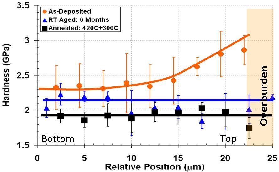
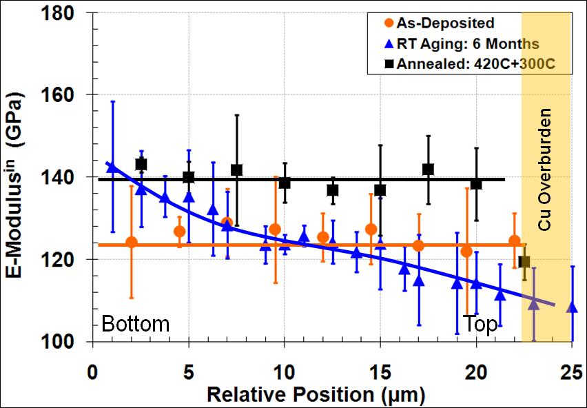
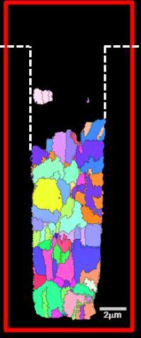
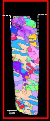
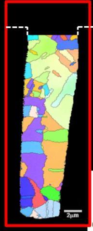
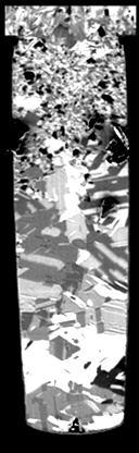
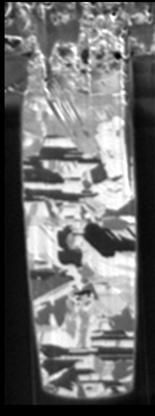
9 Cu Properties Evolution Nano-Indentation Top FIB Bottom Top EBSD Bottom 8
10 Control of Copper Pumping Model Does the pumping damage barrier oxide and brings charges/traps there? 9

11 Capacitance TSV Parasitic Capacitance 0 C w/o Nit C with Nit Q f Q it VTSV, V Effect of Interface states on MOS C-V... Can we control the oxide charges reliably?... Is the method repeatable and reliable? Interface trapped Charges (Q it ): Exist at the Si-SiO 2 interface Negative interface states cause undesired C-V shift Fixed Oxide Charges (Q f ): Exist near the Si-SiO 2 interface Positive fixed oxide charges cause desired C-V shift Oxide Trapped Charges: May exist in the entire oxide Positive trapped oxide charges cause desired C-V shift Negative trapped oxide charges cause undesired C-V shift Mobile Ionic Charge (Q m ): Undesirable Source: Physics of Semiconductor Devices by S. M. Sze 10
12 TSV Capacitance [ff] Thermo-Cycling Impact on TSV CV TC = 0 TC = 200 TC = 1000 QuasiStatic TC = 0 QuasiStatic TC = 200 QuasiStatic TC = 1000 T = 25 o C; Freq. = 100kHz-1MHz TSV Voltage [V] Thermo cycling: -40 o C (15 min) +125 o C (15 min) No significant change in TSV C-V behavior before and after thermo-cycling 11
13 CV-t: Detect Barrier Integrity Issues Lifetime of carriers is extracted from slope Change of lifetime is indicating Cu migration into Si 12
14 TSV Capacitance [ff] TSV Capacitance [ff] Thermo-Cycling Impact on C-t Freq = 1KHz-10KHz Freq = 10KHz-100KHz Freq = 100KHz-1MHz Quasi Static Temp = 25 o C TSV Voltage [V] TC = 0 TC = 200 TC = 1000 T = 25 o C; Freq. = 100kHz-1MHz Barrier Integrity preserved after thermo cycling Charges in oxide useful for capacitance reduction are harmless and do not deteriorate C- V and C-t behavior after thermocycling Time [sec] No significant change in TSV C-t behavior before and after thermo-cycling 13
15 3D-Reliability Domains TSV TSV and its environment Stacking Chip Package Interaction Backside Processing 14


16 Control of Copper Pumping Model Does the pumping damage interconnects above it? 15
17 R [Ohm] Resistance R [Ohm] TSV impact on M1 M1 meanders around TSVs OPEN ME1 ME2 ME3 ME4 M2 Top M1 Meanders with and without TSVs RES_M2_TSV RES_M2 OPEN_RES_M1-M2_TSV OPEN_RES_M1-M2 M1 Meanders M1 Top No evident impact of TSV Percent % Percent 16
18 Resistance R [Ohm] R [Ohm] TSV impact on M2 M2 meander-fork structures running above TSVs M2 (Top Die) meander-fork OPEN RES. MF AND TSV OPEN RES. MF WITH TSV OPEN RES. MF RES. MF WITH TSV RES. MF 10 4 TSV with starting pad in M1 (Top Die) No evident impact of TSV Percent % 17
19 Delta Ion, % Delta Ion, % TSV Stress Impact on Transistors 6 Transverse Direction 1 Longitudinal Direction Distance From TSV Along Y, um Distance From TSV Along X, um Good agreement of model and Si data No fitting necessary, just using measured Cu properties 18
20 Temperature Impact on TSV Stress Stress drops with temperature: Cu/Si thermal mismatch Linear trend suggests elastic stress behavior Will storage/operation temperature affect this? 19
21 Temperature Impact on TSV Stress Test approach Measure I on before and after thermal storage and cycling Test material HKMG gate stack CMOS technology TSV s: 5mm wide, 40mm deep Two splits in plating chemistry (Chem. D and Chem. E) Test structure Long channel pmos devices (from DAC Array) Reference transistors: > 20mm away from TSV Transistors close to TSV: 1.7mm away from TSV Today: Focus on transitors below TSV (i.e. transverse) 20
22 Ion change of device next to TSV (%) Equivalent Zero Stress Temperature ( C) Temperature Impact on TSV Stress Results before aging ºC ºC 80ºC 80ºC ºC 1 Chem. D Chem. E Chem. D Chem. E 120 Proposed aging tests 1 week at 175ºC ( ezst for chem. D and ezst for chem. E) 150 cycles between -45ºC and 125ºC 21
23 Ratio Temperature Impact on TSV Stress Results after aging 1.5 Proposed parameter: Ratio between %- difference before and after thermal stress T-storage below ezst (chem. D) 0.9 Stress increases T-storage above ezst (chem. E) Stress reduces 0.8 Chem. D T-Storage Chem. D T-Cycle Chem. E T-Storage T-cycling has even bigger impact 22
24 3D-Reliability Domains TSV TSV and its environment Stacking Chip Package Interaction Backside Processing 23
25 3D Stacking Approaches Die-to-wafer bonding approach: fast and accurate pick-and-place step, followed by collective bonding. Process of Record: Cu/Sn Scaling: 40 20µm Cu/Sn Transient-Liquid-Phase, TLP, (250 C) Diffusion bonding (150 C) 24
26 Micro-Bump Impact on N-FET Array BEOL FET array with ubump REF FET array Objective 25um LOGIC Determine Impact of ubump on long channel N-type logic devices Method Dummy ubump LOGIC NUF FEOL Compare Ion of Ref FET array with ubump FET array on stacked dies w/wo NUF 3.62 Device size = 800 x 600nm x16 FET array


27 Micro-Bump Impact on N-FETs Ubump REF FET w/o Ubump REF I ON Column Row FET with Ubump Normalized I ON vs REF Column Row Huge, 40% NMOS current impact! 26


28 Under-Fill Impact on N-FETs ETNA stacks with NUF 1 Cross-section for comparison ETNA stacks w/o NUF Row Row Column Column No underfill no stress 27
29 Normalized Ion wrt REF Cross-Section for FETs Above Ubump MOSFET # in row 6 of the array Si: w/o NUF Model Si: with NUF This effect is easy to model There is apparent ubump misalignment Combination of ubump and NUF has been identified as the main contributor of stress on thinned dies (25um) Stress induced by ubump w/o NEF on the FEOL is around 5% 28

30 Normalized Ion change wrt reference Ubump Stress at Elevated T FET Column FET Column x deg 60 deg 80 deg MOS position in row 6 of FET array Cross-section on FET row 6 Stress drops with temperature 29
31 Normalized Ion Change wrt Reference Ubump Stress vs Temperature Linear extrapolation shows 55% change at 0 degrees Close to linear change of Ion versus T from 25 0 to 80 0 C y = x Temperature, o C equivalent Zero Stress Temperature (ezst) is around Celsius Stress drops with temperature: Cu/NUF thermal mismatch Linear trend suggests elastic stress behavior 30
 Valley bottom (biaxial compr.) Hill top (biaxial tensile) Saddle point (compr.")
32 Modeling Micro-Bump Stress Saddle point (tensile Sxx but compr. Syy) Valley bottom (biaxial compr.) Hill top (biaxial tensile) Saddle point (compr. Sxx but zero Syy) 31
33 Modeling Micro-Bump Stress Map of vertical displacement (vertical scale exaggerated) Non-circular features due to anisotropic Si crystal properties Hills over m-bumps, valleys in between 32
34 Electron Mobility Map: 48% Range Strong hills, weak saddles, neutral valleys +42% -6% 33
35 Hole Mobility Map: 77% Range! Strong longitudinal saddles, weak transverse saddles, but neutral hills and valleys +31% -46% 34


36 Summary 35

37
TCAD Modeling of Stress Impact on Performance and Reliability
 TCAD Modeling of Stress Impact on Performance and Reliability Xiaopeng Xu TCAD R&D, Synopsys March 16, 2010 SEMATECH Workshop on Stress Management for 3D ICs using Through Silicon Vias 1 Outline Introduction
Thermal aspects of 3D and 2.5D integration
 Thermal aspects of 3D and 2.5D integration Herman Oprins Sr. Researcher Thermal Management - imec Co-authors: Vladimir Cherman, Geert Van der Plas, Eric Beyne European 3D Summit 23-25 January 2017 Grenoble,
Thin Film Transistors (TFT)
") Thin Film Transistors (TFT) a-si TFT - α-si:h (Hydrogenated amorphous Si) deposited with a PECVD system (low temp. process) replaces the single crystal Si substrate. - Inverted staggered structure with
Thin Film Transistors (TFT) a-si TFT - α-si:h (Hydrogenated amorphous Si) deposited with a PECVD system (low temp. process) replaces the single crystal Si substrate. - Inverted staggered structure with
Chapter 3 Basics Semiconductor Devices and Processing
 Chapter 3 Basics Semiconductor Devices and Processing Hong Xiao, Ph. D. www2.austin.cc.tx.us/hongxiao/book.htm Hong Xiao, Ph. D. www2.austin.cc.tx.us/hongxiao/book.htm 1 Objectives Identify at least two
Thermo-structural Model of Stacked Field-programmable Gate Arrays (FPGAs) with Through-silicon Vias (TSVs)
 with Through-silicon Vias (TSVs)") Manuscript for Review Thermo-structural Model of Stacked Field-programmable Gate Arrays (FPGAs) with Through-silicon Vias (TSVs) Journal: Electronics Letters Manuscript ID: draft Manuscript Type: Letter
Manuscript for Review Thermo-structural Model of Stacked Field-programmable Gate Arrays (FPGAs) with Through-silicon Vias (TSVs) Journal: Electronics Letters Manuscript ID: draft Manuscript Type: Letter
EE 292L : Nanomanufacturing. Week 5: Advanced Process Technology. Oct
 EE 292L : Nanomanufacturing Week 5: Advanced Process Technology Oct 22 2012 1 Advanced Process Technology 1 HAR etch 2 3 HAR Gapfill Metal ALD 4 Reflow 5 6 SAC Airgap 7 8 Strain Ge/III-V Engineering 1
MOS Transistor Properties Review
 MOS Transistor Properties Review 1 VLSI Chip Manufacturing Process Photolithography: transfer of mask patterns to the chip Diffusion or ion implantation: selective doping of Si substrate Oxidation: SiO
Research Challenges and Opportunities. in 3D Integrated Circuits. Jan 30, 2009
 Jan 3, 29 Research Challenges and Opportunities in 3D Integrated Circuits Ankur Jain ankur.jain@freescale.com, ankurjain@stanfordalumni.org Freescale Semiconductor, Inc. 28. 1 What is Three-dimensional
Lecture 6 PN Junction and MOS Electrostatics(III) Metal-Oxide-Semiconductor Structure
 Metal-Oxide-Semiconductor Structure") Lecture 6 PN Junction and MOS Electrostatics(III) Metal-Oxide-Semiconductor Structure Outline 1. Introduction to MOS structure 2. Electrostatics of MOS in thermal equilibrium 3. Electrostatics of MOS with
Lecture 6 PN Junction and MOS Electrostatics(III) Metal-Oxide-Semiconductor Structure Outline 1. Introduction to MOS structure 2. Electrostatics of MOS in thermal equilibrium 3. Electrostatics of MOS with
CMPEN 411 VLSI Digital Circuits. Lecture 03: MOS Transistor
 CMPEN 411 VLSI Digital Circuits Lecture 03: MOS Transistor Kyusun Choi [Adapted from Rabaey s Digital Integrated Circuits, Second Edition, 2003 J. Rabaey, A. Chandrakasan, B. Nikolic] CMPEN 411 L03 S.1
MOSFET: Introduction
 E&CE 437 Integrated VLSI Systems MOS Transistor 1 of 30 MOSFET: Introduction Metal oxide semiconductor field effect transistor (MOSFET) or MOS is widely used for implementing digital designs Its major
Lecture 0: Introduction
 Lecture 0: Introduction Introduction q Integrated circuits: many transistors on one chip q Very Large Scale Integration (VLSI): bucketloads! q Complementary Metal Oxide Semiconductor Fast, cheap, low power
EE 434 Lecture 12. Process Flow (wrap up) Device Modeling in Semiconductor Processes
 Device Modeling in Semiconductor Processes") EE 434 Lecture 12 Process Flow (wrap up) Device Modeling in Semiconductor Processes Quiz 6 How have process engineers configured a process to assure that the thickness of the gate oxide for the p-channel
EE 434 Lecture 12 Process Flow (wrap up) Device Modeling in Semiconductor Processes Quiz 6 How have process engineers configured a process to assure that the thickness of the gate oxide for the p-channel
Lecture 12: MOS Capacitors, transistors. Context
 Lecture 12: MOS Capacitors, transistors Context In the last lecture, we discussed PN diodes, and the depletion layer into semiconductor surfaces. Small signal models In this lecture, we will apply those
The Devices. Digital Integrated Circuits A Design Perspective. Jan M. Rabaey Anantha Chandrakasan Borivoje Nikolic. July 30, 2002
 igital Integrated Circuits A esign Perspective Jan M. Rabaey Anantha Chandrakasan Borivoje Nikolic The evices July 30, 2002 Goal of this chapter Present intuitive understanding of device operation Introduction
ECE 340 Lecture 39 : MOS Capacitor II
 ECE 340 Lecture 39 : MOS Capacitor II Class Outline: Effects of Real Surfaces Threshold Voltage MOS Capacitance-Voltage Analysis Things you should know when you leave Key Questions What are the effects
Operation and Modeling of. The MOS Transistor. Second Edition. Yannis Tsividis Columbia University. New York Oxford OXFORD UNIVERSITY PRESS
 Operation and Modeling of The MOS Transistor Second Edition Yannis Tsividis Columbia University New York Oxford OXFORD UNIVERSITY PRESS CONTENTS Chapter 1 l.l 1.2 1.3 1.4 1.5 1.6 1.7 Chapter 2 2.1 2.2
Section 12: Intro to Devices
 Section 12: Intro to Devices Extensive reading materials on reserve, including Robert F. Pierret, Semiconductor Device Fundamentals EE143 Ali Javey Bond Model of Electrons and Holes Si Si Si Si Si Si Si
The Devices. Jan M. Rabaey
 The Devices Jan M. Rabaey Goal of this chapter Present intuitive understanding of device operation Introduction of basic device equations Introduction of models for manual analysis Introduction of models
Fundamentals of the Metal Oxide Semiconductor Field-Effect Transistor
 Triode Working FET Fundamentals of the Metal Oxide Semiconductor Field-Effect Transistor The characteristics of energy bands as a function of applied voltage. Surface inversion. The expression for the
Gold Nanoparticles Floating Gate MISFET for Non-Volatile Memory Applications
 Gold Nanoparticles Floating Gate MISFET for Non-Volatile Memory Applications D. Tsoukalas, S. Kolliopoulou, P. Dimitrakis, P. Normand Institute of Microelectronics, NCSR Demokritos, Athens, Greece S. Paul,
Benefits of Stacked-Wafer Capacitors for High-Frequency Buck Converters
 Benefits of Stacked-Wafer Capacitors for High-Frequency Buck Converters Michael W. Baker, PhD Maxim Integrated Power SoC Northeastern University, Boston MA. October 7, 2014 Mobile Device Trends Power Management
Today s lecture. EE141- Spring 2003 Lecture 4. Design Rules CMOS Inverter MOS Transistor Model
 - Spring 003 Lecture 4 Design Rules CMOS Inverter MOS Transistor Model Today s lecture Design Rules The CMOS inverter at a glance An MOS transistor model for manual analysis Important! Labs start next
Chapter 2. Design and Fabrication of VLSI Devices
 Chapter 2 Design and Fabrication of VLSI Devices Jason Cong 1 Design and Fabrication of VLSI Devices Objectives: To study the materials used in fabrication of VLSI devices. To study the structure of devices
Classification of Solids
 Classification of Solids Classification by conductivity, which is related to the band structure: (Filled bands are shown dark; D(E) = Density of states) Class Electron Density Density of States D(E) Examples
The Devices. Digital Integrated Circuits A Design Perspective. Jan M. Rabaey Anantha Chandrakasan Borivoje Nikolic. July 30, 2002
 Digital Integrated Circuits A Design Perspective Jan M. Rabaey Anantha Chandrakasan Borivoje Nikolic The Devices July 30, 2002 Goal of this chapter Present intuitive understanding of device operation Introduction
FEM Analysis on Mechanical Stress of 2.5D Package Interposers
 Hisada et al.: FEM Analysis on Mechanical Stress of 2.5D Package Interposers (1/8) [Technical Paper] FEM Analysis on Mechanical Stress of 2.5D Package Interposers Takashi Hisada, Toyohiro Aoki, Junko Asai,
Coupling Capacitance in Face-to-Face (F2F) Bonded 3D ICs: Trends and Implications
 Bonded 3D ICs: Trends and Implications") Coupling Capacitance in Face-to-Face (F2F) Bonded 3D ICs: Trends and Implications Taigon Song *1, Arthur Nieuwoudt *2, Yun Seop Yu *3 and Sung Kyu Lim *1 *1 School of Electrical and Computer Engineering,
Coupling Capacitance in Face-to-Face (F2F) Bonded 3D ICs: Trends and Implications Taigon Song *1, Arthur Nieuwoudt *2, Yun Seop Yu *3 and Sung Kyu Lim *1 *1 School of Electrical and Computer Engineering,
Section 12: Intro to Devices
 Section 12: Intro to Devices Extensive reading materials on reserve, including Robert F. Pierret, Semiconductor Device Fundamentals Bond Model of Electrons and Holes Si Si Si Si Si Si Si Si Si Silicon
SEMICONDUCTOR MEMORIES
 SEMICONDUCTOR MEMORIES Semiconductor Memory Classification RWM NVRWM ROM Random Access Non-Random Access EPROM E 2 PROM Mask-Programmed Programmable (PROM) SRAM FIFO FLASH DRAM LIFO Shift Register CAM
ENEE 359a Digital VLSI Design
 SLIDE 1 ENEE 359a Digital VLSI Design & Logical Effort Prof. blj@ece.umd.edu Credit where credit is due: Slides contain original artwork ( Jacob 2004) as well as material taken liberally from Irwin & Vijay
Choice of V t and Gate Doping Type
 Choice of V t and Gate Doping Type To make circuit design easier, it is routine to set V t at a small positive value, e.g., 0.4 V, so that, at V g = 0, the transistor does not have an inversion layer and
CMOS Cross Section. EECS240 Spring Dimensions. Today s Lecture. Why Talk About Passives? EE240 Process
 EECS240 Spring 202 CMOS Cross Section Metal p - substrate p + diffusion Lecture 2: CMOS Technology and Passive Devices Poly n - well n + diffusion Elad Alon Dept. of EECS EECS240 Lecture 2 4 Today s Lecture
Self-study problems and questions Processing and Device Technology, FFF110/FYSD13
 Self-study problems and questions Processing and Device Technology, FFF110/FYSD13 Version 2016_01 In addition to the problems discussed at the seminars and at the lectures, you can use this set of problems
Digital Integrated Circuits A Design Perspective. Jan M. Rabaey Anantha Chandrakasan Borivoje Nikolic. The Devices. July 30, Devices.
 Digital Integrated Circuits A Design Perspective Jan M. Rabaey Anantha Chandrakasan Borivoje Nikolic The July 30, 2002 1 Goal of this chapter Present intuitive understanding of device operation Introduction
CS 152 Computer Architecture and Engineering
 CS 152 Computer Architecture and Engineering Lecture 12 VLSI II 2005-2-24 John Lazzaro (www.cs.berkeley.edu/~lazzaro) TAs: Ted Hong and David Marquardt www-inst.eecs.berkeley.edu/~cs152/ Last Time: Device
ECE 342 Electronic Circuits. Lecture 6 MOS Transistors
 ECE 342 Electronic Circuits Lecture 6 MOS Transistors Jose E. Schutt-Aine Electrical & Computer Engineering University of Illinois jesa@illinois.edu 1 NMOS Transistor Typically L = 0.1 to 3 m, W = 0.2
EE115C Winter 2017 Digital Electronic Circuits. Lecture 3: MOS RC Model, CMOS Manufacturing
 EE115C Winter 2017 Digital Electronic Circuits Lecture 3: MOS RC Model, CMOS Manufacturing Agenda MOS Transistor: RC Model (pp. 104-113) S R on D CMOS Manufacturing Process (pp. 36-46) S S C GS G G C GD
CMOS INVERTER. Last Lecture. Metrics for qualifying digital circuits. »Cost» Reliability» Speed (delay)»performance
»performance") CMOS INVERTER Last Lecture Metrics for qualifying digital circuits»cost» Reliability» Speed (delay)»performance 1 Today s lecture The CMOS inverter at a glance An MOS transistor model for manual analysis
CMOS INVERTER Last Lecture Metrics for qualifying digital circuits»cost» Reliability» Speed (delay)»performance 1 Today s lecture The CMOS inverter at a glance An MOS transistor model for manual analysis
Thermal-reliable 3D Clock-tree Synthesis Considering Nonlinear Electrical-thermal-coupled TSV Model
 Thermal-reliable 3D Clock-tree Synthesis Considering Nonlinear Electrical-thermal-coupled TSV Model Yang Shang 1, Chun Zhang 1, Hao Yu 1, Chuan Seng Tan 1, Xin Zhao 2, Sung Kyu Lim 2 1 School of Electrical
ECE520 VLSI Design. Lecture 8: Interconnect Manufacturing and Modeling. Payman Zarkesh-Ha
 ECE520 VLSI Design Lecture 8: Interconnect Manufacturing and Modeling Payman Zarkesh-Ha Office: ECE Bldg. 230B Office hours: Wednesday 2:00-3:00PM or by appointment E-mail: pzarkesh@unm.edu Slide: 1 Review
Electronics with 2D Crystals: Scaling extender, or harbinger of new functions?
 Electronics with 2D Crystals: Scaling extender, or harbinger of new functions? 1 st Workshop on Data Abundant Systems Technology Stanford, April 2014 Debdeep Jena (djena@nd.edu) Electrical Engineering,
Semiconductor Devices. C. Hu: Modern Semiconductor Devices for Integrated Circuits Chapter 5
 Semiconductor Devices C. Hu: Modern Semiconductor Devices for Integrated Circuits Chapter 5 Global leader in environmental and industrial measurement Wednesday 3.2. afternoon Tour around facilities & lecture
Future trends in radiation hard electronics
 Future trends in radiation hard electronics F. Faccio CERN, Geneva, Switzerland Outline Radiation effects in CMOS technologies Deep submicron CMOS for radiation environments What is the future going to
EE382M-14 CMOS Analog Integrated Circuit Design
 EE382M-14 CMOS Analog Integrated Circuit Design Lecture 3, MOS Capacitances, Passive Components, and Layout of Analog Integrated Circuits MOS Capacitances Type of MOS transistor capacitors Depletion capacitance
Performance Enhancement of P-channel InGaAs Quantum-well FETs by Superposition of Process-induced Uniaxial Strain and Epitaxially-grown Biaxial Strain
 Performance Enhancement of P-channel InGaAs Quantum-well FETs by Superposition of Process-induced Uniaxial Strain and Epitaxially-grown Biaxial Strain Ling Xia 1, Vadim Tokranov 2, Serge R. Oktyabrsky
MOS CAPACITOR AND MOSFET
 EE336 Semiconductor Devices 1 MOS CAPACITOR AND MOSFET Dr. Mohammed M. Farag Ideal MOS Capacitor Semiconductor Devices Physics and Technology Chapter 5 EE336 Semiconductor Devices 2 MOS Capacitor Structure
EV Group. Engineered Substrates for future compound semiconductor devices
 EV Group Engineered Substrates for future compound semiconductor devices Engineered Substrates HB-LED: Engineered growth substrates GaN / GaP layer transfer Mobility enhancement solutions: III-Vs to silicon
Electrical Characterization of 3D Through-Silicon-Vias
 Electrical Characterization of 3D Through-Silicon-Vias F. Liu, X. u, K. A. Jenkins, E. A. Cartier, Y. Liu, P. Song, and S. J. Koester IBM T. J. Watson Research Center Yorktown Heights, NY 1598, USA Phone:
EE143 LAB. Professor N Cheung, U.C. Berkeley
 EE143 LAB 1 1 EE143 Equipment in Cory 218 2 Guidelines for Process Integration * A sequence of Additive and Subtractive steps with lateral patterning Processing Steps Si wafer Watch out for materials compatibility
ELECTROMAGNETIC MODELING OF THREE DIMENSIONAL INTEGRATED CIRCUITS MENTOR GRAPHICS
 ELECTROMAGNETIC MODELING OF THREE DIMENSIONAL INTEGRATED CIRCUITS MENTOR GRAPHICS H I G H S P E E D D E S I G N W H I T E P A P E R w w w. m e n t o r. c o m / p c b INTRODUCTION Three Dimensional Integrated
Equivalent Circuit Model Extraction for Interconnects in 3D ICs
 Equivalent Circuit Model Extraction for Interconnects in 3D ICs A. Ege Engin Assistant Professor, Department of ECE, San Diego State University Email: aengin@mail.sdsu.edu ASP-DAC, Jan. 23, 213 Outline
Semiconductor memories
 Semiconductor memories Semiconductor Memories Data in Write Memory cell Read Data out Some design issues : How many cells? Function? Power consuption? Access type? How fast are read/write operations? Semiconductor
AE74 VLSI DESIGN JUN 2015
 Q.2 a. Write down the different levels of integration of IC industry. (4) b. With neat sketch explain briefly PMOS & NMOS enhancement mode transistor. N-MOS enhancement mode transistor:- This transistor
EE 5211 Analog Integrated Circuit Design. Hua Tang Fall 2012
 EE 5211 Analog Integrated Circuit Design Hua Tang Fall 2012 Today s topic: 1. Introduction to Analog IC 2. IC Manufacturing (Chapter 2) Introduction What is Integrated Circuit (IC) vs discrete circuits?
ESE370: Circuit-Level Modeling, Design, and Optimization for Digital Systems
 ESE370: Circuit-Level Modeling, Design, and Optimization for Digital Systems Lec 6: September 18, 2017 MOS Model You are Here: Transistor Edition! Previously: simple models (0 and 1 st order) " Comfortable
EECS240 Spring Today s Lecture. Lecture 2: CMOS Technology and Passive Devices. Lingkai Kong EECS. EE240 CMOS Technology
 EECS240 Spring 2013 Lecture 2: CMOS Technology and Passive Devices Lingkai Kong EECS Today s Lecture EE240 CMOS Technology Passive devices Motivation Resistors Capacitors (Inductors) Next time: MOS transistor
Device Models (PN Diode, MOSFET )
") Device Models (PN Diode, MOSFET ) Instructor: Steven P. Levitan steve@ece.pitt.edu TA: Gayatri Mehta, José Martínez Book: Digital Integrated Circuits: A Design Perspective; Jan Rabaey Lab Notes: Handed
Device Models (PN Diode, MOSFET ) Instructor: Steven P. Levitan steve@ece.pitt.edu TA: Gayatri Mehta, José Martínez Book: Digital Integrated Circuits: A Design Perspective; Jan Rabaey Lab Notes: Handed
Microelectronics Part 1: Main CMOS circuits design rules
 GBM8320 Dispositifs Médicaux telligents Microelectronics Part 1: Main CMOS circuits design rules Mohamad Sawan et al. Laboratoire de neurotechnologies Polystim! http://www.cours.polymtl.ca/gbm8320/! med-amine.miled@polymtl.ca!
12/10/09. Chapter 18: Electrical Properties. View of an Integrated Circuit. Electrical Conduction ISSUES TO ADDRESS...
 Chapter 18: Electrical Properties ISSUES TO ADDRESS... How are electrical conductance and resistance characterized? What are the physical phenomena that distinguish? For metals, how is affected by and
Delamination Modeling for Power Packages and Modules. Rainer Dudek, R. Döring, S. Rzepka Fraunhofer ENAS, Micro Materials Center Chemnitz
 Delamination Modeling for Power Packages and Modules Rainer Dudek, R. Döring, S. Rzepka Fraunhofer ENAS, Micro Materials Center Chemnitz The Micro Materials Center @ Virtual Prototyping Finite Element
CVD: General considerations.
 CVD: General considerations. PVD: Move material from bulk to thin film form. Limited primarily to metals or simple materials. Limited by thermal stability/vapor pressure considerations. Typically requires
ISSUES TO ADDRESS...
 Chapter 12: Electrical Properties School of Mechanical Engineering Choi, Hae-Jin Materials Science - Prof. Choi, Hae-Jin Chapter 12-1 ISSUES TO ADDRESS... How are electrical conductance and resistance
MODEL MECHANISM OF CMOS DEVICE FOR RELIBILITY ENHANCEMENT
 MODEL MECHANISM OF CMOS DEVICE FOR RELIBILITY ENHANCEMENT Sandeep Lalawat and Prof.Y.S.Thakur lalawat_er2007@yahoo.co.in,ystgecu@yahoo.co.in Abstract This paper present specific device level life time
CHAPTER 5 EFFECT OF GATE ELECTRODE WORK FUNCTION VARIATION ON DC AND AC PARAMETERS IN CONVENTIONAL AND JUNCTIONLESS FINFETS
 98 CHAPTER 5 EFFECT OF GATE ELECTRODE WORK FUNCTION VARIATION ON DC AND AC PARAMETERS IN CONVENTIONAL AND JUNCTIONLESS FINFETS In this chapter, the effect of gate electrode work function variation on DC
Digital Integrated Circuits A Design Perspective
 Semiconductor Memories Adapted from Chapter 12 of Digital Integrated Circuits A Design Perspective Jan M. Rabaey et al. Copyright 2003 Prentice Hall/Pearson Outline Memory Classification Memory Architectures
Lecture 9. Strained-Si Technology I: Device Physics
 Strain Analysis in Daily Life Lecture 9 Strained-Si Technology I: Device Physics Background Planar MOSFETs FinFETs Reading: Y. Sun, S. Thompson, T. Nishida, Strain Effects in Semiconductors, Springer,
Multiple Gate CMOS and Beyond
 Multiple CMOS and Beyond Dept. of EECS, KAIST Yang-Kyu Choi Outline 1. Ultimate Scaling of MOSFETs - 3nm Nanowire FET - 8nm Non-Volatile Memory Device 2. Multiple Functions of MOSFETs 3. Summary 2 CMOS
MOS Transistor Theory
 MOS Transistor Theory So far, we have viewed a MOS transistor as an ideal switch (digital operation) Reality: less than ideal EE 261 Krish Chakrabarty 1 Introduction So far, we have treated transistors
Lecture 4: CMOS Transistor Theory
 Introduction to CMOS VLSI Design Lecture 4: CMOS Transistor Theory David Harris, Harvey Mudd College Kartik Mohanram and Steven Levitan University of Pittsburgh Outline q Introduction q MOS Capacitor q
Performance, Packaging, Price: Challenges for Sensor Research I. Eisele Fraunhofer EMFT
 Performance, Packaging, Price: Challenges for Sensor Research I. Eisele Fraunhofer EMFT Introduction There are many sensor effects... but only a a very few sensors! Outline CMOS Encapsulated CMOS/MEMS
VLSI Design and Simulation
 VLSI Design and Simulation Performance Characterization Topics Performance Characterization Resistance Estimation Capacitance Estimation Inductance Estimation Performance Characterization Inverter Voltage
Supporting Online Material for
 www.sciencemag.org/cgi/content/full/327/5966/662/dc Supporting Online Material for 00-GHz Transistors from Wafer-Scale Epitaxial Graphene Y.-M. Lin,* C. Dimitrakopoulos, K. A. Jenkins, D. B. Farmer, H.-Y.
ESE 570: Digital Integrated Circuits and VLSI Fundamentals
 ESE 570: Digital Integrated Circuits and VLSI Fundamentals Lec 4: January 29, 2019 MOS Transistor Theory, MOS Model Penn ESE 570 Spring 2019 Khanna Lecture Outline! CMOS Process Enhancements! Semiconductor
TRENDS IN LEVENSDUURTESTEN VOOR MICRO-ELEKTRONICA PLOT CONFERENTIE
 TRENDS IN LEVENSDUURTESTEN VOOR MICRO-ELEKTRONICA PLOT CONFERENTIE JEROEN JALINK 8 JUNI 2016 MICROELECTRONICS RELIABILITY 54 (2014) 1988 1994 Contents Introduction NXP Package form factor Failure mechanism
Lecture 3: CMOS Transistor Theory
 Lecture 3: CMOS Transistor Theory Outline Introduction MOS Capacitor nmos I-V Characteristics pmos I-V Characteristics Gate and Diffusion Capacitance 2 Introduction So far, we have treated transistors
ELEN0037 Microelectronic IC Design. Prof. Dr. Michael Kraft
 ELEN0037 Microelectronic IC Design Prof. Dr. Michael Kraft Lecture 2: Technological Aspects Technology Passive components Active components CMOS Process Basic Layout Scaling CMOS Technology Integrated
Digital Integrated Circuits A Design Perspective. Semiconductor. Memories. Memories
 Digital Integrated Circuits A Design Perspective Semiconductor Chapter Overview Memory Classification Memory Architectures The Memory Core Periphery Reliability Case Studies Semiconductor Memory Classification
Final Examination EE 130 December 16, 1997 Time allotted: 180 minutes
 Final Examination EE 130 December 16, 1997 Time allotted: 180 minutes Problem 1: Semiconductor Fundamentals [30 points] A uniformly doped silicon sample of length 100µm and cross-sectional area 100µm 2
Mitigating Semiconductor Hotspots
 Mitigating Semiconductor Hotspots The Heat is On: Thermal Management in Microelectronics February 15, 2007 Seri Lee, Ph.D. (919) 485-5509 slee@nextremethermal.com www.nextremethermal.com 1 Agenda Motivation
ESE370: Circuit-Level Modeling, Design, and Optimization for Digital Systems
 ESE370: Circuit-Level Modeling, Design, and Optimization for Digital Systems Lec 6: September 14, 2015 MOS Model You are Here: Transistor Edition! Previously: simple models (0 and 1 st order) " Comfortable
Moores Law for DRAM. 2x increase in capacity every 18 months 2006: 4GB
 MEMORY Moores Law for DRAM 2x increase in capacity every 18 months 2006: 4GB Corollary to Moores Law Cost / chip ~ constant (packaging) Cost / bit = 2X reduction / 18 months Current (2008) ~ 1 micro-cent
Interconnect (2) Buffering Techniques.Transmission Lines. Lecture Fall 2003
 Buffering Techniques.Transmission Lines. Lecture Fall 2003") Interconnect (2) Buffering Techniques.Transmission Lines Lecture 12 18-322 Fall 2003 A few announcements Partners Lab Due Times Midterm 1 is nearly here Date: 10/14/02, time: 3:00-4:20PM, place: in class
Interconnect (2) Buffering Techniques.Transmission Lines Lecture 12 18-322 Fall 2003 A few announcements Partners Lab Due Times Midterm 1 is nearly here Date: 10/14/02, time: 3:00-4:20PM, place: in class
Will Reliability Limit Moore s Law?
 Will Reliability Limit Moore s Law? Tony Oates, TSMC 1 Outline Trends Interconnect Transistors Soft Errors in Memory and Logic Conclusions 2 Market Growth Electronic Equipment Revenue ($B) 2,500 2,000
1 INTRODUCTION 2 SAMPLE PREPARATIONS
 Chikage NORITAKE This study seeks to analyze the reliability of three-dimensional (3D) chip stacked packages under cyclic thermal loading. The critical areas of 3D chip stacked packages are defined using
MENA9510 characterization course: Capacitance-voltage (CV) measurements
 measurements") MENA9510 characterization course: Capacitance-voltage (CV) measurements 30.10.2017 Halvard Haug Outline Overview of interesting sample structures Ohmic and schottky contacts Why C-V for solar cells? The
MENA9510 characterization course: Capacitance-voltage (CV) measurements 30.10.2017 Halvard Haug Outline Overview of interesting sample structures Ohmic and schottky contacts Why C-V for solar cells? The
SPCC Department of Bio-Nano Technology and 2 Materials Science and Chemical Engineering, Hanyang University, Ansan, 15588, Republic of Korea.
 SPCC 2018 Hanyang University NEMPL Jin-Goo Park 1,2 *, Jung-Hwan Lee a, In-chan Choi 1, Hyun-Tae Kim 1, Lieve Teugels 3, and Tae-Gon Kim 3 1 Department of Bio-Nano Technology and 2 Materials Science and
CS 152 Computer Architecture and Engineering. Lecture 11 VLSI
 CS 152 Computer Architecture and Engineering Lecture 11 VLSI 2005-10-6 John Lazzaro (www.cs.berkeley.edu/~lazzaro) TAs: David Marquardt and Udam Saini www-inst.eecs.berkeley.edu/~cs152/ Today: State Storage
Lecture 25. Semiconductor Memories. Issues in Memory
 Lecture 25 Semiconductor Memories Issues in Memory Memory Classification Memory Architectures TheMemoryCore Periphery 1 Semiconductor Memory Classification RWM NVRWM ROM Random Access Non-Random Access
Lecture 5 Fault Modeling
 Lecture 5 Fault Modeling Why model faults? Some real defects in VLSI and PCB Common fault models Stuck-at faults Single stuck-at faults Fault equivalence Fault dominance and checkpoint theorem Classes
Chapter 12: Electrical Properties. RA l
 Charge carriers and conduction: Chapter 12: Electrical Properties Charge carriers include all species capable of transporting electrical charge, including electrons, ions, and electron holes. The latter
Lecture 04 Review of MOSFET
 ECE 541/ME 541 Microelectronic Fabrication Techniques Lecture 04 Review of MOSFET Zheng Yang (ERF 3017, email: yangzhen@uic.edu) What is a Transistor? A Switch! An MOS Transistor V GS V T V GS S Ron D
Alternative deposition solution for cost reduction of TSV integration
 Alternative deposition solution for cost reduction of TSV integration J. Vitiello, F. Piallat, L. Bonnet KOBUS 611 rue Aristide Bergès, Z.A. de Pré Millet, Montbonnot-Saint-Martin, 38330 France Ph: +33
EE410 vs. Advanced CMOS Structures
 EE410 vs. Advanced CMOS Structures Prof. Krishna S Department of Electrical Engineering S 1 EE410 CMOS Structure P + poly-si N + poly-si Al/Si alloy LPCVD PSG P + P + N + N + PMOS N-substrate NMOS P-well
ESE 570: Digital Integrated Circuits and VLSI Fundamentals
 ESE 570: Digital Integrated Circuits and VLSI Fundamentals Lec 4: January 23, 2018 MOS Transistor Theory, MOS Model Penn ESE 570 Spring 2018 Khanna Lecture Outline! CMOS Process Enhancements! Semiconductor
Ion Implantation. alternative to diffusion for the introduction of dopants essentially a physical process, rather than chemical advantages:
 Ion Implantation alternative to diffusion for the introduction of dopants essentially a physical process, rather than chemical advantages: mass separation allows wide varies of dopants dose control: diffusion
L ECE 4211 UConn F. Jain Scaling Laws for NanoFETs Chapter 10 Logic Gate Scaling
 L13 04202017 ECE 4211 UConn F. Jain Scaling Laws for NanoFETs Chapter 10 Logic Gate Scaling Scaling laws: Generalized scaling (GS) p. 610 Design steps p.613 Nanotransistor issues (page 626) Degradation
Surfaces, Interfaces, and Layered Devices
 Surfaces, Interfaces, and Layered Devices Building blocks for nanodevices! W. Pauli: God made solids, but surfaces were the work of Devil. Surfaces and Interfaces 1 Interface between a crystal and vacuum
Extensive reading materials on reserve, including
 Section 12: Intro to Devices Extensive reading materials on reserve, including Robert F. Pierret, Semiconductor Device Fundamentals EE143 Ali Javey Bond Model of Electrons and Holes Si Si Si Si Si Si Si
Lecture 150 Basic IC Processes (10/10/01) Page ECE Analog Integrated Circuits and Systems P.E. Allen
 Page ECE Analog Integrated Circuits and Systems P.E. Allen") Lecture 150 Basic IC Processes (10/10/01) Page 1501 LECTURE 150 BASIC IC PROCESSES (READING: TextSec. 2.2) INTRODUCTION Objective The objective of this presentation is: 1.) Introduce the fabrication of
Lecture 150 Basic IC Processes (10/10/01) Page 1501 LECTURE 150 BASIC IC PROCESSES (READING: TextSec. 2.2) INTRODUCTION Objective The objective of this presentation is: 1.) Introduce the fabrication of