Surfaces, Interfaces, and Layered Devices
|
|
|
- Lee Peters
- 6 years ago
- Views:
Transcription
1 Surfaces, Interfaces, and Layered Devices Building blocks for nanodevices! W. Pauli: God made solids, but surfaces were the work of Devil. Surfaces and Interfaces 1


2 Interface between a crystal and vacuum Schematic representation of the potential landscape in a finite crystal, which gets modified close to the surface. Surface states (S) may result, with typical energies inside the gap between the valence band (VB) and the conduction band (CB) Surfaces and Interfaces 2
3 Surface states emerge from the conduction and valence band since the total number of states is conserved. Surface states are usually partly filled, so the chemical potential is located within the surface band. Hence, the energy bands get bended and the Fermi level gets pinned utmost important for semiconductor heterostructures. To find energies and wave functions one should solve the Schrödinger equation in a realistic potential, which often has to be found in a self-consistent way generally difficult! 1D chain of 10 atoms. The surface states are split from other N-2 states, their energies turn out to be larger than those of bulk states Surfaces and Interfaces 3
4 Energy of surface states in the one-dimensional Shockley model, shown as a function of the lattice constant a. After [ShockleyI939]. At e.g. a 2, both a donor-like and an acceptor-like surface states are present. Maue-Shockley states no modification of the potential Tamm-Goodwin states due to modification of the potential In general more complicated than simple models Surfaces and Interfaces 4
5 Surface states in real systems are complicated. In particular, one has to allow for: So-called surface reconstruction (change of symmetry) Changes in the surface potential to preserve electrical neutrality Possibilities for surface states to serve as donors and acceptors Surfaces and Interfaces 5
6 Band bending and Fermi level pinning What happens to the surface states if the material is doped? Usually both donor-like and acceptor-like surface states will appear, and that leads to important complications. Let us consider an example of a n-doped semiconductor. Then the donor electrons in the conduction band will reduce their energy by occupying the acceptor-like surface states. In this way a negative surface charge will be generated, counterbalanced by a positive charge from ionized donors in the depletion layer near the surface. Surfaces and Interfaces 6
7 Illustration: Depleted layer Z dep Before equilibration After equilibration: the surface gets charged, an upward band bending results, the Fermi level gets pinned keeping neutrality Surfaces and Interfaces 7


8 How to find the thickness of the depleted layer? If the donors are fully ionized then the charge density is. Then, the Poisson equation gives the z-dependence of the potential: Then The total surface density,, is still small compared to the integrated density of surface states, so the chemical potential is almost independent of the doping concentration. Surfaces and Interfaces 8
9 In a p-type material the bands bend downwards creating a well for electrons rather than a barrier. Surfaces and Interfaces 9
10 Semiconductor-metal interfaces Schottky barriers Ohmic contacts Surfaces and Interfaces 10
11 Interfaces are like surfaces; it is semi-extended functions that have to match at the interface. Most interesting are the situations where the states are located in the conduction band of one component, but in the gap of other one. Most important example the states in the gap of a semiconductor, but in a conduction band of a metal. The extended wave functions in a metal induce evanescent waves in a semiconductor the so-called induced gap states (IGS). These states are similar to the decaying wave function in vacuum. Surfaces and Interfaces 11
 due to matching of the wave functions.")
12 Band alignment and Schottky barrier Work function Electron affinity Typical energy band alignment between a metal (left) and a semiconductor (right) before charge transfer across the interface is allowed. New feature - induced gap interface states (IGS) due to matching of the wave functions. Interface states can be both donor-like and acceptor-like Surfaces and Interfaces 12


13 Before charge transfer After charge transfer from donors After charge transfer from metal Schottky barrier Since depletion layer is very thin, the step is drawn as sharp Surfaces and Interfaces 13

14 Schottky model Schottky barrier Interface states are ignored Positions of the Fermi levels of a metal and a n-doped semiconductor in equilibrium as obtained within the Schottky model. Surfaces and Interfaces 14
15 Schottky diode (semiconductor is grounded) Band diagram at positive (a) and negative (b) voltage (semiconductor is grounded) Current-voltage curve Surfaces and Interfaces 15
16 Variety of Applications. The Schottky diode is used in a wide variety of applications. It can naturally be used as a general-purpose rectifier. However, in terms of RF applications, it is particularly useful because of its high switching speed and high-frequency capability. Schottky diodes are similarly very good as RF detectors as their low capacitance and forward-voltage drop enable them to detect signals which an ordinary PN junction would not see. It has already been mentioned that the Schottky diode has a high-current density and low forward-voltage drop. As a result, Schottky diodes are widely used in power supplies. By using these diodes, less power is wasted, making the supply more efficient. The Schottky diode is used in logic circuits as well as a fundamental building block in a number of other devices Surfaces and Interfaces 16

 Surfaces and")
17 Ohmic contacts Ohmic contacts can take place when conduction band of both sides overlap InAs - metal Without Schottky barrier With narrow Schottky barrier (heavily doped) Surfaces and Interfaces 17

18 Conventional semiconductor interface: p-n junction Surfaces and Interfaces 18


19 Semiconductor heterointerfaces Alignment of surface chemical potentials n p IGS IGS Quantum charge is neglected Before charge transfer Equilibration of bulk chemical potentials Surfaces and Interfaces 19


20 Types of alignment in heterostructures Type I, center Type II, staggered Type II, misaligned Surfaces and Interfaces 20
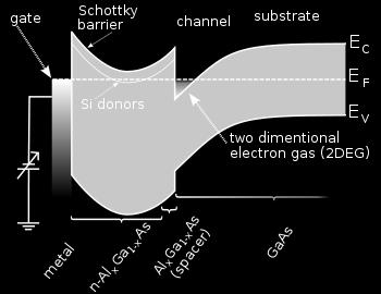
21 There are many theoretical models for the interface band alignment. However, the agreement between theory and experiments is often hampered by surface defects and imperfections, interface strains, etc. Still, the state-of-art technology can provide close-to-perfect interfaces, which can be considered by modern analytical and numerical models. Surfaces and Interfaces 21
22 Field effect transistors and quantum wells Si-MOSFET GaAs-HEMT Other devices Surfaces and Interfaces 22

23 Si-MOSFET p-doped Si Metallic gate Ohmic contacts Oxide, SiO 2 Band alignment along the dashed line at V g = 0 Surfaces and Interfaces 23
 Accumulation of holes Ambipolar device Surfaces and")
24 V g = 0 V g > 0 V g < 0 Inversion (acc. of electr.) Accumulation of holes Ambipolar device Surfaces and Interfaces 24


25 Wave functions and eigenenergies: Simple model Splitting of variables Triangular potential approximation Schrödinger equation Dimensionless variable Localization length Airy function Building blocks for nanodevices 25
26 Energy quantization is given by the roots Quasi 2DEG 2DEG Fermi level Each level generates a sub-band in the energy spectrum Building blocks for nanodevices 26

27 Transverse wave functions in a triangle well Normalized electron densities Building blocks for nanodevices 27
28 and Size quantization discrete modes! Quantized levels of transverse motion Electron density profile Quasi-two-dimensional electron gas Ions and electrons are separated and Coulomb scattering is relatively weak However, oxide is amorphous and the interface scattering is noticeable Surfaces and Interfaces 28
29 Usage of Si-MOSFETs for digital electronics according to CMOStechnology, as well as most important circuits for realizing logical operations are briefly discussed in the Sec of the textbook. Surfaces and Interfaces 29
 inside the Al 0.3 Ga 0.7 As. This is called the modulation doping. Surfaces and Interfaces 30")
30 GaAs-HEMT Typical choice interface Al 0.3 Ga 0.7 As - GaAs, Type I alignment, conduction band of Al 0.3 Ga 0.7 As is 300 mev higher than that one of GaAs. The top of the Al 0.3 Ga 0.7 As valence band is 160 mev below that of GaAs. In contrast to Si, GaAs remains undoped, and the electrons are provided by the doping layer (Si) inside the Al 0.3 Ga 0.7 As. This is called the modulation doping. Surfaces and Interfaces 30


31 Why δ-doping is advantageous? Scattering potential Doping layer 2DEG Matrix element Backscattering is exponentially suppressed large mobility Building blocks for nanodevices 31

32 Surfaces and Interfaces 32
33 Advantages of GaAs-based systems: Crystalline structure, low interface scattering; Doped layer is rather remote from the two-dimensional electron gas; Very high mobility: the present record is 1440 m 2 /Vs, that corresponds to the mean free path of 120 μm. Possibility to engineer band offsets by varying content of Al. In this way one can make quantum wells. Surfaces and Interfaces 33
34 Quantum confined vs. bulk carriers Evolution of electron mobility over time, after modulation doping was introduced After L. Pfeiffer et al., Surfaces and Interfaces 34


35 Significance of various scattering mechanisms in Ga[Al]As HEMT Dots experimental results for the structure with Surfaces and Interfaces 35

36 Many technological problems: lattice matching, interface states, possibilities for modulation doping, etc. doping of a heterostructure implemented in such way that the resulting free electrons are spatially separated from the positive donor ions; as a result scattering of moving electrons on the dopant atoms is avoided; aslo, due to the separation, electrons remain free and mobile even at the very low temperatures The band gap engineer s map It is shown which compounds can tolerate Building blocks for nanodevices 36
37 Other types of layered devices Quantum wells Surfaces and Interfaces 37

38 Organic FET pentacene Plastic transistors Less expensive Mechanically soft polythiophene At present time such systems are just in the beginning of the way Surfaces and Interfaces 38
39 Summary FETs and quantum well, and other layered devices are widely used. They are also promising for future. Interfaces strongly influence the band structure, in particular, dispersion laws, effective masses, etc. Many issues are already understood, but many things have to be done. Organic transistors are in the beginning of their way. Surfaces and Interfaces 39
Surfaces, Interfaces, and Layered Devices
 Surfaces, Interfaces, and Layered Devices Building blocks for nanodevices! W. Pauli: God made solids, but surfaces were the work of Devil. Surfaces and Interfaces 1 Role of surface effects in mesoscopic
Classification of Solids
 Classification of Solids Classification by conductivity, which is related to the band structure: (Filled bands are shown dark; D(E) = Density of states) Class Electron Density Density of States D(E) Examples
UNIVERSITY OF CALIFORNIA College of Engineering Department of Electrical Engineering and Computer Sciences. EECS 130 Professor Ali Javey Fall 2006
 UNIVERSITY OF CALIFORNIA College of Engineering Department of Electrical Engineering and Computer Sciences EECS 130 Professor Ali Javey Fall 2006 Midterm 2 Name: SID: Closed book. Two sheets of notes are
Current mechanisms Exam January 27, 2012
 Current mechanisms Exam January 27, 2012 There are four mechanisms that typically cause currents to flow: thermionic emission, diffusion, drift, and tunneling. Explain briefly which kind of current mechanisms
Figure 3.1 (p. 141) Figure 3.2 (p. 142)
 Figure 3.2 (p. 142)") Figure 3.1 (p. 141) Allowed electronic-energy-state systems for two isolated materials. States marked with an X are filled; those unmarked are empty. System 1 is a qualitative representation of a metal;
Figure 3.1 (p. 141) Allowed electronic-energy-state systems for two isolated materials. States marked with an X are filled; those unmarked are empty. System 1 is a qualitative representation of a metal;
EECS130 Integrated Circuit Devices
 EECS130 Integrated Circuit Devices Professor Ali Javey 10/02/2007 MS Junctions, Lecture 2 MOS Cap, Lecture 1 Reading: finish chapter14, start chapter16 Announcements Professor Javey will hold his OH at
Nanoscience and Molecular Engineering (ChemE 498A) Semiconductor Nano Devices
 Semiconductor Nano Devices") Reading: The first two readings cover the questions to bands and quasi-electrons/holes. See also problem 4. General Questions: 1. What is the main difference between a metal and a semiconductor or insulator,
Reading: The first two readings cover the questions to bands and quasi-electrons/holes. See also problem 4. General Questions: 1. What is the main difference between a metal and a semiconductor or insulator,
Final Examination EE 130 December 16, 1997 Time allotted: 180 minutes
 Final Examination EE 130 December 16, 1997 Time allotted: 180 minutes Problem 1: Semiconductor Fundamentals [30 points] A uniformly doped silicon sample of length 100µm and cross-sectional area 100µm 2
CME 300 Properties of Materials. ANSWERS: Homework 9 November 26, As atoms approach each other in the solid state the quantized energy states:
 CME 300 Properties of Materials ANSWERS: Homework 9 November 26, 2011 As atoms approach each other in the solid state the quantized energy states: are split. This splitting is associated with the wave
3. Two-dimensional systems
 3. Two-dimensional systems Image from IBM-Almaden 1 Introduction Type I: natural layered structures, e.g., graphite (with C nanostructures) Type II: artificial structures, heterojunctions Great technological
Semiconductor Physics fall 2012 problems
 Semiconductor Physics fall 2012 problems 1. An n-type sample of silicon has a uniform density N D = 10 16 atoms cm -3 of arsenic, and a p-type silicon sample has N A = 10 15 atoms cm -3 of boron. For each
Semiconductor Physics and Devices
 The pn Junction 1) Charge carriers crossing the junction. 3) Barrier potential Semiconductor Physics and Devices Chapter 8. The pn Junction Diode 2) Formation of positive and negative ions. 4) Formation
Review Energy Bands Carrier Density & Mobility Carrier Transport Generation and Recombination
 Review Energy Bands Carrier Density & Mobility Carrier Transport Generation and Recombination The Metal-Semiconductor Junction: Review Energy band diagram of the metal and the semiconductor before (a)
2.4 GaAs Heterostructures and 2D electron gas
 Semiconductor Surfaces and Interfaces 8 2.4 GaAs Heterostructures and 2D electron gas - To determine the band structure of the heterostructure, a self consistent solution of Poisson and Schrödinger equation
Lecture 2. Introduction to semiconductors Structures and characteristics in semiconductors
 Lecture 2 Introduction to semiconductors Structures and characteristics in semiconductors Semiconductor p-n junction Metal Oxide Silicon structure Semiconductor contact Literature Glen F. Knoll, Radiation
1 Name: Student number: DEPARTMENT OF PHYSICS AND PHYSICAL OCEANOGRAPHY MEMORIAL UNIVERSITY OF NEWFOUNDLAND. Fall :00-11:00
 1 Name: DEPARTMENT OF PHYSICS AND PHYSICAL OCEANOGRAPHY MEMORIAL UNIVERSITY OF NEWFOUNDLAND Final Exam Physics 3000 December 11, 2012 Fall 2012 9:00-11:00 INSTRUCTIONS: 1. Answer all seven (7) questions.
Avalanche breakdown. Impact ionization causes an avalanche of current. Occurs at low doping
 Avalanche breakdown Impact ionization causes an avalanche of current Occurs at low doping Zener tunneling Electrons tunnel from valence band to conduction band Occurs at high doping Tunneling wave decays
GaN based transistors
 GaN based transistors S FP FP dielectric G SiO 2 Al x Ga 1-x N barrier i-gan Buffer i-sic D Transistors "The Transistor was probably the most important invention of the 20th Century The American Institute
Semiconductor Module
 Semiconductor Module Optics Seminar July 18, 2018 Yosuke Mizuyama, Ph.D. COMSOL, Inc. The COMSOL Product Suite Governing Equations Semiconductor Schrödinger Equation Semiconductor Optoelectronics, FD Semiconductor
Chapter 3 Properties of Nanostructures
 Chapter 3 Properties of Nanostructures In Chapter 2, the reduction of the extent of a solid in one or more dimensions was shown to lead to a dramatic alteration of the overall behavior of the solids. Generally,
Semiconductor Physics fall 2012 problems
 Semiconductor Physics fall 2012 problems 1. An n-type sample of silicon has a uniform density N D = 10 16 atoms cm -3 of arsenic, and a p-type silicon sample has N A = 10 15 atoms cm -3 of boron. For each
* motif: a single or repeated design or color
 Chapter 2. Structure A. Electronic structure vs. Geometric structure B. Clean surface vs. Adsorbate covered surface (substrate + overlayer) C. Adsorbate structure - how are the adsorbed molecules bound
Lecture 9: Metal-semiconductor junctions
 Lecture 9: Metal-semiconductor junctions Contents 1 Introduction 1 2 Metal-metal junction 1 2.1 Thermocouples.......................... 2 3 Schottky junctions 4 3.1 Forward bias............................
Solid Surfaces, Interfaces and Thin Films
 Hans Lüth Solid Surfaces, Interfaces and Thin Films Fifth Edition With 427 Figures.2e Springer Contents 1 Surface and Interface Physics: Its Definition and Importance... 1 Panel I: Ultrahigh Vacuum (UHV)
Section 12: Intro to Devices
 Section 12: Intro to Devices Extensive reading materials on reserve, including Robert F. Pierret, Semiconductor Device Fundamentals Bond Model of Electrons and Holes Si Si Si Si Si Si Si Si Si Silicon
Lecture 2. Introduction to semiconductors Structures and characteristics in semiconductors
 Lecture 2 Introduction to semiconductors Structures and characteristics in semiconductors Semiconductor p-n junction Metal Oxide Silicon structure Semiconductor contact Literature Glen F. Knoll, Radiation
MOS CAPACITOR AND MOSFET
 EE336 Semiconductor Devices 1 MOS CAPACITOR AND MOSFET Dr. Mohammed M. Farag Ideal MOS Capacitor Semiconductor Devices Physics and Technology Chapter 5 EE336 Semiconductor Devices 2 MOS Capacitor Structure
Electron Energy, E E = 0. Free electron. 3s Band 2p Band Overlapping energy bands. 3p 3s 2p 2s. 2s Band. Electrons. 1s ATOM SOLID.
 Electron Energy, E Free electron Vacuum level 3p 3s 2p 2s 2s Band 3s Band 2p Band Overlapping energy bands Electrons E = 0 1s ATOM 1s SOLID In a metal the various energy bands overlap to give a single
Conductivity and Semi-Conductors
 Conductivity and Semi-Conductors J = current density = I/A E = Electric field intensity = V/l where l is the distance between two points Metals: Semiconductors: Many Polymers and Glasses 1 Electrical Conduction
Semiconductor Physics Problems 2015
 Semiconductor Physics Problems 2015 Page and figure numbers refer to Semiconductor Devices Physics and Technology, 3rd edition, by SM Sze and M-K Lee 1. The purest semiconductor crystals it is possible
Lecture 20: Semiconductor Structures Kittel Ch 17, p , extra material in the class notes
 Lecture 20: Semiconductor Structures Kittel Ch 17, p 494-503, 507-511 + extra material in the class notes MOS Structure Layer Structure metal Oxide insulator Semiconductor Semiconductor Large-gap Semiconductor
Schottky Rectifiers Zheng Yang (ERF 3017,
 ECE442 Power Semiconductor Devices and Integrated Circuits Schottky Rectifiers Zheng Yang (ERF 3017, email: yangzhen@uic.edu) Power Schottky Rectifier Structure 2 Metal-Semiconductor Contact The work function
R. Ludwig and G. Bogdanov RF Circuit Design: Theory and Applications 2 nd edition. Figures for Chapter 6
 R. Ludwig and G. Bogdanov RF Circuit Design: Theory and Applications 2 nd edition Figures for Chapter 6 Free electron Conduction band Hole W g W C Forbidden Band or Bandgap W V Electron energy Hole Valence
ET3034TUx Utilization of band gap energy
 ET3034TUx - 3.3.1 - Utilization of band gap energy In the last two weeks we have discussed the working principle of a solar cell and the external parameters that define the performance of a solar cell.
Schottky diodes. JFETs - MESFETs - MODFETs
 Technische Universität Graz Institute of Solid State Physics Schottky diodes JFETs - MESFETs - MODFETs Quasi Fermi level When the charge carriers are not in equilibrium the Fermi energy can be different
Lecture 1. OUTLINE Basic Semiconductor Physics. Reading: Chapter 2.1. Semiconductors Intrinsic (undoped) silicon Doping Carrier concentrations
 silicon Doping Carrier concentrations") Lecture 1 OUTLINE Basic Semiconductor Physics Semiconductors Intrinsic (undoped) silicon Doping Carrier concentrations Reading: Chapter 2.1 EE105 Fall 2007 Lecture 1, Slide 1 What is a Semiconductor? Low
Lecture 1 OUTLINE Basic Semiconductor Physics Semiconductors Intrinsic (undoped) silicon Doping Carrier concentrations Reading: Chapter 2.1 EE105 Fall 2007 Lecture 1, Slide 1 What is a Semiconductor? Low
Lecture 6 PN Junction and MOS Electrostatics(III) Metal-Oxide-Semiconductor Structure
 Metal-Oxide-Semiconductor Structure") Lecture 6 PN Junction and MOS Electrostatics(III) Metal-Oxide-Semiconductor Structure Outline 1. Introduction to MOS structure 2. Electrostatics of MOS in thermal equilibrium 3. Electrostatics of MOS with
Lecture 6 PN Junction and MOS Electrostatics(III) Metal-Oxide-Semiconductor Structure Outline 1. Introduction to MOS structure 2. Electrostatics of MOS in thermal equilibrium 3. Electrostatics of MOS with
Session 6: Solid State Physics. Diode
 Session 6: Solid State Physics Diode 1 Outline A B C D E F G H I J 2 Definitions / Assumptions Homojunction: the junction is between two regions of the same material Heterojunction: the junction is between
The discussion about p-n junctions in the semiconductor device is fundamental both
 CHAPTER II MATERIALS JUNCTIONS 2.1 p-n Junctions 2.1.1 Homojunction The discussion about p-n junctions in the semiconductor device is fundamental both in modern electronic applications and in understanding
Sheng S. Li. Semiconductor Physical Electronics. Second Edition. With 230 Figures. 4) Springer
 Springer") Sheng S. Li Semiconductor Physical Electronics Second Edition With 230 Figures 4) Springer Contents Preface 1. Classification of Solids and Crystal Structure 1 1.1 Introduction 1 1.2 The Bravais Lattice
Sheng S. Li Semiconductor Physical Electronics Second Edition With 230 Figures 4) Springer Contents Preface 1. Classification of Solids and Crystal Structure 1 1.1 Introduction 1 1.2 The Bravais Lattice
Nanoscience and Molecular Engineering (ChemE 498A) Semiconductor Nano Devices
 Semiconductor Nano Devices") Homework 7 Dec 9, 1 General Questions: 1 What is the main difference between a metal and a semiconductor or insulator, in terms of band structure? In a metal, the Fermi level (energy that separates full
Homework 7 Dec 9, 1 General Questions: 1 What is the main difference between a metal and a semiconductor or insulator, in terms of band structure? In a metal, the Fermi level (energy that separates full
Lecture 6: 2D FET Electrostatics
 Lecture 6: 2D FET Electrostatics 2016-02-01 Lecture 6, High Speed Devices 2014 1 Lecture 6: III-V FET DC I - MESFETs Reading Guide: Liu: 323-337 (he mainly focuses on the single heterostructure FET) Jena:
1. Binary III-V compounds 2 p From which atoms are the 16 binary III-V compounds formed?...column III B, Al, Ga and In...column V N, P, As and Sb...
 PROBLEMS part B, Semiconductor Materials. 2006 1. Binary III-V compounds 2 p From which atoms are the 16 binary III-V compounds formed?...column III B, Al, Ga and In...column V N, P, As and Sb... 2. Semiconductors
Lecture 04 Review of MOSFET
 ECE 541/ME 541 Microelectronic Fabrication Techniques Lecture 04 Review of MOSFET Zheng Yang (ERF 3017, email: yangzhen@uic.edu) What is a Transistor? A Switch! An MOS Transistor V GS V T V GS S Ron D
Lecture 2. Introduction to semiconductors Structures and characteristics in semiconductors. Fabrication of semiconductor sensor
 Lecture 2 Introduction to semiconductors Structures and characteristics in semiconductors Semiconductor p-n junction Metal Oxide Silicon structure Semiconductor contact Fabrication of semiconductor sensor
Semiconductor Junctions
 8 Semiconductor Junctions Almost all solar cells contain junctions between different materials of different doping. Since these junctions are crucial to the operation of the solar cell, we will discuss
Minimal Update of Solid State Physics
 Minimal Update of Solid State Physics It is expected that participants are acquainted with basics of solid state physics. Therefore here we will refresh only those aspects, which are absolutely necessary
PHYSICAL ELECTRONICS(ECE3540) CHAPTER 9 METAL SEMICONDUCTOR AND SEMICONDUCTOR HETERO-JUNCTIONS
 CHAPTER 9 METAL SEMICONDUCTOR AND SEMICONDUCTOR HETERO-JUNCTIONS") PHYSICAL ELECTRONICS(ECE3540) CHAPTER 9 METAL SEMICONDUCTOR AND SEMICONDUCTOR HETERO-JUNCTIONS Tennessee Technological University Monday, November 11, 013 1 Introduction Chapter 4: we considered the semiconductor
PHYSICAL ELECTRONICS(ECE3540) CHAPTER 9 METAL SEMICONDUCTOR AND SEMICONDUCTOR HETERO-JUNCTIONS Tennessee Technological University Monday, November 11, 013 1 Introduction Chapter 4: we considered the semiconductor
Typical example of the FET: MEtal Semiconductor FET (MESFET)
") Typical example of the FET: MEtal Semiconductor FET (MESFET) Conducting channel (RED) is made of highly doped material. The electron concentration in the channel n = the donor impurity concentration N
Typical example of the FET: MEtal Semiconductor FET (MESFET) Conducting channel (RED) is made of highly doped material. The electron concentration in the channel n = the donor impurity concentration N
Semiconductor Physical Electronics
 Semiconductor Physical Electronics Sheng S. Li Department of Electrical Engineering University of Florida Gainesville, Florida Plenum Press New York and London Contents CHAPTER 1. Classification of Solids
PHYSICAL ELECTRONICS(ECE3540) CHAPTER 9 METAL SEMICONDUCTOR AND SEMICONDUCTOR HETERO-JUNCTIONS
 CHAPTER 9 METAL SEMICONDUCTOR AND SEMICONDUCTOR HETERO-JUNCTIONS") PHYSICAL ELECTRONICS(ECE3540) CHAPTER 9 METAL SEMICONDUCTOR AND SEMICONDUCTOR HETERO-JUNCTIONS Tennessee Technological University Wednesday, October 30, 013 1 Introduction Chapter 4: we considered the
PHYSICAL ELECTRONICS(ECE3540) CHAPTER 9 METAL SEMICONDUCTOR AND SEMICONDUCTOR HETERO-JUNCTIONS Tennessee Technological University Wednesday, October 30, 013 1 Introduction Chapter 4: we considered the
Introduction to Semiconductor Physics. Prof.P. Ravindran, Department of Physics, Central University of Tamil Nadu, India
 Introduction to Semiconductor Physics 1 Prof.P. Ravindran, Department of Physics, Central University of Tamil Nadu, India http://folk.uio.no/ravi/cmp2013 Review of Semiconductor Physics Semiconductor fundamentals
KATIHAL FİZİĞİ MNT-510
 KATIHAL FİZİĞİ MNT-510 YARIİLETKENLER Kaynaklar: Katıhal Fiziği, Prof. Dr. Mustafa Dikici, Seçkin Yayıncılık Katıhal Fiziği, Şakir Aydoğan, Nobel Yayıncılık, Physics for Computer Science Students: With
Semiconductor device structures are traditionally divided into homojunction devices
 0. Introduction: Semiconductor device structures are traditionally divided into homojunction devices (devices consisting of only one type of semiconductor material) and heterojunction devices (consisting
Quantum Phenomena & Nanotechnology (4B5)
") Quantum Phenomena & Nanotechnology (4B5) The 2-dimensional electron gas (2DEG), Resonant Tunneling diodes, Hot electron transistors Lecture 11 In this lecture, we are going to look at 2-dimensional electron
Quantum Phenomena & Nanotechnology (4B5) The 2-dimensional electron gas (2DEG), Resonant Tunneling diodes, Hot electron transistors Lecture 11 In this lecture, we are going to look at 2-dimensional electron
Effective masses in semiconductors
 Effective masses in semiconductors The effective mass is defined as: In a solid, the electron (hole) effective mass represents how electrons move in an applied field. The effective mass reflects the inverse
ECE 340 Lecture 27 : Junction Capacitance Class Outline:
 ECE 340 Lecture 27 : Junction Capacitance Class Outline: Breakdown Review Junction Capacitance Things you should know when you leave M.J. Gilbert ECE 340 Lecture 27 10/24/11 Key Questions What types of
8. Schottky contacts / JFETs
 Technische Universität Graz Institute of Solid State Physics 8. Schottky contacts / JFETs Nov. 21, 2018 Technische Universität Graz Institute of Solid State Physics metal - semiconductor contacts Photoelectric
Review of Semiconductor Physics
 Solid-state physics Review of Semiconductor Physics The daunting task of solid state physics Quantum mechanics gives us the fundamental equation The equation is only analytically solvable for a handful
LEC E T C U T R U E R E 17 -Photodetectors
 LECTURE 17 -Photodetectors Topics to be covered Photodetectors PIN photodiode Avalanche Photodiode Photodetectors Principle of the p-n junction Photodiode A generic photodiode. Photodetectors Principle
Solid State Electronics. Final Examination
 The University of Toledo EECS:4400/5400/7400 Solid State Electronic Section elssf08fs.fm - 1 Solid State Electronics Final Examination Problems Points 1. 1. 14 3. 14 Total 40 Was the exam fair? yes no
Appendix 1: List of symbols
 Appendix 1: List of symbols Symbol Description MKS Units a Acceleration m/s 2 a 0 Bohr radius m A Area m 2 A* Richardson constant m/s A C Collector area m 2 A E Emitter area m 2 b Bimolecular recombination
Chap. 11 Semiconductor Diodes
 Chap. 11 Semiconductor Diodes Semiconductor diodes provide the best resolution for energy measurements, silicon based devices are generally used for charged-particles, germanium for photons. Scintillators
Calculating Band Structure
 Calculating Band Structure Nearly free electron Assume plane wave solution for electrons Weak potential V(x) Brillouin zone edge Tight binding method Electrons in local atomic states (bound states) Interatomic
2) Atom manipulation. Xe / Ni(110) Model: Experiment:
 Atom manipulation. Xe / Ni(110) Model: Experiment:") 2) Atom manipulation D. Eigler & E. Schweizer, Nature 344, 524 (1990) Xe / Ni(110) Model: Experiment: G.Meyer, et al. Applied Physics A 68, 125 (1999) First the tip is approached close to the adsorbate
2) Atom manipulation D. Eigler & E. Schweizer, Nature 344, 524 (1990) Xe / Ni(110) Model: Experiment: G.Meyer, et al. Applied Physics A 68, 125 (1999) First the tip is approached close to the adsorbate
FREQUENTLY ASKED QUESTIONS February 21, 2017
 FREQUENTLY ASKED QUESTIONS February 21, 2017 Content Questions How do you place a single arsenic atom with the ratio 1 in 100 million? Sounds difficult to get evenly spread throughout. Yes, techniques
MSE 310/ECE 340: Electrical Properties of Materials Fall 2014 Department of Materials Science and Engineering Boise State University
 MSE 310/ECE 340: Electrical Properties of Materials Fall 2014 Department of Materials Science and Engineering Boise State University Practice Final Exam 1 Read the questions carefully Label all figures
Metal Semiconductor Contacts
 Metal Semiconductor Contacts The investigation of rectification in metal-semiconductor contacts was first described by Braun [33-35], who discovered in 1874 the asymmetric nature of electrical conduction
Band Alignment and Graded Heterostructures. Guofu Niu Auburn University
 Band Alignment and Graded Heterostructures Guofu Niu Auburn University Outline Concept of electron affinity Types of heterojunction band alignment Band alignment in strained SiGe/Si Cusps and Notches at
UNIVERSITY OF CALIFORNIA College of Engineering Department of Electrical Engineering and Computer Sciences. EECS 130 Professor Ali Javey Fall 2006
 UNIVERSITY OF CALIFORNIA College of Engineering Department of Electrical Engineering and Computer Sciences EECS 130 Professor Ali Javey Fall 2006 Midterm I Name: Closed book. One sheet of notes is allowed.
Chapter 4: Bonding in Solids and Electronic Properties. Free electron theory
 Chapter 4: Bonding in Solids and Electronic Properties Free electron theory Consider free electrons in a metal an electron gas. regards a metal as a box in which electrons are free to move. assumes nuclei
Introduction to Power Semiconductor Devices
 ECE442 Power Semiconductor Devices and Integrated Circuits Introduction to Power Semiconductor Devices Zheng Yang (ERF 3017, email: yangzhen@uic.edu) Power Semiconductor Devices Applications System Ratings
Module-6: Schottky barrier capacitance-impurity concentration
 6.1 Introduction: Module-6: Schottky barrier capacitance-impurity concentration The electric current flowing across a metal semiconductor interface is generally non-linear with respect to the applied bias
Semiconductors. Semiconductors also can collect and generate photons, so they are important in optoelectronic or photonic applications.
 Semiconductors Semiconducting materials have electrical properties that fall between true conductors, (like metals) which are always highly conducting and insulators (like glass or plastic or common ceramics)
V BI. H. Föll: kiel.de/matwis/amat/semi_en/kap_2/backbone/r2_2_4.html. different electrochemical potentials (i.e.
 Consider the the band diagram for a homojunction, formed when two bits of the same type of semicondutor (e.g. Si) are doped p and ntype and then brought into contact. Electrons in the two bits have different
MOS Capacitor MOSFET Devices. MOSFET s. INEL Solid State Electronics. Manuel Toledo Quiñones. ECE Dept. UPRM.
 INEL 6055 - Solid State Electronics ECE Dept. UPRM 20th March 2006 Definitions MOS Capacitor Isolated Metal, SiO 2, Si Threshold Voltage qφ m metal d vacuum level SiO qχ 2 E g /2 qφ F E C E i E F E v qφ
Chemistry Instrumental Analysis Lecture 8. Chem 4631
 Chemistry 4631 Instrumental Analysis Lecture 8 UV to IR Components of Optical Basic components of spectroscopic instruments: stable source of radiant energy transparent container to hold sample device
an introduction to Semiconductor Devices
 an introduction to Semiconductor Devices Donald A. Neamen Chapter 6 Fundamentals of the Metal-Oxide-Semiconductor Field-Effect Transistor Introduction: Chapter 6 1. MOSFET Structure 2. MOS Capacitor -
Consider a uniformly doped PN junction, in which one region of the semiconductor is uniformly doped with acceptor atoms and the adjacent region is
 CHAPTER 7 The PN Junction Consider a uniformly doped PN junction, in which one region of the semiconductor is uniformly doped with acceptor atoms and the adjacent region is uniformly doped with donor atoms.
Electrostatics of Nanowire Transistors
 Electrostatics of Nanowire Transistors Jing Guo, Jing Wang, Eric Polizzi, Supriyo Datta and Mark Lundstrom School of Electrical and Computer Engineering Purdue University, West Lafayette, IN, 47907 ABSTRACTS
EE143 Fall 2016 Microfabrication Technologies. Evolution of Devices
 EE143 Fall 2016 Microfabrication Technologies Prof. Ming C. Wu wu@eecs.berkeley.edu 511 Sutardja Dai Hall (SDH) 1-1 Evolution of Devices Yesterday s Transistor (1947) Today s Transistor (2006) 1-2 1 Why
Semiconductor Detectors are Ionization Chambers. Detection volume with electric field Energy deposited positive and negative charge pairs
 1 V. Semiconductor Detectors V.1. Principles Semiconductor Detectors are Ionization Chambers Detection volume with electric field Energy deposited positive and negative charge pairs Charges move in field
Laser Diodes. Revised: 3/14/14 14: , Henry Zmuda Set 6a Laser Diodes 1
 Laser Diodes Revised: 3/14/14 14:03 2014, Henry Zmuda Set 6a Laser Diodes 1 Semiconductor Lasers The simplest laser of all. 2014, Henry Zmuda Set 6a Laser Diodes 2 Semiconductor Lasers 1. Homojunction
Lecture 12: MOS Capacitors, transistors. Context
 Lecture 12: MOS Capacitors, transistors Context In the last lecture, we discussed PN diodes, and the depletion layer into semiconductor surfaces. Small signal models In this lecture, we will apply those
Electronics The basics of semiconductor physics
 Electronics The basics of semiconductor physics Prof. Márta Rencz, Gergely Nagy BME DED September 16, 2013 The basic properties of semiconductors Semiconductors conductance is between that of conductors
Introductory Nanotechnology ~ Basic Condensed Matter Physics ~
 Introductory Nanotechnology ~ Basic Condensed Matter Physics ~ Atsufumi Hirohata Department of Electronics Quick Review over the Last Lecture Classic model : Dulong-Petit empirical law c V, mol 3R 0 E
PN Junction
 P Junction 2017-05-04 Definition Power Electronics = semiconductor switches are used Analogue amplifier = high power loss 250 200 u x 150 100 u Udc i 50 0 0 50 100 150 200 250 300 350 400 i,u dc i,u u
Choice of V t and Gate Doping Type
 Choice of V t and Gate Doping Type To make circuit design easier, it is routine to set V t at a small positive value, e.g., 0.4 V, so that, at V g = 0, the transistor does not have an inversion layer and
Basic cell design. Si cell
 Basic cell design Si cell 1 Concepts needed to describe photovoltaic device 1. energy bands in semiconductors: from bonds to bands 2. free carriers: holes and electrons, doping 3. electron and hole current:
ECE236A Semiconductor Heterostructure Materials Basic Properties of Semiconductor Heterostructures Lectures 2 & 3 Oct. 5, 2017
 ECE236A Semiconductor Heterostructure Materials Basic Properties of Semiconductor Heterostructures Lectures 2 & 3 Oct. 5, 217 Basic definitions. Types of band-alignment. Determination of band-offsets:
Band diagrams of heterostructures
 Herbert Kroemer (1928) 17 Band diagrams of heterostructures 17.1 Band diagram lineups In a semiconductor heterostructure, two different semiconductors are brought into physical contact. In practice, different
ECE 340 Lecture 35 : Metal- Semiconductor Junctions Class Outline:
 ECE 340 Lecture 35 : - Junctions Class Outline: Ideal - Contacts Rectifying Contacts Ohmic Contacts Things you should know when you leave Key Questions What happens to the bands when we make contact between
Semiconductor Devices and Circuits Fall Midterm Exam. Instructor: Dr. Dietmar Knipp, Professor of Electrical Engineering. Name: Mat. -Nr.
 Semiconductor Devices and Circuits Fall 2003 Midterm Exam Instructor: Dr. Dietmar Knipp, Professor of Electrical Engineering Name: Mat. -Nr.: Guidelines: Duration of the Midterm: 1 hour The exam is a closed
Fundamentals of the Metal Oxide Semiconductor Field-Effect Transistor
 Triode Working FET Fundamentals of the Metal Oxide Semiconductor Field-Effect Transistor The characteristics of energy bands as a function of applied voltage. Surface inversion. The expression for the
CLASS 12th. Semiconductors
 CLASS 12th Semiconductors 01. Distinction Between Metals, Insulators and Semi-Conductors Metals are good conductors of electricity, insulators do not conduct electricity, while the semiconductors have
Peak Electric Field. Junction breakdown occurs when the peak electric field in the PN junction reaches a critical value. For the N + P junction,
 Peak Electric Field Junction breakdown occurs when the peak electric field in the P junction reaches a critical value. For the + P junction, qa E ( x) ( xp x), s W dep 2 s ( bi Vr ) 2 s potential barrier
Spring Semester 2012 Final Exam
 Spring Semester 2012 Final Exam Note: Show your work, underline results, and always show units. Official exam time: 2.0 hours; an extension of at least 1.0 hour will be granted to anyone. Materials parameters
Lecture 7: Extrinsic semiconductors - Fermi level
 Lecture 7: Extrinsic semiconductors - Fermi level Contents 1 Dopant materials 1 2 E F in extrinsic semiconductors 5 3 Temperature dependence of carrier concentration 6 3.1 Low temperature regime (T < T
Thermionic Emission Theory
 hapter 4. PN and Metal-Semiconductor Junction Thermionic Emiion Theory Energy band diagram of a Schottky contact with a forward bia V applied between the metal and the emiconductor. Electron concentration
ECEN 3320 Semiconductor Devices Final exam - Sunday December 17, 2000
 Your Name: ECEN 3320 Semiconductor Devices Final exam - Sunday December 17, 2000 1. Review questions a) Illustrate the generation of a photocurrent in a p-n diode by drawing an energy band diagram. Indicate