The Prospects for III-Vs
|
|
|
- Tobias Lawson
- 5 years ago
- Views:
Transcription


1 10 nm CMOS: The Prospects for III-Vs J. A. del Alamo, Dae-Hyun Kim 1, Donghyun Jin, and Taewoo Kim Microsystems Technology Laboratories, MIT 1 Presently with Teledyne Scientific 2010 European Materials Research Society Spring Meeting June 7-10, 2010 Sponsors: Intel, FCRP-MSD Acknowledgements: Niamh Waldron, Ling Xia, Dimitri Antoniadis, Robert Chau MTL, NSL, SEBL 1
2 Outline Introduction: Why III-Vs for CMOS? What have we learned from III-V HEMTs? What are the challenges for III-V CMOS? The prospects of 10 nm III-V CMOS Conclusions 2
3 Why III-Vs for CMOS? Si CMOS has entered era of power-constrained scaling : CPU power density saturated at ~100 W/cm 2 CPU clock speed saturated at ~ 4 GHz ca/ nlipkowi/pictures/clo Pop, Nano Res 2010 ckspeeds.gif 3
4 Why III-Vs for CMOS? Under power-constrained scaling: Power = active power + passive power #1 goal ~ fcv DD2 N N N V DD But, V DD scaling very weakly: V DD 4 Chen, IEDM
5 Why III-Vs for CMOS? Need scaling approach that allows V DD reduction Goal of scaling: reduce footprint extract maximum I ON for given I OFF III-Vs: Much higher injection velocity than Si I ON Very tight carrier confinement possible S 5
6 III-V CMOS: What are the challenges? To know where you are going, you first have to know where you are. We are starting from: III-V High Electron Mobility Transistors 6
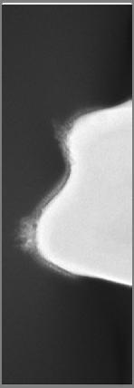

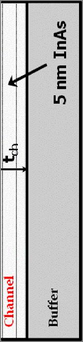
7 III-V HEMTs State-of-the-art: InAs-channel HEMT - QW channel (t ch = 10 nm) : - InAs core (t InAs = 5 nm) - InGaAs cladding - n,hall = 13,200 cm 2 /V-sec - InAlAs barrier (t ins = 4 nm) - Two-step recess - Pt/Ti/Mo/Au Schottky gate Kim, IEDM L g =30 nm 7
8 III-V HEMTs L g =30 nm InAs-channel HEMT Kim, IEDM V GS = 0.5 V I D [ma/ m m] 0.4 V GS = 04V 0.4 g m [ms/ m] V DS [V] V DS = 0.5 V V GS - V T [V] Large current drive: I on =0.4 ma/µm at V DD =0.5 V Enhancement-mode FET: V T = 0.08 V High transconductance: g mpk = 1.8 ms/um at V DD =0.5 V 8
9 III-V HEMTs L g =30 nm InAs-channel HEMT Kim, IEDM 2008 I D, I G [A/ m] =05V 10-7 V 0.5 DS V DS = 0.05 V I D V GS [V] I G H 21, U g, MAG [d db] H 21 U g MAG f T =601 GHz f max =609 GHz V = 0.5 V, V = 0.3 V DS GS Frequency [GHz] S = 73 mv/dec, DIBL = 85 mv/v, I on /I off =~10 4 First transistor with both f T and f max > 600 GHz 9
10 Scaling of III-V HEMTs: Benchmarking with Si Sub bthreshold sw wing [mv/dec.] 180 Si FETs (IEDM)* Triple recess: IEDM Pt sinking: IEDM iedm Gate Length [nm] iedm06 iedm07 AY [psec] GATE DEL 10 1 Si NMOSFETs iedm Gate Length, L g [nm] iedm06 iedm07 InAs HEMTs (V CC = 0.5V) (V CC = 1.1~1.3V) V DD =0.5 V Superior short-channel effects as compared to Si MOSFETs Lower gate delay than Si MOSFETs at lower V DD 10
11 Scaling of III-V HEMTs: Benchmarking with Si I I OFF =100 na/µm, V DD =0.5 V: FOM that integrates short-channel effects and drive current (scaled to V DD =0.5 V) III-V HEMTs: higher I ON for same I OFF than Si 11

 )increases with ithinas fraction in channel v inj (InGaAs) >")
12 What can we learn from III-V HEMTs? 1. Very high electron injection velocity at the virtual source Kim, IEDM 2009 E C v inj 0 L x v in nj v inj electron injection velocity at virtual source v inj (InGaAs) )increases with ithinas fraction in channel v inj (InGaAs) > 2v inj (Si) at less than half V DD 12
13 What can we learn from III-V HEMTs? 2. Quantum-well channel key to outstanding short-channel effects Kim, IPRM 2010 Dramatic improvement in electrostatic t ti integrity it in thin channel devices 13

 InAs channel t ch =")
![10 nm Experiment (C G ) Capacitance [ff F/ m 2 ] 30 20 10 C ins ( t](/docs-images/87/96606804/images/14-2.jpg "ins = 4 nm) 30 C Q1 Capacitance [ff F/ m 2 ] 20 CG C cent1 10 C ins (")
 0-0.4-0.2 0")
14 What can we learn from III-V HEMTs? 3. Quantum capacitance less of a bottleneck than commonly believed In 0.7 Ga 0.3 As channel t ch = 13 nm Experiment (C G ) InAs channel t ch = 10 nm Experiment (C G ) Capacitance [ff F/ m 2 ] C ins ( t ins = 4 nm) 30 C Q1 Capacitance [ff F/ m 2 ] 20 CG C cent1 10 C ins ( t ins = 4 nm) C Q1 (m * = 0.026m e ) C cent1 C G ( 0.07 ) C G (005) 0.05 C G (m * = 0.026m e ) V G [V] V G [V] G Biaxial strain + non-parabolicity + strong quantization increase m * C G Jin, IEDM
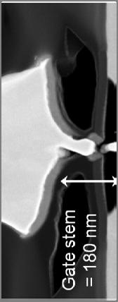
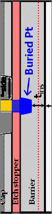
15 Limit to III-V HEMT Scaling: Gate Leakage age Current InAs HEMT 10-3 t ins = 10 nm L g =30nm t ins =7nm t ins = 4 nm t ch = 10 nm I D, I [A/ m] D G I D t ins =4 nm t ins =7nm t ins I G 10-9 t ins =10 nm DS V DS = 0.5 V V GS [V] t ins I G Further scaling requires high-k gate dielectric 15


16 The Challenges for III-V CMOS: III-V HEMT vs. Si CMOS III-V HEMT Intel s 45 nm CMOS Critical issues: Schottky gate MOS gate Footprint scaling [1000x too big!] Need self-aligned contacts Need p-channel device Need III-V on Si 16
17 The High-K/III-V System by ALD Ex-situ ALD produces high-quality interface on InGaAs: Surface inversion demonstrated Al 2 O 3 /In 0.52 Ga 0.47 As D it in mid ~10 11 cm -2.eV -1 demonstrated Al 2 O 3 /In 0.52 Ga 0.47 As f=100 Hz-1 MHz 2.40E-011 Al 2 O 3 /In 0.65 Ga 0.35 As In 0.65 Ga 0.35 As MOS-Cap C gb on D=75um Lin, SISC 2008 Capacitance (F) 2.00E E E-011 f T ~55.56KHz 8.00E-012 Ye, E Bias (V) 17
18 In 0.7 Ga 0.3 As Quantum-Well MOSFET Direct MBE on Si substrate (1.5 µm buffer thickness) InGaAs buried-channel MOSFET (under 2 nm InP etch stop) 4 nm TaSiO x gate dielectric by ALD, TiN/Pt/Au gate L g =75 nm Radosavljevic, IEDM
19 In 0.7 Ga 0.3 As Quantum-Well MOSFET (scaled to V DD =0.5 V) 2009 Intel InGaAs MOSFET 19

20 What can we expect from ~10 nm III-V NMOS at 0.5 V? With thin InAs channel: Assume R S as in Si (~80 Ω.µm): S Key requirements: I D =1.5 ma/µm Three greatest worries! High-K/III-V interface, thin channel do not degrade v inj Obtaining R s =80 Ω.µm at required footprint Acceptable short-channel effects 20
21 Conclusions III-Vs attractive for CMOS: key for low V DD operation Electron injection velocity in InAs > 2X that of Si at 1/2X V DD Quantum well channel yields outstanding short-channel effects Quantum capacitance less of a limitation than previously believed Impressive recent progress on III-V CMOS Ex-situ ALD and MOCVD on InGaAs yield interfaces with unpinned Fermi level and low defect density Sub-100 nm InGaAs MOSFETs with I ON > than Si at 0.5 V demonstrated Lots of work ahead: Demonstrate 10 nm III-V MOSFET that is better than Si P-channel MOSFET Manufacturability, reliability 21
III-V CMOS: What have we learned from HEMTs? J. A. del Alamo, D.-H. Kim 1, T.-W. Kim, D. Jin, and D. A. Antoniadis
 III-V CMOS: What have we learned from HEMTs? J. A. del Alamo, D.-H. Kim 1, T.-W. Kim, D. Jin, and D. A. Antoniadis Microsystems Technology Laboratories, MIT 1 presently with Teledyne Scientific 23rd International
30 nm In 0.7 Ga 0.3 As Inverted-type HEMT with Reduced Gate Leakage Current for Logic Applications
 30 nm In 0.7 Ga 0.3 As Inverted-type HEMT with Reduced Gate Leakage Current for Logic Applications T.-W. Kim, D.-H. Kim* and J. A. del Alamo Microsystems Technology Laboratories MIT Presently with Teledyne
Microsystems Technology Laboratories, MIT. Teledyne Scientific Company (TSC)
") Extraction of Virtual-Source Injection Velocity in sub-100 nm III-V HFETs 1,2) D.-H. Kim, 1) J. A. del Alamo, 1) D. A. Antoniadis and 2) B. Brar 1) Microsystems Technology Laboratories, MIT 2) Teledyne
Extraction of Virtual-Source Injection Velocity in sub-100 nm III-V HFETs 1,2) D.-H. Kim, 1) J. A. del Alamo, 1) D. A. Antoniadis and 2) B. Brar 1) Microsystems Technology Laboratories, MIT 2) Teledyne
Ultra-Scaled InAs HEMTs
 Performance Analysis of Ultra-Scaled InAs HEMTs Neerav Kharche 1, Gerhard Klimeck 1, Dae-Hyun Kim 2,3, Jesús. A. del Alamo 2, and Mathieu Luisier 1 1 Network for Computational ti Nanotechnology and Birck
Performance Analysis of Ultra-Scaled InAs HEMTs
 Purdue University Purdue e-pubs Birck and NCN Publications Birck Nanotechnology Center 2009 Performance Analysis of Ultra-Scaled InAs HEMTs Neerav Kharche Birck Nanotechnology Center and Purdue University,
Performance Enhancement of P-channel InGaAs Quantum-well FETs by Superposition of Process-induced Uniaxial Strain and Epitaxially-grown Biaxial Strain
 Performance Enhancement of P-channel InGaAs Quantum-well FETs by Superposition of Process-induced Uniaxial Strain and Epitaxially-grown Biaxial Strain Ling Xia 1, Vadim Tokranov 2, Serge R. Oktyabrsky
Quantum-size effects in sub-10 nm fin width InGaAs finfets
 Quantum-size effects in sub-10 nm fin width InGaAs finfets Alon Vardi, Xin Zhao, and Jesús A. del Alamo Microsystems Technology Laboratories, MIT December 9, 2015 Sponsors: DTRA NSF (E3S STC) Northrop
Self-Aligned InGaAs FinFETs with 5-nm Fin-Width and 5-nm Gate-Contact Separation
 Self-Aligned InGaAs FinFETs with 5-nm Fin-Width and 5-nm Gate-Contact Separation Alon Vardi, Lisa Kong, Wenjie Lu, Xiaowei Cai, Xin Zhao, Jesús Grajal* and Jesús A. del Alamo Microsystems Technology Laboratories,
Comparison of Ultra-Thin InAs and InGaAs Quantum Wells and Ultra-Thin-Body Surface-Channel MOSFETs
 Comparison of Ultra-Thin InAs and InGaAs Quantum Wells and Ultra-Thin-Body Surface-Channel MOSFETs Cheng-Ying Huang 1, Sanghoon Lee 1, Evan Wilson 3, Pengyu Long 3, Michael Povolotskyi 3, Varistha Chobpattana
Components Research, TMG Intel Corporation *QinetiQ. Contact:
 1 High-Performance 4nm Gate Length InSb P-Channel Compressively Strained Quantum Well Field Effect Transistors for Low-Power (V CC =.5V) Logic Applications M. Radosavljevic,, T. Ashley*, A. Andreev*, S.
Electric-Field Induced F - Migration in Self-Aligned InGaAs MOSFETs and Mitigation
 Electric-Field Induced F - Migration in Self-Aligned InGaAs MOSFETs and Mitigation X. Cai, J. Lin, D. A. Antoniadis and J. A. del Alamo Microsystems Technology Laboratories, MIT December 5, 2016 Sponsors:
High Mobility Materials and Novel Device Structures for High Performance Nanoscale MOSFETs
 High Mobility Materials and Novel Device Structures for High Performance Nanoscale MOSFETs Prof. (Dr.) Tejas Krishnamohan Department of Electrical Engineering Stanford University, CA & Intel Corporation
Prospects for Ge MOSFETs
 Prospects for Ge MOSFETs Sematech Workshop December 4, 2005 Dimitri A. Antoniadis Microsystems Technology Laboratories MIT Sematech Workshop 2005 1 Channel Transport - I D I D =WQ i (x 0 )v xo v xo : carrier
InGaAs Double-Gate Fin-Sidewall MOSFET
 InGaAs Double-Gate Fin-Sidewall MOSFET Alon Vardi, Xin Zhao and Jesús del Alamo Microsystems Technology Laboratories, MIT June 25, 214 Sponsors: Sematech, Technion-MIT Fellowship, and NSF E3S Center (#939514)
High aspect-ratio InGaAs FinFETs with sub-20 nm fin width
 High aspect-rati InGaAs FinFETs with sub-2 nm fin width Aln Vardi, Jianqiang Lin, Wenjie Lu, Xin Zha and Jesús A. del Alam Micrsystems Technlgy Labratries, MIT June 15, 216 Spnsrs: DTRA (HDTRA 1-14-1-57),
Technology Development & Design for 22 nm InGaAs/InP-channel MOSFETs
 2008 Indium Phosphide and Related Materials Conference, May, Versailles, France Technology Development & Design for 22 nm InGaAs/InP-channel MOSFETs M. Rodwell University of California, Santa Barbara M.
Technology Development for InGaAs/InP-channel MOSFETs
 MRS Spring Symposium, Tutorial: Advanced CMOS Substrates, Devices, Reliability, and Characterization, April 13, 2009, San Francisco Technology Development for InGaAs/InP-channel MOSFETs Mark Rodwell University
Negative-Bias Temperature Instability (NBTI) of GaN MOSFETs
 of GaN MOSFETs") Negative-Bias Temperature Instability (NBTI) of GaN MOSFETs Alex Guo and Jesús A. del Alamo Microsystems Technology Laboratories (MTL) Massachusetts Institute of Technology (MIT) Cambridge, MA, USA Sponsor:
Negative-Bias Temperature Instability (NBTI) of GaN MOSFETs Alex Guo and Jesús A. del Alamo Microsystems Technology Laboratories (MTL) Massachusetts Institute of Technology (MIT) Cambridge, MA, USA Sponsor:
Analysis of Band-to-band. Tunneling Structures. Title of Talk. Dimitri Antoniadis and Judy Hoyt (PIs) Jamie Teherani and Tao Yu (Students) 8/21/2012
 Jamie Teherani and Tao Yu (Students) 8/21/2012") 1 Analysis of Band-to-band Title of Talk Tunneling Structures Dimitri Antoniadis and Judy Hoyt (PIs) Jamie Teherani and Tao Yu (Students) 8/21/2012 A Science & Technology Center Vertical Type-II TFET Structure
1 Analysis of Band-to-band Title of Talk Tunneling Structures Dimitri Antoniadis and Judy Hoyt (PIs) Jamie Teherani and Tao Yu (Students) 8/21/2012 A Science & Technology Center Vertical Type-II TFET Structure
Simple Theory of the Ballistic Nanotransistor
 Simple Theory of the Ballistic Nanotransistor Mark Lundstrom Purdue University Network for Computational Nanoechnology outline I) Traditional MOS theory II) A bottom-up approach III) The ballistic nanotransistor
The Pennsylvania State University. Kurt J. Lesker Company. North Carolina State University. Taiwan Semiconductor Manufacturing Company 1
 Enhancement Mode Strained (1.3%) Germanium Quantum Well FinFET (W fin =20nm) with High Mobility (μ Hole =700 cm 2 /Vs), Low EOT (~0.7nm) on Bulk Silicon Substrate A. Agrawal 1, M. Barth 1, G. B. Rayner
Carbon Nanotube Electronics
 Carbon Nanotube Electronics Jeorg Appenzeller, Phaedon Avouris, Vincent Derycke, Stefan Heinz, Richard Martel, Marko Radosavljevic, Jerry Tersoff, Shalom Wind H.-S. Philip Wong hspwong@us.ibm.com IBM T.J.
Electrical Degradation of InAlAs/InGaAs Metamorphic High-Electron Mobility Transistors
 Electrical Degradation of InAlAs/InGaAs Metamorphic High-Electron Mobility Transistors S. D. Mertens and J.A. del Alamo Massachusetts Institute of Technology Sponsor: Agilent Technologies Outline Introduction
Impact of 110 uniaxial strain on n-channel In0.15Ga0.85As high electron mobility transistors
 Impact of 110 uniaxial strain on n-channel In0.15Ga0.85As high electron mobility transistors The MIT Faculty has made this article openly available. Please share how this access benefits you. Your story
OFF-state TDDB in High-Voltage GaN MIS-HEMTs
 OFF-state TDDB in High-Voltage GaN MIS-HEMTs Shireen Warnock and Jesús A. del Alamo Microsystems Technology Laboratories (MTL) Massachusetts Institute of Technology (MIT) Purpose Further understanding
Time Dependent Dielectric Breakdown in High Voltage GaN MIS HEMTs: The Role of Temperature
 Time Dependent Dielectric Breakdown in High Voltage GaN MIS HEMTs: The Role of Temperature Shireen Warnock, Allison Lemus, and Jesús A. del Alamo Microsystems Technology Laboratories (MTL) Massachusetts
ALD high-k and higher-k integration on GaAs
 ALD high-k and higher-k integration on GaAs Ozhan Koybasi 1), Min Xu 1), Yiqun Liu 2), Jun-Jieh Wang 2), Roy G. Gordon 2), and Peide D. Ye 1)* 1) School of Electrical and Computer Engineering, Purdue University,
CMPEN 411 VLSI Digital Circuits. Lecture 03: MOS Transistor
 CMPEN 411 VLSI Digital Circuits Lecture 03: MOS Transistor Kyusun Choi [Adapted from Rabaey s Digital Integrated Circuits, Second Edition, 2003 J. Rabaey, A. Chandrakasan, B. Nikolic] CMPEN 411 L03 S.1
III V compound semiconductors have recently emerged as
 1504 IEEE TRANSACTIONS ON ELECTRON DEVICES, VOL. 57, NO. 7, JULY 2010 Scalability of Sub-100 nm InAs HEMTs on InP Substrate for Future Logic Applications Dae-Hyun Kim and Jesús A. del Alamo, Fellow, IEEE
Reliability and Instability of GaN MIS-HEMTs for Power Electronics
 Reliability and Instability of GaN MIS-HEMTs for Power Electronics Jesús A. del Alamo, Alex Guo and Shireen Warnock Microsystems Technology Laboratories Massachusetts Institute of Technology 2016 Fall
Performance Analysis of 60-nm Gate-Length III-V InGaAs HEMTs: Simulations Versus Experiments
 Purdue University Purdue e-pubs Birck and NCN Publications Birck Nanotechnology Center 7-2009 Performance Analysis of 60-nm Gate-Length III-V InGaAs HEMTs: Simulations Versus Experiments Neophytou Neophytos
Ultimately Scaled CMOS: DG FinFETs?
 Ultimately Scaled CMOS: DG FinFETs? Jerry G. Fossum SOI Group Department of Electrical and Computer Engineering University of Florida Gainesville, FL 32611-6130 J. G. Fossum / 1 Outline Introduction -
Recent Progress in Understanding the DC and RF Reliability of GaN High Electron Mobility Transistors
 Recent Progress in Understanding the DC and RF Reliability of GaN High Electron Mobility Transistors J. A. del Alamo and J. Joh* Microsystems Technology Laboratories, MIT, Cambridge, MA *Presently with
1464 IEEE TRANSACTIONS ON ELECTRON DEVICES, VOL. 63, NO. 4, APRIL 2016
 1464 IEEE TRANSACTIONS ON ELECTRON DEVICES, VOL. 63, NO. 4, APRIL 2016 Analysis of Resistance and Mobility in InGaAs Quantum-Well MOSFETs From Ballistic to Diffusive Regimes Jianqiang Lin, Member, IEEE,
ECE 546 Lecture 10 MOS Transistors
 ECE 546 Lecture 10 MOS Transistors Spring 2018 Jose E. Schutt-Aine Electrical & Computer Engineering University of Illinois jesa@illinois.edu NMOS Transistor NMOS Transistor N-Channel MOSFET Built on p-type
ECE 305 Exam 5 SOLUTIONS: Spring 2015 April 17, 2015 Mark Lundstrom Purdue University
 NAME: PUID: : ECE 305 Exam 5 SOLUTIONS: April 17, 2015 Mark Lundstrom Purdue University This is a closed book exam. You may use a calculator and the formula sheet at the end of this exam. Following the
The Critical Role of Quantum Capacitance in Compact Modeling of Nano-Scaled and Nanoelectronic Devices
 The Critical Role of Quantum Capacitance in Compact Modeling of Nano-Scaled and Nanoelectronic Devices Zhiping Yu and Jinyu Zhang Institute of Microelectronics Tsinghua University, Beijing, China yuzhip@tsinghua.edu.cn
MOS Transistor Properties Review
 MOS Transistor Properties Review 1 VLSI Chip Manufacturing Process Photolithography: transfer of mask patterns to the chip Diffusion or ion implantation: selective doping of Si substrate Oxidation: SiO
EE410 vs. Advanced CMOS Structures
 EE410 vs. Advanced CMOS Structures Prof. Krishna S Department of Electrical Engineering S 1 EE410 CMOS Structure P + poly-si N + poly-si Al/Si alloy LPCVD PSG P + P + N + N + PMOS N-substrate NMOS P-well
EECS130 Integrated Circuit Devices
 EECS130 Integrated Circuit Devices Professor Ali Javey 10/30/2007 MOSFETs Lecture 4 Reading: Chapter 17, 19 Announcements The next HW set is due on Thursday. Midterm 2 is next week!!!! Threshold and Subthreshold
III-V field-effect transistors for low power digital logic applications
 Microelectronic Engineering 84 (2007) 2133 2137 www.elsevier.com/locate/mee III-V field-effect transistors for low power digital logic applications Suman Datta * Components Research, Technology Manufacturing
Advanced and Emerging Devices: SEMATECH s Perspective
 SEMATECH Symposium October 23, 2012 Seoul Accelerating the next technology revolution Advanced and Emerging Devices: SEMATECH s Perspective Paul Kirsch Director, FEP Division Copyright 2012 SEMATECH, Inc.
The Devices. Devices
 The The MOS Transistor Gate Oxyde Gate Source n+ Polysilicon Drain n+ Field-Oxyde (SiO 2 ) p-substrate p+ stopper Bulk Contact CROSS-SECTION of NMOS Transistor Cross-Section of CMOS Technology MOS transistors
Enhanced Mobility CMOS
 Enhanced Mobility CMOS Judy L. Hoyt I. Åberg, C. Ni Chléirigh, O. Olubuyide, J. Jung, S. Yu, E.A. Fitzgerald, and D.A. Antoniadis Microsystems Technology Laboratory MIT, Cambridge, MA 02139 Acknowledge
Metal-oxide-semiconductor field effect transistors (2 lectures)
") Metal-ide-semiconductor field effect transistors ( lectures) MOS physics (brief in book) Current-voltage characteristics - pinch-off / channel length modulation - weak inversion - velocity saturation -
Metal-ide-semiconductor field effect transistors ( lectures) MOS physics (brief in book) Current-voltage characteristics - pinch-off / channel length modulation - weak inversion - velocity saturation -
EE115C Winter 2017 Digital Electronic Circuits. Lecture 3: MOS RC Model, CMOS Manufacturing
 EE115C Winter 2017 Digital Electronic Circuits Lecture 3: MOS RC Model, CMOS Manufacturing Agenda MOS Transistor: RC Model (pp. 104-113) S R on D CMOS Manufacturing Process (pp. 36-46) S S C GS G G C GD
ECE-305: Spring 2016 MOSFET IV
 ECE-305: Spring 2016 MOSFET IV Professor Mark Lundstrom Electrical and Computer Engineering Purdue University, West Lafayette, IN USA lundstro@purdue.edu Lundstrom s lecture notes: Lecture 4 4/7/16 outline
ECE-305: Fall 2017 MOS Capacitors and Transistors
 ECE-305: Fall 2017 MOS Capacitors and Transistors Pierret, Semiconductor Device Fundamentals (SDF) Chapters 15+16 (pp. 525-530, 563-599) Professor Peter Bermel Electrical and Computer Engineering Purdue
6.012 Electronic Devices and Circuits Spring 2005
 6.012 Electronic Devices and Circuits Spring 2005 May 16, 2005 Final Exam (200 points) -OPEN BOOK- Problem NAME RECITATION TIME 1 2 3 4 5 Total General guidelines (please read carefully before starting):
The Devices. Digital Integrated Circuits A Design Perspective. Jan M. Rabaey Anantha Chandrakasan Borivoje Nikolic. July 30, 2002
 Digital Integrated Circuits A Design Perspective Jan M. Rabaey Anantha Chandrakasan Borivoje Nikolic The Devices July 30, 2002 Goal of this chapter Present intuitive understanding of device operation Introduction
EEC 118 Lecture #2: MOSFET Structure and Basic Operation. Rajeevan Amirtharajah University of California, Davis Jeff Parkhurst Intel Corporation
 EEC 118 Lecture #2: MOSFET Structure and Basic Operation Rajeevan Amirtharajah University of California, Davis Jeff Parkhurst Intel Corporation Announcements Lab 1 this week, report due next week Bring
Erik Lind
 High-Speed Devices, 2011 Erik Lind (Erik.Lind@ftf.lth.se) Course consists of: 30 h Lectures (H322, and Fys B check schedule) 8h Excercises 2x2h+4h Lab Excercises (2 Computer simulations, 4 RF measurment
SECTION: Circle one: Alam Lundstrom. ECE 305 Exam 5 SOLUTIONS: Spring 2016 April 18, 2016 M. A. Alam and M.S. Lundstrom Purdue University
 NAME: PUID: SECTION: Circle one: Alam Lundstrom ECE 305 Exam 5 SOLUTIONS: April 18, 2016 M A Alam and MS Lundstrom Purdue University This is a closed book exam You may use a calculator and the formula
The Devices: MOS Transistors
 The Devices: MOS Transistors References: Semiconductor Device Fundamentals, R. F. Pierret, Addison-Wesley Digital Integrated Circuits: A Design Perspective, J. Rabaey et.al. Prentice Hall NMOS Transistor
ECE 342 Electronic Circuits. Lecture 6 MOS Transistors
 ECE 342 Electronic Circuits Lecture 6 MOS Transistors Jose E. Schutt-Aine Electrical & Computer Engineering University of Illinois jesa@illinois.edu 1 NMOS Transistor Typically L = 0.1 to 3 m, W = 0.2
ECE 342 Electronic Circuits. 3. MOS Transistors
 ECE 342 Electronic Circuits 3. MOS Transistors Jose E. Schutt-Aine Electrical & Computer Engineering University of Illinois jschutt@emlab.uiuc.edu 1 NMOS Transistor Typically L = 0.1 to 3 m, W = 0.2 to
MOS Transistors. Prof. Krishna Saraswat. Department of Electrical Engineering Stanford University Stanford, CA
 MOS Transistors Prof. Krishna Saraswat Department of Electrical Engineering S Stanford, CA 94305 saraswat@stanford.edu 1 1930: Patent on the Field-Effect Transistor! Julius Lilienfeld filed a patent describing
ECE 305: Fall MOSFET Energy Bands
 ECE 305: Fall 2016 MOSFET Energy Bands Professor Peter Bermel Electrical and Computer Engineering Purdue University, West Lafayette, IN USA pbermel@purdue.edu Pierret, Semiconductor Device Fundamentals
Performance Comparisons of III-V and strained-si in Planar FETs and Non-planar FinFETs at Ultrashort Gate Length (12nm)
") Purdue University Purdue e-pubs Birck and NCN Publications Birck Nanotechnology Center 4-212 Performance Comparisons of III-V and strained-si in Planar and Non-planar Fin at Ultrashort Gate Length (12nm)
Purdue University Purdue e-pubs Birck and NCN Publications Birck Nanotechnology Center 4-212 Performance Comparisons of III-V and strained-si in Planar and Non-planar Fin at Ultrashort Gate Length (12nm)
EE105 Fall 2014 Microelectronic Devices and Circuits. NMOS Transistor Capacitances: Saturation Region
 EE105 Fall 014 Microelectronic Devices and Circuits Prof. Ming C. Wu wu@eecs.berkeley.edu 511 Sutardja Dai Hall (SDH) 1 NMOS Transistor Capacitances: Saturation Region Drain no longer connected to channel
GaN HEMT Reliability
 GaN HEMT Reliability J. A. del Alamo and J. Joh Microsystems Technology Laboratories, MIT ESREF 2009 Arcachon, Oct. 5-9, 2009 Acknowledgements: ARL (DARPA-WBGS program), ONR (DRIFT-MURI program) Jose Jimenez,
Lecture 6: 2D FET Electrostatics
 Lecture 6: 2D FET Electrostatics 2016-02-01 Lecture 6, High Speed Devices 2014 1 Lecture 6: III-V FET DC I - MESFETs Reading Guide: Liu: 323-337 (he mainly focuses on the single heterostructure FET) Jena:
MOSFET: Introduction
 E&CE 437 Integrated VLSI Systems MOS Transistor 1 of 30 MOSFET: Introduction Metal oxide semiconductor field effect transistor (MOSFET) or MOS is widely used for implementing digital designs Its major
Chapter 4 Field-Effect Transistors
 Chapter 4 Field-Effect Transistors Microelectronic Circuit Design Richard C. Jaeger Travis N. Blalock 5/5/11 Chap 4-1 Chapter Goals Describe operation of MOSFETs. Define FET characteristics in operation
GaN based transistors
 GaN based transistors S FP FP dielectric G SiO 2 Al x Ga 1-x N barrier i-gan Buffer i-sic D Transistors "The Transistor was probably the most important invention of the 20th Century The American Institute
High-to-Low Propagation Delay t PHL
 High-to-Low Propagation Delay t PHL V IN switches instantly from low to high. Driver transistor (n-channel) immediately switches from cutoff to saturation; the p-channel pull-up switches from triode to
Long Channel MOS Transistors
 Long Channel MOS Transistors The theory developed for MOS capacitor (HO #2) can be directly extended to Metal-Oxide-Semiconductor Field-Effect transistors (MOSFET) by considering the following structure:
Application of High-κ Gate Dielectrics and Metal Gate Electrodes to enable Silicon and Non-Silicon Logic Nanotechnology
 Application of High-κ Gate Dielectrics and Metal Gate Electrodes to enable Silicon and Non-Silicon Logic Nanotechnology Robert Chau, Justin Brask, Suman Datta, Gilbert Dewey, Mark Doczy, Brian Doyle, Jack
Tri-Gate Fully-Depleted CMOS Transistors: Fabrication, Design and Layout
 Tri-Gate Fully-Depleted CMOS Transistors: Fabrication, Design and Layout B.Doyle, J.Kavalieros, T. Linton, R.Rios B.Boyanov, S.Datta, M. Doczy, S.Hareland, B. Jin, R.Chau Logic Technology Development Intel
Anomalous Source-side Degradation of InAlN/GaN HEMTs under ON-state Stress
 Anomalous Source-side Degradation of InAlN/GaN HEMTs under ON-state Stress Yufei Wu, Jesús A. del Alamo Microsystems Technology Laboratories, Massachusetts Institute of Technology October 04, 2016 Sponsor:
ECE 497 JS Lecture - 12 Device Technologies
 ECE 497 JS Lecture - 12 Device Technologies Spring 2004 Jose E. Schutt-Aine Electrical & Computer Engineering University of Illinois jose@emlab.uiuc.edu 1 NMOS Transistor 2 ρ Source channel charge density
P. R. Nelson 1 ECE418 - VLSI. Midterm Exam. Solutions
 P. R. Nelson 1 ECE418 - VLSI Midterm Exam Solutions 1. (8 points) Draw the cross-section view for A-A. The cross-section view is as shown below.. ( points) Can you tell which of the metal1 regions is the
Review of Band Energy Diagrams MIS & MOS Capacitor MOS TRANSISTORS MOSFET Capacitances MOSFET Static Model
 Content- MOS Devices and Switching Circuits Review of Band Energy Diagrams MIS & MOS Capacitor MOS TRANSISTORS MOSFET Capacitances MOSFET Static Model A Cantoni 2009-2013 Digital Switching 1 Content- MOS
Supporting information
 Supporting information Design, Modeling and Fabrication of CVD Grown MoS 2 Circuits with E-Mode FETs for Large-Area Electronics Lili Yu 1*, Dina El-Damak 1*, Ujwal Radhakrishna 1, Xi Ling 1, Ahmad Zubair
Low Frequency Noise in MoS 2 Negative Capacitance Field-effect Transistor
 Low Frequency Noise in MoS Negative Capacitance Field-effect Transistor Sami Alghamdi, Mengwei Si, Lingming Yang, and Peide D. Ye* School of Electrical and Computer Engineering Purdue University West Lafayette,
MSE 310/ECE 340: Electrical Properties of Materials Fall 2014 Department of Materials Science and Engineering Boise State University
 MSE 310/ECE 340: Electrical Properties of Materials Fall 2014 Department of Materials Science and Engineering Boise State University Practice Final Exam 1 Read the questions carefully Label all figures
ESE 570: Digital Integrated Circuits and VLSI Fundamentals
 ESE 570: Digital Integrated Circuits and VLSI Fundamentals Lec 4: January 23, 2018 MOS Transistor Theory, MOS Model Penn ESE 570 Spring 2018 Khanna Lecture Outline! CMOS Process Enhancements! Semiconductor
Normally-Off GaN Field Effect Power Transistors: Device Design and Process Technology Development
 Center for High Performance Power Electronics Normally-Off GaN Field Effect Power Transistors: Device Design and Process Technology Development Dr. Wu Lu (614-292-3462, lu.173@osu.edu) Dr. Siddharth Rajan
A Multi-Gate CMOS Compact Model BSIMMG
 A Multi-Gate CMOS Compact Model BSIMMG Darsen Lu, Sriramkumar Venugopalan, Tanvir Morshed, Yogesh Singh Chauhan, Chung-Hsun Lin, Mohan Dunga, Ali Niknejad and Chenming Hu University of California, Berkeley
Final Examination EE 130 December 16, 1997 Time allotted: 180 minutes
 Final Examination EE 130 December 16, 1997 Time allotted: 180 minutes Problem 1: Semiconductor Fundamentals [30 points] A uniformly doped silicon sample of length 100µm and cross-sectional area 100µm 2
High Mobility Channel Impact On Device Performance High mobility materials (advantages) High Mobility - Low Leakage
 High Mobility - Low Leakage") High Mobility Channel Impact On Device Performance High mobility materials (advantages) High mobility materials (disadvantages) energy Low m* transport Increasing µ brings us closer to the ballistic limit
High Mobility Channel Impact On Device Performance High mobility materials (advantages) High mobility materials (disadvantages) energy Low m* transport Increasing µ brings us closer to the ballistic limit
Operation and Modeling of. The MOS Transistor. Second Edition. Yannis Tsividis Columbia University. New York Oxford OXFORD UNIVERSITY PRESS
 Operation and Modeling of The MOS Transistor Second Edition Yannis Tsividis Columbia University New York Oxford OXFORD UNIVERSITY PRESS CONTENTS Chapter 1 l.l 1.2 1.3 1.4 1.5 1.6 1.7 Chapter 2 2.1 2.2
The Future of CMOS. David Pulfrey. CHRONOLOGY of the FET. Lecture Lilienfeld s patent (BG FET) 1965 Commercialization (Fairchild)
 1965 Commercialization (Fairchild)") The Future of CMOS David Pulfrey 1 CHRONOLOGY of the FET 1933 Lilienfeld s patent (BG FET) 1965 Commercialization (Fairchild) 1991 The most abundant object made by mankind (C.T. Sah) 2003 The 10 nm FET
The Future of CMOS David Pulfrey 1 CHRONOLOGY of the FET 1933 Lilienfeld s patent (BG FET) 1965 Commercialization (Fairchild) 1991 The most abundant object made by mankind (C.T. Sah) 2003 The 10 nm FET
MOS Transistor Theory
 CHAPTER 3 MOS Transistor Theory Outline 2 1. Introduction 2. Ideal I-V Characteristics 3. Nonideal I-V Effects 4. C-V Characteristics 5. DC Transfer Characteristics 6. Switch-level RC Delay Models MOS
Gate current degradation in W-band InAlN/AlN/GaN HEMTs under Gate Stress
 Gate current degradation in W-band InAlN/AlN/GaN HEMTs under Gate Stress Yufei Wu and Jesús A. del Alamo Microsystems Technology Laboratories (MTL) Massachusetts Institute of Technology (MIT) Sponsor:
6.012 Electronic Devices and Circuits
 Page 1 of 10 YOUR NAME Department of Electrical Engineering and Computer Science Massachusetts Institute of Technology 6.012 Electronic Devices and Circuits Exam No. 2 Thursday, November 5, 2009 7:30 to
Device Models (PN Diode, MOSFET )
") Device Models (PN Diode, MOSFET ) Instructor: Steven P. Levitan steve@ece.pitt.edu TA: Gayatri Mehta, José Martínez Book: Digital Integrated Circuits: A Design Perspective; Jan Rabaey Lab Notes: Handed
Device Models (PN Diode, MOSFET ) Instructor: Steven P. Levitan steve@ece.pitt.edu TA: Gayatri Mehta, José Martínez Book: Digital Integrated Circuits: A Design Perspective; Jan Rabaey Lab Notes: Handed
A final review session will be offered on Thursday, May 10 from 10AM to 12noon in 521 Cory (the Hogan Room).
.") A final review session will be offered on Thursday, May 10 from 10AM to 12noon in 521 Cory (the Hogan Room). The Final Exam will take place from 12:30PM to 3:30PM on Saturday May 12 in 60 Evans.» All of
A final review session will be offered on Thursday, May 10 from 10AM to 12noon in 521 Cory (the Hogan Room). The Final Exam will take place from 12:30PM to 3:30PM on Saturday May 12 in 60 Evans.» All of
EE 560 MOS TRANSISTOR THEORY PART 2. Kenneth R. Laker, University of Pennsylvania
 1 EE 560 MOS TRANSISTOR THEORY PART nmos TRANSISTOR IN LINEAR REGION V S = 0 V G > V T0 channel SiO V D = small 4 C GC C BC substrate depletion region or bulk B p nmos TRANSISTOR AT EDGE OF SATURATION
LECTURE 3 MOSFETS II. MOS SCALING What is Scaling?
 LECTURE 3 MOSFETS II Lecture 3 Goals* * Understand constant field and constant voltage scaling and their effects. Understand small geometry effects for MOS transistors and their implications modeling and
IEEE TRANSACTIONS ON ELECTRON DEVICES, VOL. 58, NO. 7, JULY
 IEEE TRANSACTIONS ON ELECTRON DEVICES, VOL. 58, NO. 7, JULY 2011 1963 Multiscale Metrology and Optimization of Ultra-Scaled InAs Quantum Well FETs Neerav Kharche, Member, IEEE, Gerhard Klimeck, Senior
Graphene and new 2D materials: Opportunities for High Frequencies applications
 Graphene and new 2D materials: Opportunities for High Frequencies applications April 21th, 2015 H. Happy, E. Pallecchi, B. Plaçais, D. Jiménez, R. Sordan, D. Neumaier Graphene Flagship WP4 HF electronic
EEC 116 Lecture #3: CMOS Inverters MOS Scaling. Rajeevan Amirtharajah University of California, Davis Jeff Parkhurst Intel Corporation
 EEC 116 Lecture #3: CMOS Inverters MOS Scaling Rajeevan Amirtharajah University of California, Davis Jeff Parhurst Intel Corporation Outline Review: Inverter Transfer Characteristics Lecture 3: Noise Margins,
The Devices. Jan M. Rabaey
 The Devices Jan M. Rabaey Goal of this chapter Present intuitive understanding of device operation Introduction of basic device equations Introduction of models for manual analysis Introduction of models
JFET/MESFET. JFET: small gate current (reverse leakage of the gate-to-channel junction) More gate leakage than MOSFET, less than bipolar.
 More gate leakage than MOSFET, less than bipolar.") JFET/MESFET JFET: small gate current (reverse leakage of the gate-to-channel junction) More gate leakage than MOSFET, less than bipolar. JFET has higher transconductance than the MOSFET. Used in low-noise,
JFET/MESFET JFET: small gate current (reverse leakage of the gate-to-channel junction) More gate leakage than MOSFET, less than bipolar. JFET has higher transconductance than the MOSFET. Used in low-noise,
Today s lecture. EE141- Spring 2003 Lecture 4. Design Rules CMOS Inverter MOS Transistor Model
 - Spring 003 Lecture 4 Design Rules CMOS Inverter MOS Transistor Model Today s lecture Design Rules The CMOS inverter at a glance An MOS transistor model for manual analysis Important! Labs start next
Lecture 6 Power Zhuo Feng. Z. Feng MTU EE4800 CMOS Digital IC Design & Analysis 2010
 EE4800 CMOS Digital IC Design & Analysis Lecture 6 Power Zhuo Feng 6.1 Outline Power and Energy Dynamic Power Static Power 6.2 Power and Energy Power is drawn from a voltage source attached to the V DD
SUPPLEMENTARY INFORMATION
 Preparation of the GaSb/Al.2 Ga.8 Sb/InAs source wafers used for the epitaxial transfer process The source layers were grown in a solid source VG-8 molecular beam epitaxy (MBE) reactor on n-type (Te-doped,
Sub-Boltzmann Transistors with Piezoelectric Gate Barriers
 Sub-Boltzmann Transistors with Piezoelectric Gate Barriers Raj Jana, Gregory Snider, Debdeep Jena Electrical Engineering University of Notre Dame 29 Oct, 2013 rjana1@nd.edu Raj Jana, E3S 2013, Berkeley
III-V Nanowire TFETs
 III-V Nanowire TFETs Lars-Erik Wernersson Lund Univeristy, Sweden Final Workshop 10 November 2017 Energy Efficient Tunnel FET Switches and Circuits imec 1 OUTLINE Status of III-V NW TFETs TFET Variability