Technology Development for InGaAs/InP-channel MOSFETs
|
|
|
- Abel Bryan
- 5 years ago
- Views:
Transcription
1 MRS Spring Symposium, Tutorial: Advanced CMOS Substrates, Devices, Reliability, and Characterization, April 13, 2009, San Francisco Technology Development for InGaAs/InP-channel MOSFETs Mark Rodwell University of California, Santa Barbara , fax
2 Scope of Presentation Topic of discussion is channel materials for CMOS...the potential use of III-V materials...and their advantages and limitations To understand this, we must examine in some detail MOSFET scaling limits
3 Zero th -Order MOSFET Operation
 thermal (exponential) Almost all electrons reaching base pass through it I c varies little with collector")
4 Bipolar Transistor ~ MOSFET Below Threshold Vbe Vce I c Because emitter energy distribution is I exp( qv c be / kt ) thermal (exponential) Almost all electrons reaching base pass through it I c varies little with collector voltage


5 Field-Effect Transistor Operation source gate drain Positive Gate Voltage reduced energy barrier increased drain current
6 FETs: Computing Their Characteristics C gs ~ εa/ D C d ch I d = Q / τ where τ = Lg / velectron δq = C gs δv gs + C d ch δv ds δi d = g m δv gs + G ds δv ds where g m = C gs / τ and G gd = C d ch / τ


7 FET Characteristics I D increasing V GS C gs ~ εa/ / D C d chh V DS δ I d = g m δ V gs + G ds δ V ds g = C / τ G = C / τ τ = L / v m gs / gd d ch g electron
8 FET Subthreshold Characteristics δv gate = δv ox + δv channel = δ ( qns ) δ ( qn + C qn ox s s ) kt q Strong gate drive : channel charge varies linearly with V Weak gate drive : channel charge varies exponentially withv gs gs

 x 3) Exit tveoctyat velocity end edof pinched - off")
9 Classical Long-Channel MOSFET Theory Assumptions : 1) Moderate lateral field E in channel. 2) Transport modeled by drift/diffusion J = qμ n( x) E n + qd n n ( x ) x 3) Exit tveoctyat velocity end edof pinched - off channel ca : v = v = kt / m exit thermal *
10 Classic Long-Channel MOSFET Theory I D Ohmic constant-current t t I d mobility-limited increasing V GS velocity-limited V DS mobility limited current V th For drain voltages larger than saturation : 2 I ( V ) / 2L D, μ = μcoxwg Vgs velocity limited current I = c W v ( V th V D, v ox g exit gs th ) g V gs Generalized Expression 2 I D + I I D, v I D D, μ = 1
11 Classic Long-Channel FET : Far Above Threshold I d ΔV V th V gs I D c where ox W v g exit ΔV V = v exit L ( Vgs Vth ΔV ) for ( Vgs Vth) / g / μ ΔV >> 1
12 Exponential, Square-Law, Linear FET Characteristics
13 Relevance of DC Parameters Digital circuit speed largely controlled by on-state current Standby power consumption controlled by off-state current Dynamic power consumption controlled by supply Voltage Examine VLSI Power & Delay Relationships
14 Zero th -Order VLSI Performance Analysis
15 CMOS Power Dissipation & Gate Delay V dd I on C wire C C PFET Gate delay τ gate C total V dd / 2I on = ( C wire + C NFET wiring capacitance usually dominates + C PFET ) V dd / 2I on C NFET Dynamic dower dissipation : P dynamic C V 2 2 = total dd frequency (switching probability) Off state current I off / I on > exp( qv / nkt ) th I off V dd Static Dissipation P static > I off V dd Tradeoff between static and dynamic dissipation : P dynamic ~ C wire V 2 dd f p P static ~ V dd I on e qv th / kt
16 Why Large Current Density is Needed FET with n = 6 fingers, each of widthw g total width = nw g W g G S D S D S D S G To drive C wire requires current at delay τ, I = C d wire V dd / 2τ. V dd C PFET I on C wire If I d /Wg is small, large FETs are needed. Large FETs long wires large Cwire. C NFET
17 Device Requirements High on-state current per unit gate width Low off-state current subthreshold slope Low device capacitance; but only to point where wires dominate Low supply voltage: probably 0.5 to 0.7 V
 for low static dissipation good subthreshold slope minimum L g / T ox low gate tunneling, low")

18 What Are Our Goals? Low off-state current (10 na/μm) for low static dissipation good subthreshold slope minimum L g / T ox low gate tunneling, low band-band tunneling Low delay C FET ΔV/I d in gates where transistor capacitances dominate. ~1 ff/μm parasitic capacitances low C gs is desirable, but high I d is imperative Low delay C wire ΔV/I d in gates where wiring capacitances dominate. large FET footprint long wires between gates need high I d / W g ; target ~5 ΔV= 0.7V target ~ 3 ΔV= 0.5V
19 Improving FETs by Scaling
20 Simple FET Scaling Goal double transistor bandwidth when used in any circuit reduce 2:1 all capacitances and all transport delays keep constant all resistances, voltages, currents All lengths, widths, thicknesses reduced 2:1 S/D contact resistivity reduced 4:1 gs m C gd / W g / g ~ ε g / W ~ vε / T C / W ~ ε L / T C gs W gs, f / g g ~ ε g ox ox If T ox cannot scale with gate length, C parasitic / C gs increases, g m / W g does not increase hence C parasitic /g m does not scale C / W ~ ε L / T sb g c sub
21 FET scaling: Output Conductance & DIBL ( gs C expression neglects D.O.S. effects) Cgs ~ εwε Wg Lg / Tox C d ch ~ ε Wg I d = Q / τ where δ Q = C δ V + gs gs C d ch δ V ds transconductance output conductance Keep L g / T ox constant as we scale L g

 increase 2:1")
22 FET Scaling Laws LG Changes required to double transistor bandwidth: ( ) gate width W G parameter change gate length decrease 2:1 gate dielectric capacitance density increase 2:1 gate dielectric equivalent thickness decrease 2:1 channel electron density increase 2:1 source & drain contact resistance decrease 4:1 current density (ma/μm) increase 2:1


23 nm Transistors: it's all about the interfaces Metal-semiconductor interfaces (Ohmic contacts): very low resistivity Dielectric-semiconductor interfaces (Gate dielectrics): very high capacitance density Transistor & IC thermal resistivity.
24 FET Scaling Laws LG Changes required to double transistor bandwidth: ( ) gate width W G parameter change gate length decrease 2:1 gate dielectric capacitance density increase 2:1 gate dielectric equivalent thickness decrease 2:1 channel electron density increase 2:1 source & drain contact resistance decrease 4:1 current density (ma/μm) increase 2:1 What do we do if gate dielectric cannot be further scaled?
25 Why Consider MOSFETs with III-V Channels? If FETs cannot be further scaled, instead increase electron velocity: I d / W g = qn s v I d / Q transit = v / L g III-V materials lower m* higher velocity ( need > 1000 cm 2 /V-s mobility) Candidate materials (?) In x Ga 1-x As, InP, InAs ( InSb, GaAs) Difficulties: High-K dielectrics III-V growth on Si building MOSFETs low m* constrains vertical scaling, reduces drive current
26 III-V CMOS: The Benefit Is Low Mass, Not High Mobility Simple dif drift - diffusion i theory, nondegenerate, far above threshold h : I D c ox W v g injection ( V V ΔV ) gs th where vinjection ~ vthermal = ( kt / * m ) 1/2 I d V th ΔV = v injection L g / μ Ensure that ΔV V << ( V th ) gs V ~ 700 mv V gs low effective mass high currents mobilities above ~ 1000 cm 2 /V-s of little benefit at 22 nm Lg


27 III-V MOSFETs for VLSI What is it? MOSFET with an InGaAs channel Why do it? low electron effective mass higher electron velocity more current, less charge at a given insulator thickness & gate length very low access resistance What are the problems? low electron effective mass constraints on scaling! must grow high-k on InGaAs, must grow InGaAs on Si Device characteristics must be considered in more detail
28 III-V MOSFET Characteristics

29 Low Effective Mass Impairs Vertical Scaling Shallow electron distribution needed for high g m / G ds ratio, low drain-induced i d d barrier lowering. Energy of L th well state L 2 / * 2 m T well For thin wells, only 1st state can be populated. For very thin wells, 1st state approaches L-valley.. Only one vertical state in well. Minimum ~ 5 nm well thickness. Hard to scale below 22 nm L g.
30 Semiconductor (Wavefunction Depth) Capacitance Bound state energy E L / m 2 * 2 well T well. Semiconductor capacitance c semiconductor = ε /T semi Energy(eV V) T semi Y (Ang.)
31 Density-Of-States Capacitance E f Ewell = n s /( nm * / πh 2 ) (bidirectional motion) V V = ρ / f well s c dos where c dos = q 2 nm * / π h 2 and n is the # of band minima Two implications: - With N s >10 13 /cm 2, electrons populate satellite valleys Fischetti et al, IEDM Transconductance dominated by finite state density Solomon & Laux, IEDM2001
32 Current Including Density of States, Wavefunction Depth Simple dif drift - diffusion i theory, nondegenerate, far above threshold h : I D c eq W v g thermal ( V V ΔV ) gs th where1/c 1 eq = 1/cox + 1/csemiconduc tor + /cdos I d V gs V th...but with III-V materials, we must also consider degenerate carrier concentrations.
 Density of states : dn s / de f = n m * / 2πh 2 (unidirectional motion) Highly degenerate : electron density : Fermi velocity : v f * 2 ns = n ( m / 2πh )( E f Ec), * 1/ 2 = ( 2( E E ) / m ),")
33 ( Lundstrom, Current of Degenerate & Ballistic FET Natori, Laux, Solomon, Fischetti, Asbeck,...) Density of states : dn s / de f = n m * / 2πh 2 (unidirectional motion) Highly degenerate : electron density : Fermi velocity : v f * 2 ns = n ( m / 2πh )( E f Ec), * 1/ 2 = ( 2( E E ) / m ), Mean electron velocity : v = (4 / 3π ) v f c f. Current density : J = qn s v 5/ 2 * 2 q n ( m ) 1/ ( E E ) / q ) 3/ 2 2 f c q = 2 2 3π h ma m = n 84 m μ m * 0 1/ 2 E f E 1eV c 3/ 2 3/ 2
34 2D vs. 1D Field-Effect Transistors in Ballistic Limit Drain I d E W g gate gate 2D - FET; InGaAs channel ( m 1/ 2 / m 3/ 2 = 0.04) * ma m E f Ec ma E f E J 84 = 17 μm m 1eV μm 1eV for 0.3eV Fermi level shift in semiconductor. * 0 3/ 2 ma = 2.8 m 0 μ c L g Source Drains I d Array of 1D - FETs; 5 nm InGaAs 6 nm pitch E W g gate L g gate E well 2 2 h π = = 0.37 ev, g 2 m, well 2m * T well = 2q 78 μa E f Ec ma E f Ec J = = 13 6 nm 1eV μm 1eV for 0.3eV Fermi level shift in semiconductor 2 / h = 78μS ma = 3.9 μm Sources
35 2D FET vs. Carbon Nanotube FET Drain W g gate I d gate 2D - FET; InGaAs channel ( m * / m 3/ 2 = 0.04) ma E ma f E c J 17 = 2.8, μm 1eV μm for 0.3eV Fermi level shift in semiconductor. 0 L g Source Drains gate Array of g m, tube carbon nanotubes, = 2q 2 / h = 78μS 5 nm pitch W g L g 78 μ A E f Ec ma E f E J = = nm 1eV μm 1eV for 0.3eV Fermi level shift in semiconductor c = ma 4.7 μm Sources

36 Ballistic/Degenerate Drive Current vs. Gate Voltage More careful analyses by Taur & Asbeck Groups, UCSD; Fischetti Group: U-Mass: IEDM2007
37 Drive Current in the Ballistic & Degenerate Limits J ma = K 84 μm V gs V 1V th 3/ 2, where K = * 1/ 2 ( m mo ) * ( 1+ ( c / c ) n ( m / m )) 3/ 2 dos, o n 0.7 nm, n=6 0.4 nm, n=6 ox o Error bars on Si data points correct for (E f -E c )>> kt approximation K nm, n=1 n = # band minima 1.0 nm, n=1 c dos,o = density of states capacitance for m*=m o & n=1 EOT includes wavefunction depth (0.5 nm for 3.5 nm InGaAs well) m*/m o
38 High Drive Current Requires Low Access Resistance sidewall source contact metal gate gate dielectric drain contact N+ source N+ drain quantum well / channel barrier substrate For <10% impact on drive current, I D R S /( V V ) < DD th 0.1 Target I D / W g ~ 1.5 ma/ ( V DD V th ) = 0.3 V Target I D / W g ~ 3 ma/ ( V DD V th ) = 0.5 V R s W g < Ω μm
39 Materials Selection; What channel material should we use?
40
41 Common III-V Semiconductors B. Brar 450 InSb 220 GaSb InAs AlSb 1550 AlAs GaAs InGaAs 760 InAlAs InP 1350 InGaP A lattice constant 6.48 A lattice constant 5.65 A lattice constant; grown on GaAs 5.87 A lattice constant; grown on InP
42 Semiconductor & Metal Band Alignments M. Wistey
43 Materials of Interest Source: Ioffe Institute rough #s only material Si Ge GaAs InP In 0.53 Ga 0.47 As InAs n m*/m0 m/m m l 1.6 m l m t 0.08 m t Γ-(L/X) ( ) separation, ev ~ bandgap, ev mobility, cm 2 /V-s ,000 25,000 high-field velocity 1E7 1E7 1-2E7 3.5E7 3.5E7???
44 Drive Current in the Ballistic & Degenerate Limits J ma = K 84 μm V gs V 1V th 3/ 2, where K = * 1/ 2 ( m mo ) * ( 1+ ( c / c ) n ( m / m )) 3/ 2 dos, o n 0.7 nm, n=6 0.4 nm, n=6 ox o Error bars on Si data points correct for (E f -E c )>> kt approximation K nm, n=1 n = # band minima Ge Si c dos,o = density of 1.0 nm, n=1 InGaAs InP, states capacitance for m*=m o & n=1 EOT includes wavefunction depth (0.5 nm for 3.5 nm InGaAs well) m*/m o


45 Intervalley Separation Source: Ioffe Institute Intervalley separation sets: -high-field velocity through intervalley scattering -maximum electron density in channel without increased carrier effective mass
46 Choosing Channel Material: Other Considerations Ge: low bandgap GaAs: low intervalley separation InP: InGaAs InAs: good intervalley separation Good contacts only via InGaAs band offsets moderate mass better vertical scaling good intervalley separation bandgap too low? quantization low mass high h well energy poor vertical scaling good intervalley separation bandgap too low very low mass high well energy poor vertical scaling
47 Non-Parabolic Bands Bands are ~ parabolic only for k near zero. At high energies, bands become nearly hyperbolic. Asyptotic group velocity. Similar in most semiconductors. Parabolic - band FET expressions are generally ypessimistic.
48 Non-Parabolic Bands T. Ishibashi, IEEE Transactions on Electron Devices, 48,11, Nov. 2001,
49 MOSFET Design Assuming In Ga As Channel
50 Device Design / Fabrication Goals source contact metal gate sidewall gate dielectric drain contact N+ source N+ drain quantum well / channel barrier substrate Device gate overdrive mv drive current ma/μm N s 6* * * /cm 2 Dielectric: EOT 0.6 nm target, ~1.5 nm short term Channel : 5 nm thick μ > 1000 cm 2 5 nm, 6*10 12 /cm 2 S/D access resistance: 20 Ω-μm resistivity 0.5 Ω-μm 2 contacts, ~2*10 13 /cm 2, ~4*10 19 /cm 3, 5 nm depth
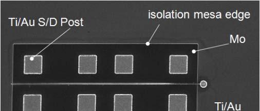
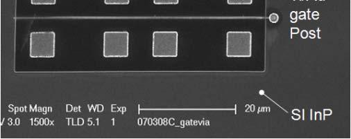
51 Target Device Parameters source contact metal gate sidewall gate dielectric drain contact N+ source N+ drain quantum well / channel barrier substrate well : 12 2 n ~ 5 10 / cm, 5 nm thick n s / cm, 5 nm thick ns = / cm 2 2 ( Ω μm ) /( 25 nm wide contact) = 10 Ω μm
52 Device Structure & Process Flow


53 Device Fabrication: Goals & Challenges III-V HEMTs are built like this Source Gate Drain K Shinohara and most...and most III-V MOSFETs are built like this

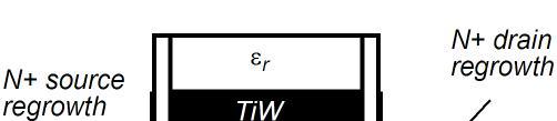
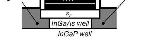
54 Device Fabrication: Goals & Challenges Yet, we are developing, at great effort, a structure like this N+ source regrowth ε r TiW ε r InGaAs well InP well barrier N+ drain regrowth Why? Source Gate Drain K Shinohara

55 Why not just build HEMTs? Gate Barrier is Low! Gate barrier is low: ~0.6 ev Source Gate Drain K Shinohara Tunneling through barrier sets minimum thickness Emission over barrier limits 2D carrier density E c E F E c E F E well-γ E well-γ At N s = / cm 2, ( E f E ) ~ 0.6 ev c
56 Why not just build HEMTs? Gate barrier also lies under source / drain contacts Source Gate Drain N+ layer widegap barrier layer K Shinohara low leakage: need high barrier under gate low resistance: need low barrier under contacts E c E c E F E F E well-γ N+ cap layer E well-γ
57 The Structure We Need -- is Much Like a Si MOSFET source contact metal gate sidewall gate dielectric drain contact N+ source N+ drain quantum well / channel barrier no gate barrier under S/D contacts substrate high-k gate barrier Overlap between gate and N+ source/drain How do we make this device?
58 S/D Regrowth Process Flow


.")
59 Regrown S/D FETs: Versions Wistey et al 2008 MBE conference regrowth under sidewalls planar regrowth need thin sidewalls (now ~20-30 nm)..or doping under sidewalls


60 S/D Regrowth by Migration-Enhanced Epitaxy Wistey et al 2008 MBE conference MBE growth is line-of-sight gaps in regrowth near gate edges MEE provides surface migration during regrowth eliminates gaps SEM Cross Section SEM Side View (Oblique) Top of gate SiO2 dummy gate SiO2 dummy gate Side of gate InGaAs Regrowth Original Interface InGaAs Regrowth No gaps Smooth surfaces. SEM: Greg Burek SEM: Uttam Singisetti High Si activation (4x10 19 cm -3 ). Quasi-selective: no growth on sidewalls 6 0

61 Self-Aligned Planar III-V MOSFETs by Regrowth Mo contact metal N+ InGaAs regrowth, Mo contact metal Wistey Singisetti Burek Lee gate
62 Self-Aligned Planar III-V MOSFETs by Regrowth Wistey Singisetti Burek Lee
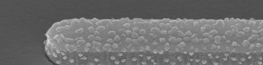
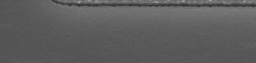
63 Regrown S/D FETs: Images
64 Regrown S/D FETs: Images
65 III-V MOS
66 InGaAs / InP MOSFETs: Why and Why Not low m*/m 0 high v carrier more current low m*/m 0 low density of states less current ballistic / degenerate calculation Error bars on Si data points correct for (E f - E c )>> kt approximation n = # band minima c dos,o = density of states capacitance for m*=m o & n=1 K nm, n=6 0.4 nm, n=6 0.8 nm, n=1 1.0 nm, n=1 3/ 2 ma Vgs Vth J = K 84, μm 1V * n ( m m ) 1/ 2 o where K = * c dos, o m 1 + n cox mo 3/ 2 0 EOT includes wavefunction depth (0.5 nm for 3.5 nm InGaAs well) m*/m o Low m* impairs vertical (hence L g ) scaling ; InGaAs no good below 22-nm. InGaAs allows very low access resistance Si wins if high-k scales below 0.6 nm EOT; otherwise, III-V has a chance
67 InGaAs/InP Channel MOSFETs for VLSI Low-m* materials are beneficial only if EOT cannot scale below ~1/2 nm Devices cannot scale much below 22 nm Lg limits IC density Little CV/I benefit in gate lengths below 22 nm Lg Need device structure with very low access resistance radical re-work of device structure & process flow Gate dielectrics, III-V growth on Si: also under intensive development
Technology Development & Design for 22 nm InGaAs/InP-channel MOSFETs
 2008 Indium Phosphide and Related Materials Conference, May, Versailles, France Technology Development & Design for 22 nm InGaAs/InP-channel MOSFETs M. Rodwell University of California, Santa Barbara M.
CMPEN 411 VLSI Digital Circuits. Lecture 03: MOS Transistor
 CMPEN 411 VLSI Digital Circuits Lecture 03: MOS Transistor Kyusun Choi [Adapted from Rabaey s Digital Integrated Circuits, Second Edition, 2003 J. Rabaey, A. Chandrakasan, B. Nikolic] CMPEN 411 L03 S.1
Lecture 3: Transistor as an thermonic switch
 Lecture 3: Transistor as an thermonic switch 2016-01-21 Lecture 3, High Speed Devices 2016 1 Lecture 3: Transistors as an thermionic switch Reading Guide: 54-57 in Jena Transistor metrics Reservoir equilibrium
III-V CMOS: What have we learned from HEMTs? J. A. del Alamo, D.-H. Kim 1, T.-W. Kim, D. Jin, and D. A. Antoniadis
 III-V CMOS: What have we learned from HEMTs? J. A. del Alamo, D.-H. Kim 1, T.-W. Kim, D. Jin, and D. A. Antoniadis Microsystems Technology Laboratories, MIT 1 presently with Teledyne Scientific 23rd International
Prospects for Ge MOSFETs
 Prospects for Ge MOSFETs Sematech Workshop December 4, 2005 Dimitri A. Antoniadis Microsystems Technology Laboratories MIT Sematech Workshop 2005 1 Channel Transport - I D I D =WQ i (x 0 )v xo v xo : carrier
ECE 497 JS Lecture - 12 Device Technologies
 ECE 497 JS Lecture - 12 Device Technologies Spring 2004 Jose E. Schutt-Aine Electrical & Computer Engineering University of Illinois jose@emlab.uiuc.edu 1 NMOS Transistor 2 ρ Source channel charge density
ESE 570: Digital Integrated Circuits and VLSI Fundamentals
 ESE 570: Digital Integrated Circuits and VLSI Fundamentals Lec 4: January 23, 2018 MOS Transistor Theory, MOS Model Penn ESE 570 Spring 2018 Khanna Lecture Outline! CMOS Process Enhancements! Semiconductor
Final Examination EE 130 December 16, 1997 Time allotted: 180 minutes
 Final Examination EE 130 December 16, 1997 Time allotted: 180 minutes Problem 1: Semiconductor Fundamentals [30 points] A uniformly doped silicon sample of length 100µm and cross-sectional area 100µm 2
Lecture 6: 2D FET Electrostatics
 Lecture 6: 2D FET Electrostatics 2016-02-01 Lecture 6, High Speed Devices 2014 1 Lecture 6: III-V FET DC I - MESFETs Reading Guide: Liu: 323-337 (he mainly focuses on the single heterostructure FET) Jena:
Quantum-size effects in sub-10 nm fin width InGaAs finfets
 Quantum-size effects in sub-10 nm fin width InGaAs finfets Alon Vardi, Xin Zhao, and Jesús A. del Alamo Microsystems Technology Laboratories, MIT December 9, 2015 Sponsors: DTRA NSF (E3S STC) Northrop
Device Models (PN Diode, MOSFET )
") Device Models (PN Diode, MOSFET ) Instructor: Steven P. Levitan steve@ece.pitt.edu TA: Gayatri Mehta, José Martínez Book: Digital Integrated Circuits: A Design Perspective; Jan Rabaey Lab Notes: Handed
Device Models (PN Diode, MOSFET ) Instructor: Steven P. Levitan steve@ece.pitt.edu TA: Gayatri Mehta, José Martínez Book: Digital Integrated Circuits: A Design Perspective; Jan Rabaey Lab Notes: Handed
Metal-oxide-semiconductor field effect transistors (2 lectures)
") Metal-ide-semiconductor field effect transistors ( lectures) MOS physics (brief in book) Current-voltage characteristics - pinch-off / channel length modulation - weak inversion - velocity saturation -
Metal-ide-semiconductor field effect transistors ( lectures) MOS physics (brief in book) Current-voltage characteristics - pinch-off / channel length modulation - weak inversion - velocity saturation -
Scaling Issues in Planar FET: Dual Gate FET and FinFETs
 Scaling Issues in Planar FET: Dual Gate FET and FinFETs Lecture 12 Dr. Amr Bayoumi Fall 2014 Advanced Devices (EC760) Arab Academy for Science and Technology - Cairo 1 Outline Scaling Issues for Planar
MOSFET: Introduction
 E&CE 437 Integrated VLSI Systems MOS Transistor 1 of 30 MOSFET: Introduction Metal oxide semiconductor field effect transistor (MOSFET) or MOS is widely used for implementing digital designs Its major
Simple Theory of the Ballistic Nanotransistor
 Simple Theory of the Ballistic Nanotransistor Mark Lundstrom Purdue University Network for Computational Nanoechnology outline I) Traditional MOS theory II) A bottom-up approach III) The ballistic nanotransistor
EEC 118 Lecture #2: MOSFET Structure and Basic Operation. Rajeevan Amirtharajah University of California, Davis Jeff Parkhurst Intel Corporation
 EEC 118 Lecture #2: MOSFET Structure and Basic Operation Rajeevan Amirtharajah University of California, Davis Jeff Parkhurst Intel Corporation Announcements Lab 1 this week, report due next week Bring
Comparison of Ultra-Thin InAs and InGaAs Quantum Wells and Ultra-Thin-Body Surface-Channel MOSFETs
 Comparison of Ultra-Thin InAs and InGaAs Quantum Wells and Ultra-Thin-Body Surface-Channel MOSFETs Cheng-Ying Huang 1, Sanghoon Lee 1, Evan Wilson 3, Pengyu Long 3, Michael Povolotskyi 3, Varistha Chobpattana
Lecture 29 - The Long Metal-Oxide-Semiconductor Field-Effect Transistor (cont.) April 20, 2007
 April 20, 2007") 6.720J/3.43J - Integrated Microelectronic Devices - Spring 2007 Lecture 29-1 Lecture 29 - The Long Metal-Oxide-Semiconductor Field-Effect Transistor (cont.) April 20, 2007 Contents: 1. Non-ideal and second-order
6.720J/3.43J - Integrated Microelectronic Devices - Spring 2007 Lecture 29-1 Lecture 29 - The Long Metal-Oxide-Semiconductor Field-Effect Transistor (cont.) April 20, 2007 Contents: 1. Non-ideal and second-order
MOS Transistors. Prof. Krishna Saraswat. Department of Electrical Engineering Stanford University Stanford, CA
 MOS Transistors Prof. Krishna Saraswat Department of Electrical Engineering S Stanford, CA 94305 saraswat@stanford.edu 1 1930: Patent on the Field-Effect Transistor! Julius Lilienfeld filed a patent describing
EECS130 Integrated Circuit Devices
 EECS130 Integrated Circuit Devices Professor Ali Javey 10/30/2007 MOSFETs Lecture 4 Reading: Chapter 17, 19 Announcements The next HW set is due on Thursday. Midterm 2 is next week!!!! Threshold and Subthreshold
The Prospects for III-Vs
 10 nm CMOS: The Prospects for III-Vs J. A. del Alamo, Dae-Hyun Kim 1, Donghyun Jin, and Taewoo Kim Microsystems Technology Laboratories, MIT 1 Presently with Teledyne Scientific 2010 European Materials
The Devices. Digital Integrated Circuits A Design Perspective. Jan M. Rabaey Anantha Chandrakasan Borivoje Nikolic. July 30, 2002
 Digital Integrated Circuits A Design Perspective Jan M. Rabaey Anantha Chandrakasan Borivoje Nikolic The Devices July 30, 2002 Goal of this chapter Present intuitive understanding of device operation Introduction
MOS Transistor I-V Characteristics and Parasitics
 ECEN454 Digital Integrated Circuit Design MOS Transistor I-V Characteristics and Parasitics ECEN 454 Facts about Transistors So far, we have treated transistors as ideal switches An ON transistor passes
Device Models (PN Diode, MOSFET )
") Device Models (PN Diode, MOSFET ) Instructor: Steven P. Levitan steve@ece.pitt.edu TA: Gayatri Mehta, José Martínez Book: Digital Integrated Circuits: A Design Perspective; Jan Rabaey Lab Notes: Handed
Device Models (PN Diode, MOSFET ) Instructor: Steven P. Levitan steve@ece.pitt.edu TA: Gayatri Mehta, José Martínez Book: Digital Integrated Circuits: A Design Perspective; Jan Rabaey Lab Notes: Handed
Spring Semester 2012 Final Exam
 Spring Semester 2012 Final Exam Note: Show your work, underline results, and always show units. Official exam time: 2.0 hours; an extension of at least 1.0 hour will be granted to anyone. Materials parameters
Performance Analysis of 60-nm Gate-Length III-V InGaAs HEMTs: Simulations Versus Experiments
 Purdue University Purdue e-pubs Birck and NCN Publications Birck Nanotechnology Center 7-2009 Performance Analysis of 60-nm Gate-Length III-V InGaAs HEMTs: Simulations Versus Experiments Neophytou Neophytos
! CMOS Process Enhancements. ! Semiconductor Physics. " Band gaps. " Field Effects. ! MOS Physics. " Cut-off. " Depletion.
 ESE 570: Digital Integrated Circuits and VLSI Fundamentals Lec 4: January 3, 018 MOS Transistor Theory, MOS Model Lecture Outline! CMOS Process Enhancements! Semiconductor Physics " Band gaps " Field Effects!
Lecture 4: CMOS Transistor Theory
 Introduction to CMOS VLSI Design Lecture 4: CMOS Transistor Theory David Harris, Harvey Mudd College Kartik Mohanram and Steven Levitan University of Pittsburgh Outline q Introduction q MOS Capacitor q
ESE 570: Digital Integrated Circuits and VLSI Fundamentals
 ESE 570: Digital Integrated Circuits and VLSI Fundamentals Lec 4: January 29, 2019 MOS Transistor Theory, MOS Model Penn ESE 570 Spring 2019 Khanna Lecture Outline! CMOS Process Enhancements! Semiconductor
MOS Transistor Theory
 CHAPTER 3 MOS Transistor Theory Outline 2 1. Introduction 2. Ideal I-V Characteristics 3. Nonideal I-V Effects 4. C-V Characteristics 5. DC Transfer Characteristics 6. Switch-level RC Delay Models MOS
Lecture 8: Ballistic FET I-V
 Lecture 8: Ballistic FET I-V 1 Lecture 1: Ballistic FETs Jena: 61-70 Diffusive Field Effect Transistor Source Gate L g >> l Drain Source V GS Gate Drain I D Mean free path much shorter than channel length
Long Channel MOS Transistors
 Long Channel MOS Transistors The theory developed for MOS capacitor (HO #2) can be directly extended to Metal-Oxide-Semiconductor Field-Effect transistors (MOSFET) by considering the following structure:
Microsystems Technology Laboratories, MIT. Teledyne Scientific Company (TSC)
") Extraction of Virtual-Source Injection Velocity in sub-100 nm III-V HFETs 1,2) D.-H. Kim, 1) J. A. del Alamo, 1) D. A. Antoniadis and 2) B. Brar 1) Microsystems Technology Laboratories, MIT 2) Teledyne
Extraction of Virtual-Source Injection Velocity in sub-100 nm III-V HFETs 1,2) D.-H. Kim, 1) J. A. del Alamo, 1) D. A. Antoniadis and 2) B. Brar 1) Microsystems Technology Laboratories, MIT 2) Teledyne
Chapter 5 MOSFET Theory for Submicron Technology
 Chapter 5 MOSFET Theory for Submicron Technology Short channel effects Other small geometry effects Parasitic components Velocity saturation/overshoot Hot carrier effects ** Majority of these notes are
The Devices. Digital Integrated Circuits A Design Perspective. Jan M. Rabaey Anantha Chandrakasan Borivoje Nikolic. July 30, 2002
 igital Integrated Circuits A esign Perspective Jan M. Rabaey Anantha Chandrakasan Borivoje Nikolic The evices July 30, 2002 Goal of this chapter Present intuitive understanding of device operation Introduction
Digital Integrated Circuits A Design Perspective. Jan M. Rabaey Anantha Chandrakasan Borivoje Nikolic. The Devices. July 30, Devices.
 Digital Integrated Circuits A Design Perspective Jan M. Rabaey Anantha Chandrakasan Borivoje Nikolic The July 30, 2002 1 Goal of this chapter Present intuitive understanding of device operation Introduction
The Devices. Jan M. Rabaey
 The Devices Jan M. Rabaey Goal of this chapter Present intuitive understanding of device operation Introduction of basic device equations Introduction of models for manual analysis Introduction of models
MSE 310/ECE 340: Electrical Properties of Materials Fall 2014 Department of Materials Science and Engineering Boise State University
 MSE 310/ECE 340: Electrical Properties of Materials Fall 2014 Department of Materials Science and Engineering Boise State University Practice Final Exam 1 Read the questions carefully Label all figures
Lecture 5: CMOS Transistor Theory
 Lecture 5: CMOS Transistor Theory Slides courtesy of Deming Chen Slides based on the initial set from David Harris CMOS VLSI Design Outline q q q q q q q Introduction MOS Capacitor nmos I-V Characteristics
High Mobility Materials and Novel Device Structures for High Performance Nanoscale MOSFETs
 High Mobility Materials and Novel Device Structures for High Performance Nanoscale MOSFETs Prof. (Dr.) Tejas Krishnamohan Department of Electrical Engineering Stanford University, CA & Intel Corporation
Lecture 12: MOS Capacitors, transistors. Context
 Lecture 12: MOS Capacitors, transistors Context In the last lecture, we discussed PN diodes, and the depletion layer into semiconductor surfaces. Small signal models In this lecture, we will apply those
Components Research, TMG Intel Corporation *QinetiQ. Contact:
 1 High-Performance 4nm Gate Length InSb P-Channel Compressively Strained Quantum Well Field Effect Transistors for Low-Power (V CC =.5V) Logic Applications M. Radosavljevic,, T. Ashley*, A. Andreev*, S.
The Devices. Devices
 The The MOS Transistor Gate Oxyde Gate Source n+ Polysilicon Drain n+ Field-Oxyde (SiO 2 ) p-substrate p+ stopper Bulk Contact CROSS-SECTION of NMOS Transistor Cross-Section of CMOS Technology MOS transistors
Application II: The Ballistic Field-E ect Transistor
 Chapter 1 Application II: The Ballistic Field-E ect Transistor 1.1 Introduction In this chapter, we apply the formalism we have developed for charge currents to understand the output characteristics of
and V DS V GS V T (the saturation region) I DS = k 2 (V GS V T )2 (1+ V DS )
 I DS = k 2 (V GS V T )2 (1+ V DS )") ECE 4420 Spring 2005 Page 1 FINAL EXAMINATION NAME SCORE /100 Problem 1O 2 3 4 5 6 7 Sum Points INSTRUCTIONS: This exam is closed book. You are permitted four sheets of notes (three of which are your sheets
ECE 4420 Spring 2005 Page 1 FINAL EXAMINATION NAME SCORE /100 Problem 1O 2 3 4 5 6 7 Sum Points INSTRUCTIONS: This exam is closed book. You are permitted four sheets of notes (three of which are your sheets
Current mechanisms Exam January 27, 2012
 Current mechanisms Exam January 27, 2012 There are four mechanisms that typically cause currents to flow: thermionic emission, diffusion, drift, and tunneling. Explain briefly which kind of current mechanisms
Ultra-Scaled InAs HEMTs
 Performance Analysis of Ultra-Scaled InAs HEMTs Neerav Kharche 1, Gerhard Klimeck 1, Dae-Hyun Kim 2,3, Jesús. A. del Alamo 2, and Mathieu Luisier 1 1 Network for Computational ti Nanotechnology and Birck
SECTION: Circle one: Alam Lundstrom. ECE 305 Exam 5 SOLUTIONS: Spring 2016 April 18, 2016 M. A. Alam and M.S. Lundstrom Purdue University
 NAME: PUID: SECTION: Circle one: Alam Lundstrom ECE 305 Exam 5 SOLUTIONS: April 18, 2016 M A Alam and MS Lundstrom Purdue University This is a closed book exam You may use a calculator and the formula
Metallic: 2n 1. +n 2. =3q Armchair structure always metallic = 2
 Properties of CNT d = 2.46 n 2 2 1 + n1n2 + n2 2π Metallic: 2n 1 +n 2 =3q Armchair structure always metallic a) Graphite Valence(π) and Conduction(π*) states touch at six points(fermi points) Carbon Nanotube:
Section 12: Intro to Devices
 Section 12: Intro to Devices Extensive reading materials on reserve, including Robert F. Pierret, Semiconductor Device Fundamentals EE143 Ali Javey Bond Model of Electrons and Holes Si Si Si Si Si Si Si
Semiconductor Physics Problems 2015
 Semiconductor Physics Problems 2015 Page and figure numbers refer to Semiconductor Devices Physics and Technology, 3rd edition, by SM Sze and M-K Lee 1. The purest semiconductor crystals it is possible
Performance Analysis of Ultra-Scaled InAs HEMTs
 Purdue University Purdue e-pubs Birck and NCN Publications Birck Nanotechnology Center 2009 Performance Analysis of Ultra-Scaled InAs HEMTs Neerav Kharche Birck Nanotechnology Center and Purdue University,
Lecture 12: MOSFET Devices
 Lecture 12: MOSFET Devices Gu-Yeon Wei Division of Engineering and Applied Sciences Harvard University guyeon@eecs.harvard.edu Wei 1 Overview Reading S&S: Chapter 5.1~5.4 Supplemental Reading Background
! CMOS Process Enhancements. ! Semiconductor Physics. " Band gaps. " Field Effects. ! MOS Physics. " Cut-off. " Depletion.
 ESE 570: Digital Integrated Circuits and VLSI Fundamentals Lec 4: January 9, 019 MOS Transistor Theory, MOS Model Lecture Outline CMOS Process Enhancements Semiconductor Physics Band gaps Field Effects
6.012 Electronic Devices and Circuits
 Page 1 of 10 YOUR NAME Department of Electrical Engineering and Computer Science Massachusetts Institute of Technology 6.012 Electronic Devices and Circuits Exam No. 2 Thursday, November 5, 2009 7:30 to
ECE 342 Electronic Circuits. 3. MOS Transistors
 ECE 342 Electronic Circuits 3. MOS Transistors Jose E. Schutt-Aine Electrical & Computer Engineering University of Illinois jschutt@emlab.uiuc.edu 1 NMOS Transistor Typically L = 0.1 to 3 m, W = 0.2 to
EE105 Fall 2014 Microelectronic Devices and Circuits. NMOS Transistor Capacitances: Saturation Region
 EE105 Fall 014 Microelectronic Devices and Circuits Prof. Ming C. Wu wu@eecs.berkeley.edu 511 Sutardja Dai Hall (SDH) 1 NMOS Transistor Capacitances: Saturation Region Drain no longer connected to channel
Erik Lind
 High-Speed Devices, 2011 Erik Lind (Erik.Lind@ftf.lth.se) Course consists of: 30 h Lectures (H322, and Fys B check schedule) 8h Excercises 2x2h+4h Lab Excercises (2 Computer simulations, 4 RF measurment
The Critical Role of Quantum Capacitance in Compact Modeling of Nano-Scaled and Nanoelectronic Devices
 The Critical Role of Quantum Capacitance in Compact Modeling of Nano-Scaled and Nanoelectronic Devices Zhiping Yu and Jinyu Zhang Institute of Microelectronics Tsinghua University, Beijing, China yuzhip@tsinghua.edu.cn
Stretching the Barriers An analysis of MOSFET Scaling. Presenters (in order) Zeinab Mousavi Stephanie Teich-McGoldrick Aseem Jain Jaspreet Wadhwa
 Zeinab Mousavi Stephanie Teich-McGoldrick Aseem Jain Jaspreet Wadhwa") Stretching the Barriers An analysis of MOSFET Scaling Presenters (in order) Zeinab Mousavi Stephanie Teich-McGoldrick Aseem Jain Jaspreet Wadhwa Why Small? Higher Current Lower Gate Capacitance Higher
Stretching the Barriers An analysis of MOSFET Scaling Presenters (in order) Zeinab Mousavi Stephanie Teich-McGoldrick Aseem Jain Jaspreet Wadhwa Why Small? Higher Current Lower Gate Capacitance Higher
Chapter 4 Field-Effect Transistors
 Chapter 4 Field-Effect Transistors Microelectronic Circuit Design Richard C. Jaeger Travis N. Blalock 5/5/11 Chap 4-1 Chapter Goals Describe operation of MOSFETs. Define FET characteristics in operation
Carbon Nanotube Electronics
 Carbon Nanotube Electronics Jeorg Appenzeller, Phaedon Avouris, Vincent Derycke, Stefan Heinz, Richard Martel, Marko Radosavljevic, Jerry Tersoff, Shalom Wind H.-S. Philip Wong hspwong@us.ibm.com IBM T.J.
EE105 - Fall 2005 Microelectronic Devices and Circuits
 EE105 - Fall 005 Microelectronic Devices and Circuits ecture 7 MOS Transistor Announcements Homework 3, due today Homework 4 due next week ab this week Reading: Chapter 4 1 ecture Material ast lecture
ESE 570: Digital Integrated Circuits and VLSI Fundamentals
 ESE 570: Digital Integrated Circuits and VLSI Fundamentals Lec 4: January 24, 2017 MOS Transistor Theory, MOS Model Penn ESE 570 Spring 2017 Khanna Lecture Outline! Semiconductor Physics " Band gaps "
EE105 - Fall 2006 Microelectronic Devices and Circuits
 EE105 - Fall 2006 Microelectronic Devices and Circuits Prof. Jan M. Rabaey (jan@eecs) Lecture 7: MOS Transistor Some Administrative Issues Lab 2 this week Hw 2 due on We Hw 3 will be posted same day MIDTERM
EE5311- Digital IC Design
 EE5311- Digital IC Design Module 1 - The Transistor Janakiraman V Assistant Professor Department of Electrical Engineering Indian Institute of Technology Madras Chennai October 28, 2017 Janakiraman, IITM
The Devices: MOS Transistors
 The Devices: MOS Transistors References: Semiconductor Device Fundamentals, R. F. Pierret, Addison-Wesley Digital Integrated Circuits: A Design Perspective, J. Rabaey et.al. Prentice Hall NMOS Transistor
VLSI Design and Simulation
 VLSI Design and Simulation Performance Characterization Topics Performance Characterization Resistance Estimation Capacitance Estimation Inductance Estimation Performance Characterization Inverter Voltage
ECE-305: Fall 2017 MOS Capacitors and Transistors
 ECE-305: Fall 2017 MOS Capacitors and Transistors Pierret, Semiconductor Device Fundamentals (SDF) Chapters 15+16 (pp. 525-530, 563-599) Professor Peter Bermel Electrical and Computer Engineering Purdue
VLSI Design The MOS Transistor
 VLSI Design The MOS Transistor Frank Sill Torres Universidade Federal de Minas Gerais (UFMG), Brazil VLSI Design: CMOS Technology 1 Outline Introduction MOS Capacitor nmos I-V Characteristics pmos I-V
The Future of CMOS. David Pulfrey. CHRONOLOGY of the FET. Lecture Lilienfeld s patent (BG FET) 1965 Commercialization (Fairchild)
 1965 Commercialization (Fairchild)") The Future of CMOS David Pulfrey 1 CHRONOLOGY of the FET 1933 Lilienfeld s patent (BG FET) 1965 Commercialization (Fairchild) 1991 The most abundant object made by mankind (C.T. Sah) 2003 The 10 nm FET
The Future of CMOS David Pulfrey 1 CHRONOLOGY of the FET 1933 Lilienfeld s patent (BG FET) 1965 Commercialization (Fairchild) 1991 The most abundant object made by mankind (C.T. Sah) 2003 The 10 nm FET
II III IV V VI B C N. Al Si P S. Zn Ga Ge As Se Cd In Sn Sb Te. Silicon (Si) the dominating material in IC manufacturing
 the dominating material in IC manufacturing") II III IV V VI B N Al Si P S Zn Ga Ge As Se d In Sn Sb Te Silicon (Si) the dominating material in I manufacturing ompound semiconductors III - V group: GaAs GaN GaSb GaP InAs InP InSb... The Energy Band
II III IV V VI B N Al Si P S Zn Ga Ge As Se d In Sn Sb Te Silicon (Si) the dominating material in I manufacturing ompound semiconductors III - V group: GaAs GaN GaSb GaP InAs InP InSb... The Energy Band
Appendix 1: List of symbols
 Appendix 1: List of symbols Symbol Description MKS Units a Acceleration m/s 2 a 0 Bohr radius m A Area m 2 A* Richardson constant m/s A C Collector area m 2 A E Emitter area m 2 b Bimolecular recombination
ECE 546 Lecture 10 MOS Transistors
 ECE 546 Lecture 10 MOS Transistors Spring 2018 Jose E. Schutt-Aine Electrical & Computer Engineering University of Illinois jesa@illinois.edu NMOS Transistor NMOS Transistor N-Channel MOSFET Built on p-type
FIELD-EFFECT TRANSISTORS
 FIEL-EFFECT TRANSISTORS 1 Semiconductor review 2 The MOS capacitor 2 The enhancement-type N-MOS transistor 3 I-V characteristics of enhancement MOSFETS 4 The output characteristic of the MOSFET in saturation
Practice 3: Semiconductors
 Practice 3: Semiconductors Digital Electronic Circuits Semester A 2012 VLSI Fabrication Process VLSI Very Large Scale Integration The ability to fabricate many devices on a single substrate within a given
THz Bipolar Transistor Circuits: Technical Feasibility, Technology Development, Integrated Circuit Results
 Plenary, 2008 IEEE-SI Symposium, October 12, 2008 THz Bipolar Transistor ircuits: Technical Feasibility, Technology Development, Integrated ircuit Results Mark Rodwell University of alifornia, Santa Barbara
MOS Transistor Properties Review
 MOS Transistor Properties Review 1 VLSI Chip Manufacturing Process Photolithography: transfer of mask patterns to the chip Diffusion or ion implantation: selective doping of Si substrate Oxidation: SiO
EE410 vs. Advanced CMOS Structures
 EE410 vs. Advanced CMOS Structures Prof. Krishna S Department of Electrical Engineering S 1 EE410 CMOS Structure P + poly-si N + poly-si Al/Si alloy LPCVD PSG P + P + N + N + PMOS N-substrate NMOS P-well
Journal of Electron Devices, Vol. 18, 2013, pp JED [ISSN: ]
![Journal of Electron Devices, Vol. 18, 2013, pp JED [ISSN: ]](/thumbs/86/93990983.jpg "Journal of Electron Devices, Vol. 18, 2013, pp JED [ISSN: ]") DrainCurrent-Id in linearscale(a/um) Id in logscale Journal of Electron Devices, Vol. 18, 2013, pp. 1582-1586 JED [ISSN: 1682-3427 ] SUITABILITY OF HIGH-k GATE DIELECTRICS ON THE DEVICE PERFORMANCE AND
DrainCurrent-Id in linearscale(a/um) Id in logscale Journal of Electron Devices, Vol. 18, 2013, pp. 1582-1586 JED [ISSN: 1682-3427 ] SUITABILITY OF HIGH-k GATE DIELECTRICS ON THE DEVICE PERFORMANCE AND
A Compact Analytical Modelling of the Electrical Characteristics of Submicron Channel MOSFETs
 ROMANIAN JOURNAL OF INFORMATION SCIENCE AND TECHNOLOGY Volume 11, Number 4, 2008, 383 395 A Compact Analytical Modelling of the Electrical Characteristics of Submicron Channel MOSFETs Andrei SEVCENCO,
MOS CAPACITOR AND MOSFET
 EE336 Semiconductor Devices 1 MOS CAPACITOR AND MOSFET Dr. Mohammed M. Farag Ideal MOS Capacitor Semiconductor Devices Physics and Technology Chapter 5 EE336 Semiconductor Devices 2 MOS Capacitor Structure
P. R. Nelson 1 ECE418 - VLSI. Midterm Exam. Solutions
 P. R. Nelson 1 ECE418 - VLSI Midterm Exam Solutions 1. (8 points) Draw the cross-section view for A-A. The cross-section view is as shown below.. ( points) Can you tell which of the metal1 regions is the
Microelectronics Part 1: Main CMOS circuits design rules
 GBM8320 Dispositifs Médicaux telligents Microelectronics Part 1: Main CMOS circuits design rules Mohamad Sawan et al. Laboratoire de neurotechnologies Polystim! http://www.cours.polymtl.ca/gbm8320/! med-amine.miled@polymtl.ca!
CHAPTER 5 EFFECT OF GATE ELECTRODE WORK FUNCTION VARIATION ON DC AND AC PARAMETERS IN CONVENTIONAL AND JUNCTIONLESS FINFETS
 98 CHAPTER 5 EFFECT OF GATE ELECTRODE WORK FUNCTION VARIATION ON DC AND AC PARAMETERS IN CONVENTIONAL AND JUNCTIONLESS FINFETS In this chapter, the effect of gate electrode work function variation on DC
Extensive reading materials on reserve, including
 Section 12: Intro to Devices Extensive reading materials on reserve, including Robert F. Pierret, Semiconductor Device Fundamentals EE143 Ali Javey Bond Model of Electrons and Holes Si Si Si Si Si Si Si
Lecture #27. The Short Channel Effect (SCE)
") Lecture #27 ANNOUNCEMENTS Design Project: Your BJT design should meet the performance specifications to within 10% at both 300K and 360K. ( β dc > 45, f T > 18 GHz, V A > 9 V and V punchthrough > 9 V )
Lecture #27 ANNOUNCEMENTS Design Project: Your BJT design should meet the performance specifications to within 10% at both 300K and 360K. ( β dc > 45, f T > 18 GHz, V A > 9 V and V punchthrough > 9 V )
Electric Field-Dependent Charge-Carrier Velocity in Semiconducting Carbon. Nanotubes. Yung-Fu Chen and M. S. Fuhrer
 Electric Field-Dependent Charge-Carrier Velocity in Semiconducting Carbon Nanotubes Yung-Fu Chen and M. S. Fuhrer Department of Physics and Center for Superconductivity Research, University of Maryland,
ECE 342 Electronic Circuits. Lecture 6 MOS Transistors
 ECE 342 Electronic Circuits Lecture 6 MOS Transistors Jose E. Schutt-Aine Electrical & Computer Engineering University of Illinois jesa@illinois.edu 1 NMOS Transistor Typically L = 0.1 to 3 m, W = 0.2
Scaling of MOS Circuits. 4. International Technology Roadmap for Semiconductors (ITRS) 6. Scaling factors for device parameters
 6. Scaling factors for device parameters") 1 Scaling of MOS Circuits CONTENTS 1. What is scaling?. Why scaling? 3. Figure(s) of Merit (FoM) for scaling 4. International Technology Roadmap for Semiconductors (ITRS) 5. Scaling models 6. Scaling factors
1 Scaling of MOS Circuits CONTENTS 1. What is scaling?. Why scaling? 3. Figure(s) of Merit (FoM) for scaling 4. International Technology Roadmap for Semiconductors (ITRS) 5. Scaling models 6. Scaling factors
nmosfet Schematic Four structural masks: Field, Gate, Contact, Metal. Reverse doping polarities for pmosfet in N-well.
 nmosfet Schematic Four structural masks: Field, Gate, Contact, Metal. Reverse doping polarities for pmosfet in N-well. nmosfet Schematic 0 y L n + source n + drain depletion region polysilicon gate x z
Long-channel MOSFET IV Corrections
 Long-channel MOSFET IV orrections Three MITs of the Day The body ect and its influence on long-channel V th. Long-channel subthreshold conduction and control (subthreshold slope S) Scattering components
ECE 305: Fall MOSFET Energy Bands
 ECE 305: Fall 2016 MOSFET Energy Bands Professor Peter Bermel Electrical and Computer Engineering Purdue University, West Lafayette, IN USA pbermel@purdue.edu Pierret, Semiconductor Device Fundamentals
Field effect = Induction of an electronic charge due to an electric field Example: Planar capacitor
 JFETs AND MESFETs Introduction Field effect = Induction of an electronic charge due to an electric field Example: Planar capacitor Why would an FET made of a planar capacitor with two metal plates, as
ESE370: Circuit-Level Modeling, Design, and Optimization for Digital Systems
 ESE370: Circuit-Level Modeling, Design, and Optimization for Digital Systems Lec 6: September 14, 2015 MOS Model You are Here: Transistor Edition! Previously: simple models (0 and 1 st order) " Comfortable
Lecture 11: MOS Transistor
 Lecture 11: MOS Transistor Prof. Niknejad Lecture Outline Review: MOS Capacitors Regions MOS Capacitors (3.8 3.9) CV Curve Threshold Voltage MOS Transistors (4.1 4.3): Overview Cross-section and layout
S=0.7 [0.5x per 2 nodes] ESE370: Circuit-Level Modeling, Design, and Optimization for Digital Systems. Today. Scaling ITRS Roadmap
![S=0.7 [0.5x per 2 nodes] ESE370: Circuit-Level Modeling, Design, and Optimization for Digital Systems. Today. Scaling ITRS Roadmap](/thumbs/92/110446830.jpg "S=0.7 [0.5x per 2 nodes] ESE370: Circuit-Level Modeling, Design, and Optimization for Digital Systems. Today. Scaling ITRS Roadmap") ESE370: Circuit-Level Modeling, Design, and Optimization for Digital Systems Day 15: October 4, 2013 Scaling Today VLSI Scaling Trends/Disciplines Effects Alternatives (cheating) 1 2 Scaling ITRS Roadmap
ESE370: Circuit-Level Modeling, Design, and Optimization for Digital Systems Day 15: October 4, 2013 Scaling Today VLSI Scaling Trends/Disciplines Effects Alternatives (cheating) 1 2 Scaling ITRS Roadmap
ECE-343 Test 1: Feb 10, :00-8:00pm, Closed Book. Name : SOLUTION
 ECE-343 Test : Feb 0, 00 6:00-8:00pm, Closed Book Name : SOLUTION C Depl = C J0 + V R /V o ) m C Diff = τ F g m ω T = g m C µ + C π ω T = g m I / D C GD + C or V OV GS b = τ i τ i = R i C i ω H b Z = Z
LECTURE 3 MOSFETS II. MOS SCALING What is Scaling?
 LECTURE 3 MOSFETS II Lecture 3 Goals* * Understand constant field and constant voltage scaling and their effects. Understand small geometry effects for MOS transistors and their implications modeling and
Lecture 3: CMOS Transistor Theory
 Lecture 3: CMOS Transistor Theory Outline Introduction MOS Capacitor nmos I-V Characteristics pmos I-V Characteristics Gate and Diffusion Capacitance 2 Introduction So far, we have treated transistors