Complete Surface-Potential Modeling Approach Implemented in the HiSIM Compact Model Family for Any MOSFET Type
|
|
|
- Laurel Dickerson
- 5 years ago
- Views:
Transcription
1 Complete Surface-Potential Modeling Approach Implemented in the HiSIM Compact Model Family for Any MOSFET Type WCM in Boston 15. June, 2011 M. Miura-Mattausch, M. Miyake, H. Kikuchihara, U. Feldmann and H. J. Mattausch HiSIM Team, Hiroshima University HiSIM 1
2 Basic Device Equations s Gradual-Channel Approximation Charge-Sheet Approximation reduced to surface potential φ s HiSIM 2
3 Property of Surface-Potential Model Q(φ) = ν = μ E: velocity : mobility The surface potential consistently determines charges, capacitances and currents under all operating conditions. HiSIM 3
4 Relationship among Device Properties (at drain side) (at source side) HiSIM 4
5 Specific Feature of Surface-potential Model one equation for all bias conditions HiSIM 5

6 Model Extraction for 45nm Technology W g /L g =2μm/200nm W g /L g =2μm/40nm Measurement HiSIM2 one model for any device sizes without binning HiSIM 6
7 Current Derivatives for 45nm Technology Measurement HiSIM W g /L g = 2μm/40nm Beyond the 45nm generation nonphysical effects are getting obvious. HiSIM 7
8 Universal Mobility V ds =0.1V impurity concentration carrier concentration carrier mobility HiSIM 8
9 Requirements for RF Applications Harmonic Distortions Non-Quasi-Static Effect Noise Characteristics HiSIM 9
10 Feature of Potential-Based Model Current Equation: I = qnμe All physical quantities are function of surface potentials. Solution of Poisson s Equation Important RF characteristics are originated by the potential distribution along the channel. I-V characteristics reflect all important RF properties. Accurate parameter extraction for I-V characteristics is important. S. Matsumoto et al., IEIEC T E, E88-C, p. 247, S. Hosokawa et al., Ext. Abs. SSDM, pp. 20, M. Miura-Mattausch et al., IEEE TED, HiSIM 10
11 Descendant of MOSFET MG-MOSFET SOTB-MOSFET TFT SOI-MOSFET MOSFET HV-MOSFET MOS-Varactor IGBT HiSIM 11

12 HiSIM Family Bulk-MOSFET HiSIM2 High-Voltage MOSFET HiSIM_HV SOI MOSFET HiSIM-SOI Thin-Film Transistor Double-Gate MOSFET Insulated-Gate Bipolar Transistor HiSIM-TFT HiSIM-DG HiSIM-IGBT HiSIM 12

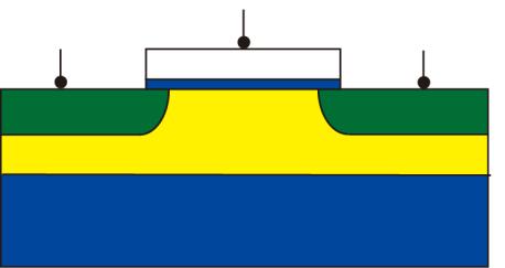
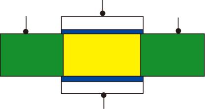
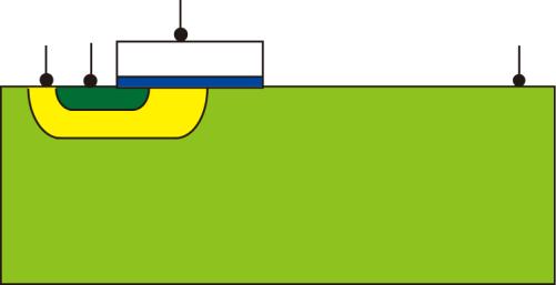
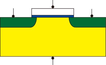
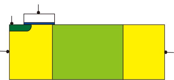
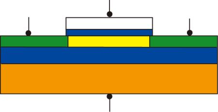
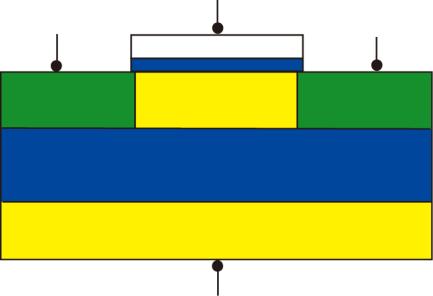
13 SOI-MOSFET Modeling many possible conditions Si Si substrate HiSIM 13

14 Poisson s Equation + Gauss s Law V φ φ gs fb s,soi b,soi s,soi Q+Q + Q + Q - V = φ - CFOX Qs,bulk = φs,bulk - CBOX 1 Q s,bulk + Qdep = φ 2 b,soi - C i dep b,soi s,bulk SOI Three surface potentials are solved simultaneously by iteration. Q b,soi φ b.soi φ s.soi Calculation results HiSIM 14
15 Smooth Transition among Conditions T SOI T BOX Conditi on Device PD Device DD Device DD Device FD HiSIM 15


16 C-V Characteristics T SOI =150nm T BOX =110nm : HiSIM-SOI : 2D-Device Sim. T SOI =50nm T BOX =110nm T SOI =50nm T BOX =50nm DEVICE1 DEVICE2 T SOI =25nm T BOX =110nm DEVICE3 DEVICE4 HiSIM 16
17 Potential Distribution in Thin-Body MOSFET device surface insulator Back surface potential is strongly dependent on T SOI. Consistent solution of Poisson s equation HiSIM 17
18 Device 4: Thin-Body SOI-MOSFET back-gate bias V bs dependence V bs φ b.soi φ s.soi HiSIM 18


19 Floating-Body Effect φ b.soi is unstable. symbol: 2D-Sim. line: HiSIM-SOI SOI bulk φ s.bulk φ b.soi φ s.soi BOX φ b.soi reduction change from FD to PD HiSIM 19


20 Charge Accumulation Impact Ionization: Include accumulation charge in the Poisson equation Increase the surface potential φ s0.soi Increase the inversion charge Q i according to V ds increase HiSIM 20
21 History Effect Transient Characteristics of the Floating-Body Effect Τ d : Time constant of Q h accumulation T d H. Toda et al., SSDM HiSIM 21

22 I d -V d Comparison with Measurements gds gds gds V sub = 0.0V V sub = 0.0V V sub = 0.0V V sub = 0.0V V sub = -1.5V V sub = -1.5V V sub = -1.5V V sub = -1.5V measurement HiSIM-SOI HiSIM 22
23 I d -V d Characteristics as a function of N SOI W g =0.25mm, L g =0.15mm N SOI (cm -3 ) = 1.0e16 2.0e16 5.0e16 Vds Vds Vds Vds Vds Vds Ids Ids Ids Ids Ids Ids Ids 1.0e17 2.0e17 5.0e17 Ids Ids 1.0e18 2.0e18 5.0e18 Vds Vds Vds enhanced floating body effect with increased N SOI HiSIM 23
24 Scalability Tests V th vs. N SOI for various V bs 0.6 V ds =0.05V, W g =10μm, L g =0.15 μm Threshold Voltage (V) Vsub = 0 to -3V step -1.0V e16 1.0e17 1.0e18 1.0e19 N SOI (cm -3 ) automatic FD PD shift HiSIM 24
25 HiSIM-SOI - Considering all possible induced charges in the Poisson equation - Solving the Poisson equation iteratively - Deriving accurate analytical solution as initial values Solving the Poisson equation in a consistent way is only a possibility to model all different structures and conditions within one model framework. HiSIM 25


26 carrier concentration T si =10nm gate gate HiSIM-DG V gs =1V V ds =0V T si T si =20nm gate gate T si =40nm gate gate T si Body potential is floating. The floating body potential makes modeling difficult. HiSIM 26
 φ s0 (V)")
27 Potential Dependence on T si and N sub N sub T Si φ s0 (V) φ s0 (V) HiSIM 27
28 C-V Characteristics Reduction of T si has only a small influence on the capacitance characteristics. HiSIM 28
29 Carrier Traps in TFT Source Gate Drain 1.E-05 Trap density small x y φ S0 Poly-Si φ SL Id(A) 1.E-07 1.E-09 large φ b0 Display Substrate (Insulator) φ bl 1.E-11 Traps 1.E Vg(V) HiSIM 29
30 Modeling of Trap Density Grain Boundaries Poly-Si film Traps uniformly distributed in crystal Si Simplified Model for Density of States Log(Density of States) Tail States Donor-type Acceptor-type Log(Density of States) Donor-type EV E g D E = gc1 exp Es ( ) Acceptor-type E EC ( E) = g exp g A C1 Es E V Deep States E C E V E C Add into the Poisson equation HiSIM 30
31 I-V characteristics 6.0 measurements simulations L=2μm 1.E+00 Ids(a.u.) L=2μm Ids(a.u.) 1.E-02 1.E-04 1.E-06 1.E-08 measurements simulations Vds(V) E Vgs(V) Ids(a.u.) measurements simulations L=0.5μm Ids(a.u.) L=0.5μm 1.E+00 1.E-02 1.E-04 1.E-06 1.E-08 measurements simulations Vds(V) E Vgs(V) S. Miyano et al., Proc. SISPAD, HiSIM 31

32 HiSIM-HV a few hundred volts > Bias Range > a few volts modeling MOSFET + Resistor HiSIM 32
33 Potential Drop in Drift symbol: HiSIM HV line: 2D Device N drift =10 17 cm 3 : low resistive N drift =10 16 cm 3 : high resistive : without resistance HiSIM 33
34 Specific Feature of HV MOSFET Rd = f(v gs, V ddp, model parameters) HiSIM 34


35 Current-Voltage Characteristics Relatively Low Breakdown Voltage Relatively High Breakdown Voltage Y. Oritsuki et al., IEEE TED, Oct. 2010; A. Tanaka et al, July, HiSIM 35
 Simplified circuit diagram of the")

36 HiSIM-IGBT: Bias Range > 500V Schematic structure of a modern trench-igbt Jn n - (base) Simplified circuit diagram of the HiSIM-IGBT model Consistent potential extension in HiSIM-IGBT is achieved by calculation based on Kirchhoff s law. HiSIM 36
37 N base Dependence of I-V Characteristics M. Miyake et al., IEEE PESC, pp , June HiSIM 37
38 Summary HiSIM is a compact surface-potential-based MOSFET with a minimum number of approximations, due to its iterative surface-potential determination. HiSIM allows to preserve a consistent potential-based modeling in its extension to other integrated-device structures containing a MOSFET core. A compact-model family covering all integrated devices containing a MOSFET core and sharing the same modeling concepts could be developed. HiSIM 38
SOI/SOTB Compact Models
 MOS-AK 2017 An Overview of the HiSIM SOI/SOTB Compact Models Marek Mierzwinski*, Dondee Navarro**, and Mitiko Miura-Mattausch** *Keysight Technologies **Hiroshima University Agenda Introduction Model overview
ESE 570: Digital Integrated Circuits and VLSI Fundamentals
 ESE 570: Digital Integrated Circuits and VLSI Fundamentals Lec 4: January 23, 2018 MOS Transistor Theory, MOS Model Penn ESE 570 Spring 2018 Khanna Lecture Outline! CMOS Process Enhancements! Semiconductor
Lecture 15 OUTLINE. MOSFET structure & operation (qualitative) Review of electrostatics The (N)MOS capacitor
 Review of electrostatics The (N)MOS capacitor") Lecture 15 OUTLINE MOSFET structure & operation (qualitative) Review of electrostatics The (N)MOS capacitor Electrostatics t ti Charge vs. voltage characteristic Reading: Chapter 6.1 6.2.1 EE105 Fall 2007
Lecture 15 OUTLINE MOSFET structure & operation (qualitative) Review of electrostatics The (N)MOS capacitor Electrostatics t ti Charge vs. voltage characteristic Reading: Chapter 6.1 6.2.1 EE105 Fall 2007
Operation and Modeling of. The MOS Transistor. Second Edition. Yannis Tsividis Columbia University. New York Oxford OXFORD UNIVERSITY PRESS
 Operation and Modeling of The MOS Transistor Second Edition Yannis Tsividis Columbia University New York Oxford OXFORD UNIVERSITY PRESS CONTENTS Chapter 1 l.l 1.2 1.3 1.4 1.5 1.6 1.7 Chapter 2 2.1 2.2
SECTION: Circle one: Alam Lundstrom. ECE 305 Exam 5 SOLUTIONS: Spring 2016 April 18, 2016 M. A. Alam and M.S. Lundstrom Purdue University
 NAME: PUID: SECTION: Circle one: Alam Lundstrom ECE 305 Exam 5 SOLUTIONS: April 18, 2016 M A Alam and MS Lundstrom Purdue University This is a closed book exam You may use a calculator and the formula
Section 12: Intro to Devices
 Section 12: Intro to Devices Extensive reading materials on reserve, including Robert F. Pierret, Semiconductor Device Fundamentals Bond Model of Electrons and Holes Si Si Si Si Si Si Si Si Si Silicon
Advanced Compact Models for MOSFETs
 Advanced Compact Models for MOSFETs Christian Enz, Carlos Galup-Montoro, Gennady Gildenblat, Chenming Hu, Ronald van Langevelde, Mitiko Miura-Mattausch, Rafael Rios, Chih-Tang (Tom) Sah Josef Watts (editor)
Lecture 15 OUTLINE. MOSFET structure & operation (qualitative) Review of electrostatics The (N)MOS capacitor
 Review of electrostatics The (N)MOS capacitor") Lecture 15 OUTLINE MOSFET structure & operation (qualitative) Review of electrostatics The (N)MOS capacitor Electrostatics Charge vs. voltage characteristic Reading: Chapter 6.1 6.2.1 EE15 Spring 28 Lecture
Lecture 15 OUTLINE MOSFET structure & operation (qualitative) Review of electrostatics The (N)MOS capacitor Electrostatics Charge vs. voltage characteristic Reading: Chapter 6.1 6.2.1 EE15 Spring 28 Lecture
Fundamentals of the Metal Oxide Semiconductor Field-Effect Transistor
 Triode Working FET Fundamentals of the Metal Oxide Semiconductor Field-Effect Transistor The characteristics of energy bands as a function of applied voltage. Surface inversion. The expression for the
MOSFET Model with Simple Extraction Procedures, Suitable for Sensitive Analog Simulations
 ROMANIAN JOURNAL OF INFORMATION SCIENCE AND TECHNOLOGY Volume 10, Number 2, 2007, 189 197 MOSFET Model with Simple Extraction Procedures, Suitable for Sensitive Analog Simulations S. EFTIMIE 1, ALEX. RUSU
The Gradual Channel Approximation for the MOSFET:
 6.01 - Electronic Devices and Circuits Fall 003 The Gradual Channel Approximation for the MOSFET: We are modeling the terminal characteristics of a MOSFET and thus want i D (v DS, v GS, v BS ), i B (v
MOSFET Capacitance Model
 MOSFET Capacitance Model So far we discussed the MOSFET DC models. In real circuit operation, the device operates under time varying terminal voltages and the device operation can be described by: 1 small
Lecture 15: MOS Transistor models: Body effects, SPICE models. Context. In the last lecture, we discussed the modes of operation of a MOS FET:
 Lecture 15: MOS Transistor models: Body effects, SPICE models Context In the last lecture, we discussed the modes of operation of a MOS FET: oltage controlled resistor model I- curve (Square-Law Model)
Lecture 04 Review of MOSFET
 ECE 541/ME 541 Microelectronic Fabrication Techniques Lecture 04 Review of MOSFET Zheng Yang (ERF 3017, email: yangzhen@uic.edu) What is a Transistor? A Switch! An MOS Transistor V GS V T V GS S Ron D
The Devices. Digital Integrated Circuits A Design Perspective. Jan M. Rabaey Anantha Chandrakasan Borivoje Nikolic. July 30, 2002
 Digital Integrated Circuits A Design Perspective Jan M. Rabaey Anantha Chandrakasan Borivoje Nikolic The Devices July 30, 2002 Goal of this chapter Present intuitive understanding of device operation Introduction
ELEC 3908, Physical Electronics, Lecture 23. The MOSFET Square Law Model
 ELEC 3908, Physical Electronics, Lecture 23 The MOSFET Square Law Model Lecture Outline As with the diode and bipolar, have looked at basic structure of the MOSFET and now turn to derivation of a current
ASYMMETRICAL DOUBLE GATE (ADG) MOSFETs COMPACT MODELING. M. Reyboz, O. Rozeau, T. Poiroux, P. Martin
 MOSFETs COMPACT MODELING. M. Reyboz, O. Rozeau, T. Poiroux, P. Martin") ASYMMETRICAL DOUBLE GATE (ADG) MOSFETs COMPACT MODELING M. Reyboz, O. Rozeau, T. Poiroux, P. Martin 005 OUTLINE I INTRODUCTION II ADG ARCHITECTURE III MODELING DIFFICULTIES I DIFFERENT WAYS OF MODELING
ASYMMETRICAL DOUBLE GATE (ADG) MOSFETs COMPACT MODELING M. Reyboz, O. Rozeau, T. Poiroux, P. Martin 005 OUTLINE I INTRODUCTION II ADG ARCHITECTURE III MODELING DIFFICULTIES I DIFFERENT WAYS OF MODELING
Final Examination EE 130 December 16, 1997 Time allotted: 180 minutes
 Final Examination EE 130 December 16, 1997 Time allotted: 180 minutes Problem 1: Semiconductor Fundamentals [30 points] A uniformly doped silicon sample of length 100µm and cross-sectional area 100µm 2
! CMOS Process Enhancements. ! Semiconductor Physics. " Band gaps. " Field Effects. ! MOS Physics. " Cut-off. " Depletion.
 ESE 570: Digital Integrated Circuits and VLSI Fundamentals Lec 4: January 3, 018 MOS Transistor Theory, MOS Model Lecture Outline! CMOS Process Enhancements! Semiconductor Physics " Band gaps " Field Effects!
Device Models (PN Diode, MOSFET )
") Device Models (PN Diode, MOSFET ) Instructor: Steven P. Levitan steve@ece.pitt.edu TA: Gayatri Mehta, José Martínez Book: Digital Integrated Circuits: A Design Perspective; Jan Rabaey Lab Notes: Handed
Device Models (PN Diode, MOSFET ) Instructor: Steven P. Levitan steve@ece.pitt.edu TA: Gayatri Mehta, José Martínez Book: Digital Integrated Circuits: A Design Perspective; Jan Rabaey Lab Notes: Handed
EE 560 MOS TRANSISTOR THEORY
 1 EE 560 MOS TRANSISTOR THEORY PART 1 TWO TERMINAL MOS STRUCTURE V G (GATE VOLTAGE) 2 GATE OXIDE SiO 2 SUBSTRATE p-type doped Si (N A = 10 15 to 10 16 cm -3 ) t ox V B (SUBSTRATE VOLTAGE) EQUILIBRIUM:
Today s lecture. EE141- Spring 2003 Lecture 4. Design Rules CMOS Inverter MOS Transistor Model
 - Spring 003 Lecture 4 Design Rules CMOS Inverter MOS Transistor Model Today s lecture Design Rules The CMOS inverter at a glance An MOS transistor model for manual analysis Important! Labs start next
Section 12: Intro to Devices
 Section 12: Intro to Devices Extensive reading materials on reserve, including Robert F. Pierret, Semiconductor Device Fundamentals EE143 Ali Javey Bond Model of Electrons and Holes Si Si Si Si Si Si Si
CMPEN 411 VLSI Digital Circuits. Lecture 03: MOS Transistor
 CMPEN 411 VLSI Digital Circuits Lecture 03: MOS Transistor Kyusun Choi [Adapted from Rabaey s Digital Integrated Circuits, Second Edition, 2003 J. Rabaey, A. Chandrakasan, B. Nikolic] CMPEN 411 L03 S.1
L ECE 4211 UConn F. Jain Scaling Laws for NanoFETs Chapter 10 Logic Gate Scaling
 L13 04202017 ECE 4211 UConn F. Jain Scaling Laws for NanoFETs Chapter 10 Logic Gate Scaling Scaling laws: Generalized scaling (GS) p. 610 Design steps p.613 Nanotransistor issues (page 626) Degradation
ECE 342 Electronic Circuits. Lecture 6 MOS Transistors
 ECE 342 Electronic Circuits Lecture 6 MOS Transistors Jose E. Schutt-Aine Electrical & Computer Engineering University of Illinois jesa@illinois.edu 1 NMOS Transistor Typically L = 0.1 to 3 m, W = 0.2
Lecture 11: MOS Transistor
 Lecture 11: MOS Transistor Prof. Niknejad Lecture Outline Review: MOS Capacitors Regions MOS Capacitors (3.8 3.9) CV Curve Threshold Voltage MOS Transistors (4.1 4.3): Overview Cross-section and layout
EKV based L-DMOS Model update including internal temperatures
 ROBUSPIC (IST-507653) Deliverable D1.2 EKV based L-DMOS Model update including internal temperatures Yogesh Singh Chauhan, Costin Anghel, Francois Krummenacher, Adrian Ionescu and Michel Declercq Ecole
Investigation of the Thermal Noise of MOS Transistors under Analog and RF Operating Conditions
 Investigation of the Thermal Noise of MOS Transistors under Analog and RF Operating Conditions Ralf Brederlow 1, Georg Wenig 2, and Roland Thewes 1 1 Infineon Technologies, Corporate Research, 2 Technical
MOS Transistor Theory
 CHAPTER 3 MOS Transistor Theory Outline 2 1. Introduction 2. Ideal I-V Characteristics 3. Nonideal I-V Effects 4. C-V Characteristics 5. DC Transfer Characteristics 6. Switch-level RC Delay Models MOS
ESE 570: Digital Integrated Circuits and VLSI Fundamentals
 ESE 570: Digital Integrated Circuits and VLSI Fundamentals Lec 4: January 29, 2019 MOS Transistor Theory, MOS Model Penn ESE 570 Spring 2019 Khanna Lecture Outline! CMOS Process Enhancements! Semiconductor
ESE 570: Digital Integrated Circuits and VLSI Fundamentals
 ESE 570: Digital Integrated Circuits and VLSI Fundamentals Lec 4: January 24, 2017 MOS Transistor Theory, MOS Model Penn ESE 570 Spring 2017 Khanna Lecture Outline! Semiconductor Physics " Band gaps "
MOS CAPACITOR AND MOSFET
 EE336 Semiconductor Devices 1 MOS CAPACITOR AND MOSFET Dr. Mohammed M. Farag Ideal MOS Capacitor Semiconductor Devices Physics and Technology Chapter 5 EE336 Semiconductor Devices 2 MOS Capacitor Structure
Digital Integrated Circuits A Design Perspective. Jan M. Rabaey Anantha Chandrakasan Borivoje Nikolic. The Devices. July 30, Devices.
 Digital Integrated Circuits A Design Perspective Jan M. Rabaey Anantha Chandrakasan Borivoje Nikolic The July 30, 2002 1 Goal of this chapter Present intuitive understanding of device operation Introduction
Appendix 1: List of symbols
 Appendix 1: List of symbols Symbol Description MKS Units a Acceleration m/s 2 a 0 Bohr radius m A Area m 2 A* Richardson constant m/s A C Collector area m 2 A E Emitter area m 2 b Bimolecular recombination
ECE 497 JS Lecture - 12 Device Technologies
 ECE 497 JS Lecture - 12 Device Technologies Spring 2004 Jose E. Schutt-Aine Electrical & Computer Engineering University of Illinois jose@emlab.uiuc.edu 1 NMOS Transistor 2 ρ Source channel charge density
The Devices: MOS Transistors
 The Devices: MOS Transistors References: Semiconductor Device Fundamentals, R. F. Pierret, Addison-Wesley Digital Integrated Circuits: A Design Perspective, J. Rabaey et.al. Prentice Hall NMOS Transistor
Review of Band Energy Diagrams MIS & MOS Capacitor MOS TRANSISTORS MOSFET Capacitances MOSFET Static Model
 Content- MOS Devices and Switching Circuits Review of Band Energy Diagrams MIS & MOS Capacitor MOS TRANSISTORS MOSFET Capacitances MOSFET Static Model A Cantoni 2009-2013 Digital Switching 1 Content- MOS
A New Surface Potential-based Compact Model for IGZO TFTs in RFID Applications
 A New Surface Potential-based Compact Model for IGZO TFTs in RFID Applications Ling Li, Guanhua Yang, Ming Liu Institute of Microelectronics,Chinese Academy of Sciences, China Outline Introduction of IGZO
Semiconductor Devices. C. Hu: Modern Semiconductor Devices for Integrated Circuits Chapter 5
 Semiconductor Devices C. Hu: Modern Semiconductor Devices for Integrated Circuits Chapter 5 Global leader in environmental and industrial measurement Wednesday 3.2. afternoon Tour around facilities & lecture
Integrated Circuits & Systems
 Federal University of Santa Catarina Center for Technology Computer Science & Electronics Engineering Integrated Circuits & Systems INE 5442 Lecture 10 MOSFET part 1 guntzel@inf.ufsc.br ual-well Trench-Isolated
The PSP compact MOSFET model An update
 The PSP compact MOSFET model An update Gert-Jan Smit, Andries Scholten, D.B.M. Klaassen NXP Semiconductors Ronald van Langevelde Philips Research Europe Gennady Gildenblat, Weimin Wu, Xin Li, Amit Jha,
This article has been accepted and published on J-STAGE in advance of copyediting. Content is final as presented.
 This article has been accepted and published on J-STAGE in advance of copyediting. Content is final as presented. References IEICE Electronics Express, Vol.* No.*,*-* Effects of Gamma-ray radiation on
The Devices. Jan M. Rabaey
 The Devices Jan M. Rabaey Goal of this chapter Present intuitive understanding of device operation Introduction of basic device equations Introduction of models for manual analysis Introduction of models
ECE-305: Fall 2017 MOS Capacitors and Transistors
 ECE-305: Fall 2017 MOS Capacitors and Transistors Pierret, Semiconductor Device Fundamentals (SDF) Chapters 15+16 (pp. 525-530, 563-599) Professor Peter Bermel Electrical and Computer Engineering Purdue
P. R. Nelson 1 ECE418 - VLSI. Midterm Exam. Solutions
 P. R. Nelson 1 ECE418 - VLSI Midterm Exam Solutions 1. (8 points) Draw the cross-section view for A-A. The cross-section view is as shown below.. ( points) Can you tell which of the metal1 regions is the
Lecture Outline. ESE 570: Digital Integrated Circuits and VLSI Fundamentals. Review: MOSFET N-Type, P-Type. Semiconductor Physics.
 ESE 57: Digital Integrated Circuits and VLSI Fundamentals Lec 4: January 24, 217 MOS Transistor Theory, MOS Model Lecture Outline! Semiconductor Physics " Band gaps " Field Effects! MOS Physics " Cutoff
ECE 342 Electronic Circuits. 3. MOS Transistors
 ECE 342 Electronic Circuits 3. MOS Transistors Jose E. Schutt-Aine Electrical & Computer Engineering University of Illinois jschutt@emlab.uiuc.edu 1 NMOS Transistor Typically L = 0.1 to 3 m, W = 0.2 to
ECE 340 Lecture 39 : MOS Capacitor II
 ECE 340 Lecture 39 : MOS Capacitor II Class Outline: Effects of Real Surfaces Threshold Voltage MOS Capacitance-Voltage Analysis Things you should know when you leave Key Questions What are the effects
Extensive reading materials on reserve, including
 Section 12: Intro to Devices Extensive reading materials on reserve, including Robert F. Pierret, Semiconductor Device Fundamentals EE143 Ali Javey Bond Model of Electrons and Holes Si Si Si Si Si Si Si
ANALYSIS AND MODELING OF 1/f NOISE IN IGZO TFTS
 ANALYSIS AND MODELING OF 1/f NOISE IN IGZO TFTS Gerard Uriarte, Wondwosen E. Muhea, Benjamin Iñiguez Dep. of Electronic Engineering, University Rovira i Virgili, Tarragona (Spain) Thomas Gneiting AdMOS
EE105 Fall 2014 Microelectronic Devices and Circuits. NMOS Transistor Capacitances: Saturation Region
 EE105 Fall 014 Microelectronic Devices and Circuits Prof. Ming C. Wu wu@eecs.berkeley.edu 511 Sutardja Dai Hall (SDH) 1 NMOS Transistor Capacitances: Saturation Region Drain no longer connected to channel
! CMOS Process Enhancements. ! Semiconductor Physics. " Band gaps. " Field Effects. ! MOS Physics. " Cut-off. " Depletion.
 ESE 570: Digital Integrated Circuits and VLSI Fundamentals Lec 4: January 9, 019 MOS Transistor Theory, MOS Model Lecture Outline CMOS Process Enhancements Semiconductor Physics Band gaps Field Effects
Lecture 6 PN Junction and MOS Electrostatics(III) Metal-Oxide-Semiconductor Structure
 Metal-Oxide-Semiconductor Structure") Lecture 6 PN Junction and MOS Electrostatics(III) Metal-Oxide-Semiconductor Structure Outline 1. Introduction to MOS structure 2. Electrostatics of MOS in thermal equilibrium 3. Electrostatics of MOS with
Lecture 6 PN Junction and MOS Electrostatics(III) Metal-Oxide-Semiconductor Structure Outline 1. Introduction to MOS structure 2. Electrostatics of MOS in thermal equilibrium 3. Electrostatics of MOS with
EE105 - Fall 2006 Microelectronic Devices and Circuits
 EE105 - Fall 2006 Microelectronic Devices and Circuits Prof. Jan M. Rabaey (jan@eecs) Lecture 7: MOS Transistor Some Administrative Issues Lab 2 this week Hw 2 due on We Hw 3 will be posted same day MIDTERM
Device Models (PN Diode, MOSFET )
") Device Models (PN Diode, MOSFET ) Instructor: Steven P. Levitan steve@ece.pitt.edu TA: Gayatri Mehta, José Martínez Book: Digital Integrated Circuits: A Design Perspective; Jan Rabaey Lab Notes: Handed
Device Models (PN Diode, MOSFET ) Instructor: Steven P. Levitan steve@ece.pitt.edu TA: Gayatri Mehta, José Martínez Book: Digital Integrated Circuits: A Design Perspective; Jan Rabaey Lab Notes: Handed
1 Name: Student number: DEPARTMENT OF PHYSICS AND PHYSICAL OCEANOGRAPHY MEMORIAL UNIVERSITY OF NEWFOUNDLAND. Fall :00-11:00
 1 Name: DEPARTMENT OF PHYSICS AND PHYSICAL OCEANOGRAPHY MEMORIAL UNIVERSITY OF NEWFOUNDLAND Final Exam Physics 3000 December 11, 2012 Fall 2012 9:00-11:00 INSTRUCTIONS: 1. Answer all seven (7) questions.
MOS Transistor Properties Review
 MOS Transistor Properties Review 1 VLSI Chip Manufacturing Process Photolithography: transfer of mask patterns to the chip Diffusion or ion implantation: selective doping of Si substrate Oxidation: SiO
The Devices. Digital Integrated Circuits A Design Perspective. Jan M. Rabaey Anantha Chandrakasan Borivoje Nikolic. July 30, 2002
 igital Integrated Circuits A esign Perspective Jan M. Rabaey Anantha Chandrakasan Borivoje Nikolic The evices July 30, 2002 Goal of this chapter Present intuitive understanding of device operation Introduction
6.012 Electronic Devices and Circuits
 Page 1 of 10 YOUR NAME Department of Electrical Engineering and Computer Science Massachusetts Institute of Technology 6.012 Electronic Devices and Circuits Exam No. 2 Thursday, November 5, 2009 7:30 to
Choice of V t and Gate Doping Type
 Choice of V t and Gate Doping Type To make circuit design easier, it is routine to set V t at a small positive value, e.g., 0.4 V, so that, at V g = 0, the transistor does not have an inversion layer and
ESE 570: Digital Integrated Circuits and VLSI Fundamentals
 ESE 570: Digital Integrated Circuits and VLSI Fundamentals Lec 5: January 25, 2018 MOS Operating Regions, pt. 1 Lecture Outline! 3 Regions of operation for MOSFET " Subthreshold " Linear " Saturation!
MOS Transistor I-V Characteristics and Parasitics
 ECEN454 Digital Integrated Circuit Design MOS Transistor I-V Characteristics and Parasitics ECEN 454 Facts about Transistors So far, we have treated transistors as ideal switches An ON transistor passes
Spring Semester 2012 Final Exam
 Spring Semester 2012 Final Exam Note: Show your work, underline results, and always show units. Official exam time: 2.0 hours; an extension of at least 1.0 hour will be granted to anyone. Materials parameters
Lecture 23: Negative Resistance Osc, Differential Osc, and VCOs
 EECS 142 Lecture 23: Negative Resistance Osc, Differential Osc, and VCOs Prof. Ali M. Niknejad University of California, Berkeley Copyright c 2005 by Ali M. Niknejad A. M. Niknejad University of California,
EE105 - Fall 2005 Microelectronic Devices and Circuits
 EE105 - Fall 005 Microelectronic Devices and Circuits ecture 7 MOS Transistor Announcements Homework 3, due today Homework 4 due next week ab this week Reading: Chapter 4 1 ecture Material ast lecture
Lecture 210 Physical Aspects of ICs (12/15/01) Page 210-1
 Page 210-1") Lecture 210 Physical Aspects of ICs (12/15/01) Page 210-1 LECTURE 210 PHYSICAL ASPECTS OF ICs (READING: Text-Sec. 2.5, 2.6, 2.8) INTRODUCTION Objective Illustrate the physical aspects of integrated circuits
Lecture 210 Physical Aspects of ICs (12/15/01) Page 210-1 LECTURE 210 PHYSICAL ASPECTS OF ICs (READING: Text-Sec. 2.5, 2.6, 2.8) INTRODUCTION Objective Illustrate the physical aspects of integrated circuits
CMOS Devices. PN junctions and diodes NMOS and PMOS transistors Resistors Capacitors Inductors Bipolar transistors
 CMOS Devices PN junctions and diodes NMOS and PMOS transistors Resistors Capacitors Inductors Bipolar transistors PN Junctions Diffusion causes depletion region D.R. is insulator and establishes barrier
MOSFET: Introduction
 E&CE 437 Integrated VLSI Systems MOS Transistor 1 of 30 MOSFET: Introduction Metal oxide semiconductor field effect transistor (MOSFET) or MOS is widely used for implementing digital designs Its major
Scaling Issues in Planar FET: Dual Gate FET and FinFETs
 Scaling Issues in Planar FET: Dual Gate FET and FinFETs Lecture 12 Dr. Amr Bayoumi Fall 2014 Advanced Devices (EC760) Arab Academy for Science and Technology - Cairo 1 Outline Scaling Issues for Planar
Electrical Characteristics of MOS Devices
 Electrical Characteristics of MOS Devices The MOS Capacitor Voltage components Accumulation, Depletion, Inversion Modes Effect of channel bias and substrate bias Effect of gate oide charges Threshold-voltage
MOS Transistors. Prof. Krishna Saraswat. Department of Electrical Engineering Stanford University Stanford, CA
 MOS Transistors Prof. Krishna Saraswat Department of Electrical Engineering S Stanford, CA 94305 saraswat@stanford.edu 1 1930: Patent on the Field-Effect Transistor! Julius Lilienfeld filed a patent describing
ECE 305 Exam 5 SOLUTIONS: Spring 2015 April 17, 2015 Mark Lundstrom Purdue University
 NAME: PUID: : ECE 305 Exam 5 SOLUTIONS: April 17, 2015 Mark Lundstrom Purdue University This is a closed book exam. You may use a calculator and the formula sheet at the end of this exam. Following the
GaN based transistors
 GaN based transistors S FP FP dielectric G SiO 2 Al x Ga 1-x N barrier i-gan Buffer i-sic D Transistors "The Transistor was probably the most important invention of the 20th Century The American Institute
MOS Capacitor MOSFET Devices. MOSFET s. INEL Solid State Electronics. Manuel Toledo Quiñones. ECE Dept. UPRM.
 INEL 6055 - Solid State Electronics ECE Dept. UPRM 20th March 2006 Definitions MOS Capacitor Isolated Metal, SiO 2, Si Threshold Voltage qφ m metal d vacuum level SiO qχ 2 E g /2 qφ F E C E i E F E v qφ
EE 330 Lecture 16. MOSFET Modeling CMOS Process Flow
 EE 330 Lecture 16 MOSFET Modeling CMOS Process Flow Model Extensions 300 Id 250 200 150 100 50 300 0 0 1 2 3 4 5 Vds Existing Model 250 200 Id 150 100 50 Slope is not 0 0 0 1 2 3 4 Actual Device Vds Model
Chapter 4 Field-Effect Transistors
 Chapter 4 Field-Effect Transistors Microelectronic Circuit Design Richard C. Jaeger Travis N. Blalock 5/5/11 Chap 4-1 Chapter Goals Describe operation of MOSFETs. Define FET characteristics in operation
Lecture 4: CMOS Transistor Theory
 Introduction to CMOS VLSI Design Lecture 4: CMOS Transistor Theory David Harris, Harvey Mudd College Kartik Mohanram and Steven Levitan University of Pittsburgh Outline q Introduction q MOS Capacitor q
Unified Compact Model for Generic Double-Gate
 WCM-MSM007 Workshop on Compact Modeling 10th International Conference on Modeling and Simulation of Microsystems Santa Clara, California, USA Unified Compact Model for Generic Double-Gate MOSFETs Xing
Introduction to Power Semiconductor Devices
 ECE442 Power Semiconductor Devices and Integrated Circuits Introduction to Power Semiconductor Devices Zheng Yang (ERF 3017, email: yangzhen@uic.edu) Power Semiconductor Devices Applications System Ratings
UNIVERSITY OF CALIFORNIA College of Engineering Department of Electrical Engineering and Computer Sciences. EECS 130 Professor Ali Javey Fall 2006
 UNIVERSITY OF CALIFORNIA College of Engineering Department of Electrical Engineering and Computer Sciences EECS 130 Professor Ali Javey Fall 2006 Midterm 2 Name: SID: Closed book. Two sheets of notes are
6.012 Electronic Devices and Circuits
 Page 1 of 12 YOUR NAME Department of Electrical Engineering and Computer Science Massachusetts Institute of Technology 6.012 Electronic Devices and Circuits FINAL EXAMINATION Open book. Notes: 1. Unless
LECTURE 3 MOSFETS II. MOS SCALING What is Scaling?
 LECTURE 3 MOSFETS II Lecture 3 Goals* * Understand constant field and constant voltage scaling and their effects. Understand small geometry effects for MOS transistors and their implications modeling and
Lecture 12: MOSFET Devices
 Lecture 12: MOSFET Devices Gu-Yeon Wei Division of Engineering and Applied Sciences Harvard University guyeon@eecs.harvard.edu Wei 1 Overview Reading S&S: Chapter 5.1~5.4 Supplemental Reading Background
Semiconductor Physics fall 2012 problems
 Semiconductor Physics fall 2012 problems 1. An n-type sample of silicon has a uniform density N D = 10 16 atoms cm -3 of arsenic, and a p-type silicon sample has N A = 10 15 atoms cm -3 of boron. For each
EECS130 Integrated Circuit Devices
 EECS130 Integrated Circuit Devices Professor Ali Javey 10/30/2007 MOSFETs Lecture 4 Reading: Chapter 17, 19 Announcements The next HW set is due on Thursday. Midterm 2 is next week!!!! Threshold and Subthreshold
EE 330 Lecture 16. MOS Device Modeling p-channel n-channel comparisons Model consistency and relationships CMOS Process Flow
 EE 330 Lecture 16 MOS Device Modeling p-channel n-channel comparisons Model consistency and relationships CMOS Process Flow Review from Last Time Operation Regions by Applications Id I D 300 250 200 150
Thermal noise in field-effect devices
 Thermal noise in field-effect devices J. W. Haslett, M.Sc, and F. N. Trofimenkoff, Ph.D. Abstract Thermal-noise calculations for both junction-gate and m.o.s. field-effect transistors are performed using
FIELD-EFFECT TRANSISTORS
 FIEL-EFFECT TRANSISTORS 1 Semiconductor review 2 The MOS capacitor 2 The enhancement-type N-MOS transistor 3 I-V characteristics of enhancement MOSFETS 4 The output characteristic of the MOSFET in saturation
Electric Field--Definition. Brownian motion and drift velocity
 Electric Field--Definition Definition of electrostatic (electrical) potential, energy diagram and how to remember (visualize) relationships E x Electrons roll downhill (this is a definition ) Holes are
MOS Transistor Theory
 MOS Transistor Theory So far, we have viewed a MOS transistor as an ideal switch (digital operation) Reality: less than ideal EE 261 Krish Chakrabarty 1 Introduction So far, we have treated transistors
ECE315 / ECE515 Lecture-2 Date:
 Lecture-2 Date: 04.08.2016 NMOS I/V Characteristics Discussion on I/V Characteristics MOSFET Second Order Effect NMOS I-V Characteristics ECE315 / ECE515 Gradual Channel Approximation: Cut-off Linear/Triode
CMOS INVERTER. Last Lecture. Metrics for qualifying digital circuits. »Cost» Reliability» Speed (delay)»performance
»performance") CMOS INVERTER Last Lecture Metrics for qualifying digital circuits»cost» Reliability» Speed (delay)»performance 1 Today s lecture The CMOS inverter at a glance An MOS transistor model for manual analysis
CMOS INVERTER Last Lecture Metrics for qualifying digital circuits»cost» Reliability» Speed (delay)»performance 1 Today s lecture The CMOS inverter at a glance An MOS transistor model for manual analysis
A Multi-Gate CMOS Compact Model BSIMMG
 A Multi-Gate CMOS Compact Model BSIMMG Darsen Lu, Sriramkumar Venugopalan, Tanvir Morshed, Yogesh Singh Chauhan, Chung-Hsun Lin, Mohan Dunga, Ali Niknejad and Chenming Hu University of California, Berkeley
Bipolar quantum corrections in resolving individual dopants in atomistic device simulation
 Superlattices and Microstructures 34 (2003) 327 334 www.elsevier.com/locate/superlattices Bipolar quantum corrections in resolving individual dopants in atomistic device simulation Gareth Roy, Andrew R.
Electrical Degradation of InAlAs/InGaAs Metamorphic High-Electron Mobility Transistors
 Electrical Degradation of InAlAs/InGaAs Metamorphic High-Electron Mobility Transistors S. D. Mertens and J.A. del Alamo Massachusetts Institute of Technology Sponsor: Agilent Technologies Outline Introduction
Chapter 13 Small-Signal Modeling and Linear Amplification
 Chapter 13 Small-Signal Modeling and Linear Amplification Microelectronic Circuit Design Richard C. Jaeger Travis N. Blalock 1/4/12 Chap 13-1 Chapter Goals Understanding of concepts related to: Transistors
ECE 546 Lecture 10 MOS Transistors
 ECE 546 Lecture 10 MOS Transistors Spring 2018 Jose E. Schutt-Aine Electrical & Computer Engineering University of Illinois jesa@illinois.edu NMOS Transistor NMOS Transistor N-Channel MOSFET Built on p-type
6.012 MICROELECTRONIC DEVICES AND CIRCUITS
 MASSACHUSETTS INSTITUTE OF TECHNOLOGY Department of Electrical Engineering and Computer Science 6.012 MICROELECTRONIC DEVICES AND CIRCUITS Answers to Exam 2 Spring 2008 Problem 1: Graded by Prof. Fonstad
BSIM-CMG Model. Berkeley Common-Gate Multi-Gate MOSFET Model
 BSIM-CMG Model Why BSIM-CMG Model When we reach the end of the technology roadmap for the classical CMOS, multigate (MG) CMOS structures will likely take up the baton. Numerous efforts are underway to