CHAPTER 3: TRANSISTOR MOSFET DR. PHAM NGUYEN THANH LOAN. Hà Nội, 9/24/2012
|
|
|
- Hortense Austin
- 6 years ago
- Views:
Transcription
1 1 CHAPTER 3: TRANSISTOR MOSFET DR. PHAM NGUYEN THANH LOAN Hà Nội, 9/24/2012
2 Chapter 3: MOSFET 2 Introduction Classifications JFET D-FET (Depletion MOS) MOSFET (Enhancement E-FET) DC biasing Small signal analysis Equivalent small signal circuit
3 FET Introduction 3 High input impedance, nmω-n100mω Controlled by voltage ( BJT) Low power consumption Low noise, suitable for small signal Low impact of temperature Using as switch for low power application Small size and adapt for integrated circuit
4 Classification 4 JFET-Junction Field Effect Transistor N and P channels MOSFET-Metal Oxide Semiconductor FET Depletion MOS N and P channels Enhancement MOS N and P channels
5 Classification (cont d) 5 JFET D-FET E-FET (MOSFET)
6 JFET 6 Structure and Operation Characteristic Curve Compare with BJT Examples, datasheets

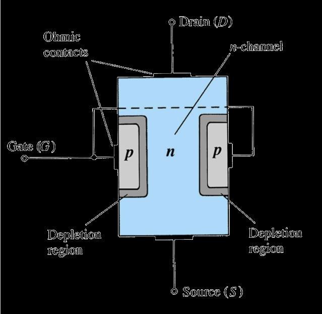
7 7 JFET Structure
8 JFET Operation 8 V GS = 0, V DS >0 increase gradually, I D increases and then saturates
9 JFET Operation 9 V GS = 0, V DS = V P, I D = I DSS V P : pinch off voltage (pinch-off) I D = I DSS (1 - V GS /V P ) 2

10 JFET Operation 10 V GS < 0, V DS > 0, Saturation current reduces when V GS V pinch-off V GS = V P, I D = 0
11 JFET Characteristic Curves 11 I D = f(v GS ) Shockley equation: I G 0A (gate current) I D = I DSS (1 - V GS /V P ) 2 I D = I S (I D drain current, I S source current)


12 JFET Characteristic Curves 12 N-channel, I DSS = 8mA, V P = - 4V P-channel, I DSS = 6mA, V P = 6V
13 13 JFET Symbol

14 JFET 14 2N5457
15 Datasheet-2N Rating Symbol Value Unit Drain-Source voltage V DS 25 Vdc Drain-Gate voltage V DG 25 Vdc Reverse G-S voltage V GSR -25 Vdc Gate current I G 10 nadc Device dissipation 25 0 C Derate above 25 0 C P D mw mw/ 0 C Junction temp range T J C Storage channel temp range T stg -60 to C
16 Datasheet-2N5457-characteristics 16 Characteristic Symbol Min Typ Max Unit V G-S breakdown V (BR)GSS -25 Vdc I gate reverse(vgs=-15, Vds=0) I GSS -1.0 nadc V G-S cutoff V GS(off) Vdc V G-S V GS Vdc I D-zero gate volage I DSS madc C in C iss pf C reverse transfer C rss pf
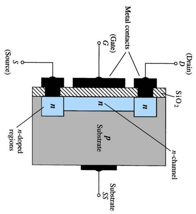
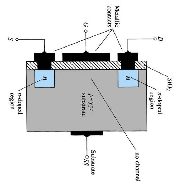
17 MOSFET 17 Structures Operation Characteristic Curves


18 MOSFET Structure 18 N-channel Depletion DMOS N-channel Enhancement EMOS


19 MOSFET Operation 19 N-channel DMOS V GS = 0, V DS > 0 N-channel EMOS V GS > V TH, V DS > 0
20 DMOS Transfer characteristic curves 20 Similar to JFET, transfer characteristic curve I D = f(v GS ) follows Shockley equation: I D = I DSS (1 - V GS /V P ) 2 Can work at: V GS > 0, I D > 0
21 EMOS Transfer characteristic curve 21 Transfer characteristic curve: I D = k(v GS V T ) 2 with V T > 0 (for NMOS) and Vt< 0 for PMOS) When V GS < V T, I D = 0
22 MOSFET Transfer characteristic curve 22 P-channel depletion
23 MOSFET Transfer characteristic curve 23 P-channel enhancement

24 MOSFET Symbol 24 DMOS EMOS

25 25 EMOS 2N4351
26 Datasheet-2N4351-EMOS 26 Characteristic Symbol Min Max Unit V DS breakdown V (BR)DSX 25 Vdc I D-zero gate volage, Vds=10V,Vgs=0, 25C 150C I DSS 10 nadc 10 µadc I gate reverse(vgs=+-15, Vds=0) I GSS +-10 nadc V DS on Voltage V DS(on) 1.0 V C in(vds=10v,id=2ma,f=140khz) C iss 5.0 pf C DS(Vdsub=10V,f=140KHz) C rss 5.0 pf R DS(Vgs=10V,Id=0,f=1KHz) R ds(on) 300 ohms

27 VMOS 27 VMOS Vertical MOSFET, increase channel lenght Increase drain current thanks to large space of heat release High switching speed

28 CMOS 28 CMOS=Complementary MOSFET pmos và nmos: fabricated on same wafer Reduce size and power consumption, increase switching speed Analog/Digital IC design
29 29 Resume JFET DFET MOSFET
30 Biasing types 30 Fixed bias Self-biasing Voltage divider biasing Feedback biasing
31 Some noted 31 With all kinds of FET: I G = 0A I D = I S For JFET & D-MOSFET: I D = I DSS (1 V GS /V P ) 2 For E-MOSFET (MOSFET): I D = k(v GS V T ) 2 (saturation mode) Determine Q-point (DC operating point) and DC load line
 2 V G is fixed at V")
32 Fix biasing (ex: JFET) 32 I G = 0A V S = 0 V GS = V G = - V GG I D = I DSS (1-V GS /V p ) 2 V G is fixed at V GG

33 Fix biasing 33 I D = I DSS (1-V GS /V P ) 2 Build transfer characteristic curve from this table: V GS I D 0 I DSS 0.3V P I DSS /2 0.5Vp I DSS /4 V P 0mA DC load line: V GS = - V GG Intersection between DC load line and trans. Charact. Curve Q point
34 Temperature effect 34 Leakage current I GSS increases when t0 increases cannot neglect RG at mentioned previously so: Q will move from : new Q-point V GS = V GG + I GSS *R G
35 Impact of temperature 35 Question: If V GG =-1V& R G =1 MΩ. I GSS =1nA at 25 C and increase double when temperature increases 10 o C. Determine V GS at 125 o C?
36 Impact of temperature 36 Question: If V GG =-1V& R G =1 MΩ. I GSS =1nA at 25 C and increase double when temperature increases 10 o C. Determine V GS at 125 o C? Answer: At 25 o C, I GSS R G = = 1mV, can be neglected when compare with V GG = - 1V (or new V GS = -999mV). new Q-point When Temp. increases to 125 o C, current I GSS increases to 2 10 times ( 10 3 ) I GSS = nA =1µA I GSS R G =1µA* 1MOhm = 1V New Q point: V GS = 0V & I D = I DSS Q point at C is shifted to a new point and it is far from the initial Q point at room temperature

37 Self biasing 38 What is the main difference compared to fixed biasing? Role of R S? Remove R G to reduce impact of temperature?
38 Self-biasing 39 Loop at input: I G = 0 => V G = 0V V GS = - I S R S (1) I D = I DSS (1-V GS /V p ) 2 (2) To determine Q point: Sole the equation system: (1) + (2) Or by using curve method as shown in the paragraph (intersection point) Consider the impact of Temp.?
39 Voltage divider biasing (ex: JFET) 40 I G = 0, output current I D is controlled by V GS This biasing method is usually used for FET
 2, (2) To determine Q point: Sole the equation system: (1)+(2) Or by using curve method as shown in the paragraph (intersection")
40 Voltage divider biasing (ex: JFET) 41 V G = V DD R 2 /(R 1 +R 2 ) DC load line is: V GS = V G - I D R S (1) R S varies shift of Q point and DC load line Characteristic curve of FET I D = I DSS (1-V GS /V P ) 2, (2) To determine Q point: Sole the equation system: (1)+(2) Or by using curve method as shown in the paragraph (intersection point)
41 Voltage divider biasing (ex: DMOSFET) 42 V G = V DD * 10MΩ/(110MΩ+10MΩ) DC load line: V GS = V G I S *750Ω (1) I D current of DMOS: I D = I DSS (1-V GS /V P ) 2 (2) To determine Q point: Sole the equation system: (1) + (2) Or by using curve method as shown in the paragraph (intersection point)
42 Voltage divider biasing (ex: DMOSFET) 43 With DMOS: I D = I DSS (1-V GS /V P ) 2 V GS can be positive
43 Voltage divider biasing (E-MOSFET) 44 With EMOS: I D = k(v GS -V T ) 2 k=i Don /(V GSon -V T ) 2
44 Voltage divider biasing (ex: E-MOSFET) 45 With EMOS: I D = k(v GS -V T ) 2 where k = I D-on /(V GSon -V T ) 2 Draw transfer characteristic curve of E-MOSFET
45 Feedback biasing (ex: E-MOSFET) 46 At the node G: I G = 0 V G = V D
46 Feedback biasing (ex: E-MOSFET) 47 At the node G: I G = 0 => V G = V D DC load line V GS = V DS = V DD - R D I D (1) Transfer char. equation: I D = k(v GS - V T ) 2, (2) k = I Don /(V GSon -V T ) 2 Solve equ. Sys. (1,2) or use paragraph method

 point Q of")
47 Example 48 Question: Determine Q (I D, V GS ) point Q of these circuits?

 point Q of")
48 Example 49 Question: Determine Q (I D, V GS ) point Q of these circuits?
49 Example 50 Question: Determine V GS and V DS for the E-MOSFET circuit above. Given that this MOSFET has minimum values of I D(on) = 200 ma at V GS = 4V and V th = 2V. Question: Determine I D with V th = 3V.
50 51 Analyze the circuit for AC signal (small signal)

51 52 Small signal model
52 Transconductance 53 g m = I D / V GS = d(i D (V GS )) Derivation of current I D as function of V GS Slope of I D (V GS ) at Q point
53 Transconductance g m (JFET & DMOS) 54 For E-MOS; gm is defined from Shockley equation: g m 2I V DSS P 1 V V GS P When V GS = 0: g m determined at Q point: g g m m0 g 2I V m0 DSS P V 1 V GS P
54 Transconductance g m (E-MOSFET) 55 For JFET & DMOS, gm is defined from: g m determined at Q point:

55 AC equivalent circuit (EMOS) 56 Notes: V GS should be positive for NMOS and negative for PMOS g m = 2k(V GS V T )
56 3 types of MOSFET amplifier 57 CS CD - CG
 Vin")

57 58 EMOS CS with fixed bias voltage VDD Input at G terminal, output at D terminal Common Source RD Vout Fixed biasing (S grounded) Vin Cin RG Cout N-EMOS To draw AC equivalent circuit Short circuit all capacitors + V1 10V Short circuit power supply AC equivalent circuit
 - g m R D if r d > 10R D Input and output voltage are out of phase")
58 59 EMOS CS with fixed bias voltage Z i = R G Z o = r d //R D R D if r d > 10R D A V = - g m (r D //R D ) - g m R D if r d > 10R D Input and output voltage are out of phase
59 60 EMOS CS with voltage divider Input at G terminal, output at D terminal Common Source Voltage divider S terminal is connected to Rs and Cs in parralel Vin C1 1uF R1 G R2 D S VDD RD Vout Cout N-EMOS RS Cs AC equivalent circuit
60 61 EMOS CS with voltage divider Z i = R 1 // R 2 Z o = r d //R D R D nếu r d > 10R D A V = -g m (r D //R D ) g m R D nếu r d > 10R D Input and output voltage are out of phase
61 EMOS CS with voltage divider and wo. Cs 62 Input at G terminal, output at D terminal Common Source Voltage divider S terminal is connected to ONLY Rs and REMOVE bypass-capacitor C S Vin C1 1uF R1 G R2 D S VDD RD Cout N-EMOS RS X Vout Cs????? AC equivalent circuit
62 EMOS CS with voltage divider and wo. Cs 63 Input at G terminal, output at D terminal Common Source Voltage divider S terminal is connected to ONLY Rs and REMOVE bypass-capacitor C S Vin C1 1uF R1 G R2 D S VDD RD Vout Cout N-EMOS RS X Cs AC equivalent circuit
63 EMOS CS with voltage divider and wo. Cs 64 Z i = R G (or R1//R2) Z o = R D /[1+g m R S +(R D +R S )/r d ] A V = -g m R D /[1+g m R S +(R D +R S )/r d ] Input and output voltage are out of phase
64 EMOS CS with feedback bias 65 Input at G terminal, output at D terminal: Common Source Feedback biasing To draw AC equivalent circuit Short circuit all capacitors Short circuit power supply

65 EMOS CS with feedback bias 66 AC equivalent circuit Short circuit all capacitors Short circuit power supply
66 EMOS CS with feedback bias 67 Z i = (R F +r d //R D )/[1+g m (r d //R D )] R F /(1+g m R D ) with r d >10R D, R F >>r d //R D Z o = R F //r d //R D R D with r d >10R D, R F >>r d //R D A V = g m R F //r d //R D g m R D with r d >10R D, R F >>r d //R D Output and input voltage are out of phase

67 68 EMOS CS with feedback bias
68 69 EMOS CS with feedback bias

69 70 EMOS CS with feedback bias
70 JFET CD with fixed biasing 71 Input at G terminal, output at S terminal: Common Drain Fixed biasing
/[1+g m (r d //R S )] g m R S /[1+g m R S )] if r d > 10R S 1 if g m R S >> 1")
71 JFET CD with fixed biasing 72 Z i = R G Z o = r d //R S //(1/g m ) R S //(1/g m ) if r d > 10R S A V = -g m (r d //R S )/[1+g m (r d //R S )] g m R S /[1+g m R S )] if r d > 10R S 1 if g m R S >> 1
72 73 JFET CG with fixed biasing Input at S terminal, output at D terminal: Common GATE Fixed biasing
![74 JFET CG with fixed biasing Z i = R s //[(r d +R D )/(1+g m r d )] R S //(1/g m ) nếu r d >10R D Z o = r d //R D R D](/docs-images/76/74000984/images/73-0.jpg "nếu r d >10R D A V = [g m R D + (R D /r d )]/[1+ R D /r d ] g m R D nếu r d >10R D Input and output voltage are")
73 74 JFET CG with fixed biasing Z i = R s //[(r d +R D )/(1+g m r d )] R S //(1/g m ) nếu r d >10R D Z o = r d //R D R D nếu r d >10R D A V = [g m R D + (R D /r d )]/[1+ R D /r d ] g m R D nếu r d >10R D Input and output voltage are IN-PHASE

74 Equivalent circuit for DMOS 76 Similar to JFET and E-MOSFET For DMOS: V GS can be positive for Nchannel and negative for P channel g m can be higher than g m0
75 77 Resume
76 78 Resume
77 Exercises 79 Chapter 5: 3, 5, 6, 9, 26, 34, 37 Chapter 6: 1, 6, 12, 17, 19, 21, 23 Chapter 9: 1, 5, 12, 17, 19, 23, 27, 32, 33, 37, 38, 43, 44
Chapter7. FET Biasing
 Chapter7. J configurations Fixed biasing Self biasing & Common Gate Voltage divider MOS configurations Depletion-type Enhancement-type JFET: Fixed Biasing Example 7.1: As shown in the figure, it is the
Chapter 6: Field-Effect Transistors
 Chapter 6: Field-Effect Transistors slamic University of Gaza Dr. Talal Skaik FETs vs. BJTs Similarities: Amplifiers Switching devices mpedance matching circuits Differences: FETs are voltage controlled
Monolithic N-Channel JFET Duals
 Monolithic N-Channel JFET Duals N96/97/98/99 Part Number V GS(off) (V) V (BR)GSS Min (V) Min (ms) I G Max (pa) V GS V GS Max (mv) N96.7 to N97.7 to N98.7 to N99.7 to Monolithic Design High Slew Rate Low
Lecture 11: J-FET and MOSFET
 ENE 311 Lecture 11: J-FET and MOSFET FETs vs. BJTs Similarities: Amplifiers Switching devices Impedance matching circuits Differences: FETs are voltage controlled devices. BJTs are current controlled devices.
Monolithic N-Channel JFET Dual
 N9 Monolithic N-Channel JFET Dual V GS(off) (V) V (BR)GSS Min (V) g fs Min (ms) I G Max (pa) V GS V GS Max (mv). to. Monolithic Design High Slew Rate Low Offset/Drift Voltage Low Gate Leakage: pa Low Noise:
Chapter 13 Small-Signal Modeling and Linear Amplification
 Chapter 13 Small-Signal Modeling and Linear Amplification Microelectronic Circuit Design Richard C. Jaeger Travis N. Blalock 1/4/12 Chap 13-1 Chapter Goals Understanding of concepts related to: Transistors
2N5545/46/47/JANTX/JANTXV
 N//7/JANTX/JANTXV Monolithic N-Channel JFET Duals Product Summary Part Number V GS(off) (V) V (BR)GSS Min (V) g fs Min (ms) I G Max (pa) V GS V GS Max (mv) N. to.. N. to.. N7. to.. Features Benefits Applications
Chapter 4 Field-Effect Transistors
 Chapter 4 Field-Effect Transistors Microelectronic Circuit Design Richard C. Jaeger Travis N. Blalock 5/5/11 Chap 4-1 Chapter Goals Describe operation of MOSFETs. Define FET characteristics in operation
J/SST111 Series. N-Channel JFETs. Vishay Siliconix J111 SST111 J112 SST112 J113 SST113
 N-Channel JFETs J SST J SST J SST Part Number V GS(off) (V) r DS(on) Max ( ) I D(off) Typ (pa) t ON Typ (ns) J/SST to 5 4 J/SST to 5 5 5 4 J/SST 5 4 Low On-Resistance: < Fast Switching t ON : 4 ns Low
Chapter 3. FET Amplifiers. Spring th Semester Mechatronics SZABIST, Karachi. Course Support
 Chapter 3 Spring 2012 4 th Semester Mechatronics SZABIST, Karachi 2 Course Support humera.rafique@szabist.edu.pk Office: 100 Campus (404) Official: ZABdesk https://sites.google.com/site/zabistmechatronics/home/spring-2012/ecd
Electronic Circuits 1. Transistor Devices. Contents BJT and FET Characteristics Operations. Prof. C.K. Tse: Transistor devices
 Electronic Circuits 1 Transistor Devices Contents BJT and FET Characteristics Operations 1 What is a transistor? Three-terminal device whose voltage-current relationship is controlled by a third voltage
2SJ280(L), 2SJ280(S)
, 2SJ280(S)") Silicon P-Channel MOS FET November 1996 Application High speed power switching Features Low on-resistance High speed switching Low drive current 4 V gate drive device can be driven from 5 V source Suitable
Silicon P-Channel MOS FET November 1996 Application High speed power switching Features Low on-resistance High speed switching Low drive current 4 V gate drive device can be driven from 5 V source Suitable
Monolithic N-Channel JFET Dual
 SST Monolithic N-Channel JFET Dual V GS(off) (V) V (BR)GSS Min (V) Min (ms) I G Typ (pa) V GS V GS Max (mv) to 6. Monolithic Design High Slew Rate Low Offset/Drift Voltage Low Gate Leakage: pa Low Noise
N-Channel Enhancement-Mode Vertical DMOS FET
 N-Channel Enhancement-Mode Vertical DMOS FET Features Free from secondary breakdown Low power drive requirement Ease of paralleling Low C ISS and fast switching speeds Excellent thermal stability Integral
Monolithic N-Channel JFET Dual
 N98 Monolithic N-Channel JFET Dual V GS(off) (V) V (BR)GSS Min (V) g fs Min (ms) I G Max (pa) V GS V GS Max (mv). to. Monolithic Design High Slew Rate Low Offset/Drift Voltage Low Gate Leakage: pa Low
Lecture 13 MOSFET as an amplifier with an introduction to MOSFET small-signal model and small-signal schematics. Lena Peterson
 Lecture 13 MOSFET as an amplifier with an introduction to MOSFET small-signal model and small-signal schematics Lena Peterson 2015-10-13 Outline (1) Why is the CMOS inverter gain not infinite? Large-signal
Vidyalankar S.E. Sem. III [EXTC] Analog Electronics - I Prelim Question Paper Solution
![Vidyalankar S.E. Sem. III [EXTC] Analog Electronics - I Prelim Question Paper Solution](/thumbs/90/101612294.jpg "Vidyalankar S.E. Sem. III [EXTC] Analog Electronics - I Prelim Question Paper Solution") . (a) S.E. Sem. [EXTC] Analog Electronics - Prelim Question Paper Solution Comparison between BJT and JFET BJT JFET ) BJT is a bipolar device, both majority JFET is an unipolar device, electron and minority
. (a) S.E. Sem. [EXTC] Analog Electronics - Prelim Question Paper Solution Comparison between BJT and JFET BJT JFET ) BJT is a bipolar device, both majority JFET is an unipolar device, electron and minority
2SJ332(L), 2SJ332(S)
, 2SJ332(S)") Silicon P-Channel MOS FET November 1996 Application High speed power switching Features Low on-resistance High speed switching Low drive current 4 V gate drive device can be driven from V source Suitable
Silicon P-Channel MOS FET November 1996 Application High speed power switching Features Low on-resistance High speed switching Low drive current 4 V gate drive device can be driven from V source Suitable
ECE 523/421 - Analog Electronics University of New Mexico Solutions Homework 3
 ECE 523/42 - Analog Electronics University of New Mexico Solutions Homework 3 Problem 7.90 Show that when ro is taken into account, the voltage gain of the source follower becomes G v v o v sig R L r o
2SJ182(L), 2SJ182(S)
, 2SJ182(S)") Silicon P-Channel MOS FET November 1996 Application High speed power switching Features Low on-resistance High speed switching Low drive current 4 V gate drive device Can be driven from V source Suitable
Silicon P-Channel MOS FET November 1996 Application High speed power switching Features Low on-resistance High speed switching Low drive current 4 V gate drive device Can be driven from V source Suitable
PINNING - SOT404 PIN CONFIGURATION SYMBOL
 GENERAL DESCRIPTION QUICK REFERENCE DATA N-channel enhancement mode SYMBOL PARAMETER MAX. UNIT standard level field-effect power transistor in a plastic envelope V DS Drain-source voltage 55 V suitable
Monolithic N-Channel JFET Dual
 New Product SST9NL/U9NL Monolithic N-Channel JFET Dual PRODUCT SUMMARY V GS(off) (V) V (BR)GSS Min (V) g fs Min (ms) I G Max (pa) V GS - V GS Max (mv) -. to -. - - FEATURES BENEFITS APPLICATIONS Anti Latchup
SIPMOS Small-Signal Transistor BSP 149
 SIPMOS Small-Signal Transistor DS 200 I D 0.48 A R DS(on) 3.5 Ω N channel Depletion mode High dynamic resistance Available grouped in GS(th) Type Ordering Tape and Reel Information Pin Configuration Marking
PINNING - TO220AB PIN CONFIGURATION SYMBOL. tab
 BUK958-55 GENERAL DESCRIPTION QUICK REFERENCE DATA N-channel enhancement mode logic SYMBOL PARAMETER MAX. UNIT level field-effect power transistor in a plastic envelope using trench V DS Drain-source voltage
Matched N-Channel JFET Pairs
 Matched N-Channel JFET Pairs N// PRODUCT SUMMARY Part Number V GS(off) (V) V (BR)GSS Min (V) g fs Min I G Typ (pa) V GS V GS Max (mv) N. to 7. N. to 7. N. to 7. FEATURES BENEFITS APPLICATIONS Two-Chip
TO-247-3L Inner Circuit Product Summary I C) R DS(on)
 R DS(on)") Silicon Carbide Power MOSFET N-CHANNEL ENHANCEMENT MODE TO-247-3L Inner Circuit Product Summary V DS I D(@25 C) R DS(on) 1200V 20A 120mΩ Features u Low On-Resistance u Low Capacitance u Avalanche Ruggedness
Silicon Carbide Power MOSFET N-CHANNEL ENHANCEMENT MODE TO-247-3L Inner Circuit Product Summary V DS I D(@25 C) R DS(on) 1200V 20A 120mΩ Features u Low On-Resistance u Low Capacitance u Avalanche Ruggedness
Monolithic N-Channel JFET Dual
 N98 Monolithic N-Channel JFET Dual V GS(off) (V) V (BR)GSS Min (V) g fs Min (ms) I G Max (pa) V GS V GS Max (mv). to. Monolithic Design High Slew Rate Low Offset/Drift Voltage Low Gate Leakage: pa Low
AOT404 N-Channel Enhancement Mode Field Effect Transistor
 AOT44 N-Channel Enhancement Mode Field Effect Transistor General Description The AOT44 uses advanced trench technology and design to provide excellent R DS(ON) with low gate charge. This device is suitable
6.012 Electronic Devices and Circuits Spring 2005
 6.012 Electronic Devices and Circuits Spring 2005 May 16, 2005 Final Exam (200 points) -OPEN BOOK- Problem NAME RECITATION TIME 1 2 3 4 5 Total General guidelines (please read carefully before starting):
N- & P-Channel Enhancement Mode Field Effect Transistor
 PRODUCT SUMMARY V (BR)DSS R DS(ON) I D annel 30 27.5m 7A annel -30 34m -6A G : GATE D : DRAIN S : SOURCE ABSOLUTE MAXIMUM RATINGS (T C = 25 C Unless Otherwise Noted) PARAMETERS/TEST CONDITIONS SYMBOL annel
AON4605 Complementary Enhancement Mode Field Effect Transistor
 AON5 Complementary Enhancement Mode Field Effect Transistor General Description The AON5 uses advanced trench technology to provide excellent R DS(ON) and low gate charge. The complementary MOSFETs form
Matched N-Channel JFET Pairs
 Matched N-Channel JFET Pairs N// PRODUCT SUMMARY Part Number V GS(off) (V) V (BR)GSS Min (V) g fs Min I G Typ (pa) V GS V GS Max (mv) N. to 7. N. to 7. N. to 7. FEATURES BENEFITS APPLICATIONS Two-Chip
DATA SHEET. PMBFJ308; PMBFJ309; PMBFJ310 N-channel silicon field-effect transistors DISCRETE SEMICONDUCTORS
 DISCRETE SEMICONDUCTORS DATA SHEET N-channel silicon field-effect transistors Supersedes data of April 995 File under Discrete Semiconductors, SC7 996 Sep FEATURES Low noise Interchangeability of drain
Features. Symbol Parameter Rating Units V DS Drain-Source Voltage 30 V V GS Gate-Source Voltage ±20 V
 General Description These N-Channel enhancement mode power field effect transistors are using trench DMOS technology. This advanced technology has been especially tailored to minimize on-state resistance,
TOSHIBA Field Effect Transistor Silicon N Channel MOS Type (π MOSIII) 2SK2610
 2SK2610") TOSHIBA Field Effect Transistor Silicon N Channel MOS Type (π MOSIII) Chopper Regulator, DC DC Converter and Motor Drive Applications Unit: mm Low drain source ON resistance : RDS (ON) = 2.3 Ω (typ.) High
TOSHIBA Field Effect Transistor Silicon N Channel MOS Type (π MOSIII) Chopper Regulator, DC DC Converter and Motor Drive Applications Unit: mm Low drain source ON resistance : RDS (ON) = 2.3 Ω (typ.) High
Lecture 3: CMOS Transistor Theory
 Lecture 3: CMOS Transistor Theory Outline Introduction MOS Capacitor nmos I-V Characteristics pmos I-V Characteristics Gate and Diffusion Capacitance 2 Introduction So far, we have treated transistors
500V N-Channel MOSFET
 830 / 830 500V N-Channel MOSFET General Description This Power MOSFET is produced using SL semi s advanced planar stripe DMOS technology. This advanced technology has been especially tailored to minimize
CCS050M12CM2 1.2kV, 50A Silicon Carbide Six-Pack (Three Phase) Module Z-FET TM MOSFET and Z-Rec TM Diode
 Module Z-FET TM MOSFET and Z-Rec TM Diode") CCS5M2CM2.2kV, 5A Silicon Carbide Six-Pack (Three Phase) Module Z-FET TM MOSFET and Z-Rec TM Diode Features Ultra Low Loss Zero Reverse Recovery Current Zero Turn-off Tail Current High-Frequency Operation
CCS5M2CM2.2kV, 5A Silicon Carbide Six-Pack (Three Phase) Module Z-FET TM MOSFET and Z-Rec TM Diode Features Ultra Low Loss Zero Reverse Recovery Current Zero Turn-off Tail Current High-Frequency Operation
PINNING - SOT223 PIN CONFIGURATION SYMBOL
 BUK78-55 GENERAL DESCRIPTION QUICK REFERENCE DATA N-channel enhancement mode logic SYMBOL PARAMETER MAX. UNIT level field-effect power transistor in a plastic envelope suitable for surface V DS Drain-source
PINNING - TO220AB PIN CONFIGURATION SYMBOL. tab
 GENERAL DESCRIPTION QUICK REFERENCE DATA N-channel enhancement mode logic SYMBOL PARAMETER MAX. UNIT level field-effect power transistor in a plastic envelope using trench V DS Drain-source voltage 55
FEATURES SYMBOL QUICK REFERENCE DATA. V DSS = 55 V Very low on-state resistance Fast switching
 PHP37N6LT, PHB37N6LT, PHD37N6LT FEATURES SYMBOL QUICK REFERENCE DATA Trench technology d V DSS = 55 V Very low on-state resistance Fast switching I D = 37 A Stable off-state characteristics High thermal
ECE 342 Electronic Circuits. 3. MOS Transistors
 ECE 342 Electronic Circuits 3. MOS Transistors Jose E. Schutt-Aine Electrical & Computer Engineering University of Illinois jschutt@emlab.uiuc.edu 1 NMOS Transistor Typically L = 0.1 to 3 m, W = 0.2 to
P-Channel Enhancement Mode Mosfet
 WPM34 WPM34 P-Channel Enhancement Mode Mosfet Http://www.sh-willsemi.com Features Higher Efficiency Extending Battery Life Miniature SOT3-3 Surface Mount Package Super high density cell design for extremely
CCS050M12CM2 1.2kV, 25mΩ All-Silicon Carbide Six-Pack (Three Phase) Module C2M MOSFET and Z-Rec TM Diode
 Module C2M MOSFET and Z-Rec TM Diode") CCS5M2CM2.2kV, 25mΩ All-Silicon Carbide Six-Pack (Three Phase) Module C2M MOSFET and Z-Rec TM Diode Features Ultra Low Loss Zero Reverse Recovery Current Zero Turn-off Tail Current High-Frequency Operation
CCS5M2CM2.2kV, 25mΩ All-Silicon Carbide Six-Pack (Three Phase) Module C2M MOSFET and Z-Rec TM Diode Features Ultra Low Loss Zero Reverse Recovery Current Zero Turn-off Tail Current High-Frequency Operation
AO4620 Complementary Enhancement Mode Field Effect Transistor
 AO46 Complementary Enhancement Mode Field Effect Transistor General Description The AO46 uses advanced trench technology MOSFETs to provide excellent and low gate charge. The complementary MOSFETs may
PINNING - TO220AB PIN CONFIGURATION SYMBOL. tab
 BUK755-3A GENERAL DESCRIPTION QUICK REFERENCE DATA N-channel enhancement mode SYMBOL PARAMETER MAX. UNIT standard level field-effect power transistor in a plastic envelope using V DS Drain-source voltage
AON V N-Channel MOSFET
 AON66 V NChannel MOSFET General Description The AON66 utilize advanced trench MOSFET technology in small DFN. x.6 package. This device is ideal for load switch applications. Product Summary V DS V I D
AO7401 P-Channel Enhancement Mode Field Effect Transistor
 Nov P-Channel Enhancement Mode Field Effect Transistor General Description The uses advanced trench technology to provide excellent R DS(ON), low gate charge, and operation with gate voltages as low as.5v,
AON V Common-Drain Dual N-Channel MOSFET
 2V CommonDrain Dual NChannel MOSFET General Description Low R DS(ON) With ESD Protection to improve battery performance and safety Common drain configuration for design simplicity RoHS and HalogenFree
AO3411 P-Channel Enhancement Mode Field Effect Transistor
 January 23 AO3411 P-Channel Enhancement Mode Field Effect Transistor General Description The AO3411 uses advanced trench technology to provide excellent R DS(ON), low gate charge and operation with gate
AOP606 Complementary Enhancement Mode Field Effect Transistor
 AOP66 Complementary Enhancement Mode Field Effect Transistor General Description The AOP66 uses advanced trench technology MOSFETs to provide excellent and low gate charge. The complementary MOSFETs may
P-Channel Enhancement Mode Mosfet
 WPM34 WPM34 P-Channel Enhancement Mode Mosfet Features Higher Efficiency Extending Battery Life Miniature SOT3-3 Surface Mount Package Super high density cell design for extremely low RDS (ON) http://www.willsemi.com
1. (50 points, BJT curves & equivalent) For the 2N3904 =(npn) and the 2N3906 =(pnp)
 For the 2N3904 =(npn) and the 2N3906 =(pnp)") HW 3 1. (50 points, BJT curves & equivalent) For the 2N3904 =(npn) and the 2N3906 =(pnp) a) Obtain in Spice the transistor curves given on the course web page except do in separate plots, one for the npn
HW 3 1. (50 points, BJT curves & equivalent) For the 2N3904 =(npn) and the 2N3906 =(pnp) a) Obtain in Spice the transistor curves given on the course web page except do in separate plots, one for the npn
MMBF4391LT1, MMBF4392LT1, MMBF4393LT1. JFET Switching Transistors. N Channel. Pb Free Packages are Available.
 LT1, LT1, LT1 JFET Switching Transistors NChannel Features PbFree Packages are Available MAXIMUM RATINGS Rating Symbol Value Unit DrainSource Voltage V DS Vdc DrainGate Voltage V DG Vdc GateSource Voltage
1.2 kv 16 mω 1.8 mj. Package. Symbol Parameter Value Unit Test Conditions Notes 117 V GS = 20V, T C
 CAS1H12AM1 1.2 kv, 1A Silicon Carbide Half-Bridge Module Z-FET TM MOSFET and Z-Rec TM Diode Not recommended for new designs. Replacement part: CAS12M12BM2 Features Ultra Low Loss Zero Turn-off Tail Current
FEATURES SYMBOL QUICK REFERENCE DATA
 FEATURES SYMBOL QUICK REFERENCE DATA Trench technology Low on-state resistance Fast switching d g s V DSS = 2 V I D = 7.6 A R DS(ON) 23 mω GENERAL DESCRIPTION N-channel enhancement mode field-effect power
JFET Operating Characteristics: V GS = 0 V 14. JFET Operating Characteristics: V GS = 0 V 15
 J Operating Characteristics: V GS = 0 V 14 V GS = 0 and V DS increases from 0 to a more positive voltage: Gate and Source terminals: at the same potential Drain: at positive potential => reverse biased
CCS050M12CM2 1.2kV, 50A Silicon Carbide Six-Pack (Three Phase) Module Z-FET TM MOSFET and Z-Rec TM Diode
 Module Z-FET TM MOSFET and Z-Rec TM Diode") CCS5M12CM2 1.2kV, 5A Silicon Carbide Six-Pack (Three Phase) Module Z-FET TM MOSFET and Z-Rec TM Diode Features Ultra Low Loss Zero Reverse Recovery Current Zero Turn-off Tail Current High-Frequency Operation
CCS5M12CM2 1.2kV, 5A Silicon Carbide Six-Pack (Three Phase) Module Z-FET TM MOSFET and Z-Rec TM Diode Features Ultra Low Loss Zero Reverse Recovery Current Zero Turn-off Tail Current High-Frequency Operation
2N4856JAN/JANTX/JANTXV Series. N-Channel JFETs. Vishay Siliconix
 N-Channel JFETs 2N4856JAN 2N4856JANTX 2N4856JANTX 2N4857JAN 2N4857JANTX 2N4857JANTX 2N4858JAN 2N4858JANTX 2N4858JANTX 2N4859JAN 2N4859JANTX 2N4859JANTX 2N4860JAN 2N4860JANTX 2N4860JANTX 2N4861JAN 2N4861JANTX
N-Channel Enhancement-Mode Vertical DMOS FETs
 VN16 N-Channel Enhancement-Mode Vertical DMOS FETs Features Free from secondary breakdown Low power drive requirement Ease of paralleling Low C ISS and fast switching speeds High input impedance and high
EE105 Fall 2014 Microelectronic Devices and Circuits. NMOS Transistor Capacitances: Saturation Region
 EE105 Fall 014 Microelectronic Devices and Circuits Prof. Ming C. Wu wu@eecs.berkeley.edu 511 Sutardja Dai Hall (SDH) 1 NMOS Transistor Capacitances: Saturation Region Drain no longer connected to channel
P-Channel Enhancement Mode Field Effect Transistor PARAMETERS/TEST CONDITIONS SYMBOL LIMITS UNITS
 PRODUCT SUMMARY D V (BR)DSS R DS(ON) I D -4V 15mΩ -45A G 1. GATE 2. DRAIN 3. SOURCE ABSOLUTE MAXIMUM RATINGS (T A = 25 C Unless Otherwise Noted) PARAMETERS/TEST CONDITIONS SYMBOL LIMITS UNITS Drain-Source
AO4607, AO4607L(Lead-Free) Complementary Enhancement Mode Field Effect Transistor
 Complementary Enhancement Mode Field Effect Transistor") Rev : Feb 3 Rev : Jan 4 AO467, AO467L(Lead-Free) Complementary Enhancement Mode Field Effect Transistor General Description The AO467 uses advanced trench technology MOSFETs to provide excellen R DS(ON)
Rev : Feb 3 Rev : Jan 4 AO467, AO467L(Lead-Free) Complementary Enhancement Mode Field Effect Transistor General Description The AO467 uses advanced trench technology MOSFETs to provide excellen R DS(ON)
Supertex inc. TN0104. N-Channel Enhancement-Mode Vertical DMOS FET. Features. General Description. Applications. Ordering Information.
 TN1 N-Channel Enhancement-Mode Vertical DMOS FET Features Low threshold (1.6V max.) High input impedance Low input capacitance Fast switching speeds Low on-resistance Free from secondary breakdown Low
Features. Symbol Parameter Rating Units V DS Drain-Source Voltage 600 V V GS Gate-Source Voltage ±30 V
 General Description These N-Channel enhancement mode power field effect transistors are planar stripe, DMOS technology. This advanced technology has been especially tailored to minimize on-state resistance,
N-channel TrenchMOS transistor
 PSMN2-5W FEATURES SYMBOL QUICK REFERENCE DATA Trench technology Very low on-state resistance Fast switching Low thermal resistance g d s V DSS = 5 V I D = 73 A R DS(ON) 2 mω GENERAL DESCRIPTION PINNING
P-channel enhancement mode MOS transistor
 FEATURES SYMBOL QUICK REFERENCE DATA Very low threshold voltage s V DS = 2 V Fast switching Logic level compatible I D =.2 A Subminiature surface mount g package R DS(ON). Ω (V GS =. V) GENERAL DESCRIPTION
Max Q1. Symbol V GS I DM 15 I DSM 7.8 I AS E AS V SPIKE P D 2.5 P DSM. Junction and Storage Temperature Range T J, T STG
 3V Dual Asymmetric N-Channel AlphaMOS General Description Latest Trench Power AlphaMOS (αmos LV) technology Very Low RDS(on) at 4.V GS Low Gate Charge High Current Capability RoHS and Halogen-Free Compliant
AOD4184A 40V N-Channel MOSFET
 4V NChannel MOSFET General Description The AOD484A combines advanced trench MOSFET technology with a low resistance package to provide extremely low R DS(ON). This device is well suited for high current
AOD466 N-Channel Enhancement Mode Field Effect Transistor
 NChannel Enhancement Mode Field Effect Transistor General Description The AOD466 uses advanced trench technology and design to provide excellent R DS(ON) with low gate charge. This device is suitable for
TOSHIBA Field Effect Transistor Silicon N Channel MOS Type (π-mosⅦ) TK6A50D
 TK6A50D") TOSHIBA Field Effect Transistor Silicon N Channel MOS Type (π-mosⅦ) TKAD TKAD Switching Regulator Applications Unit: mm Low drain-source ON-resistance: R DS (ON) =. Ω (typ.) High forward transfer admittance:
TOSHIBA Field Effect Transistor Silicon N Channel MOS Type (π-mosⅦ) TKAD TKAD Switching Regulator Applications Unit: mm Low drain-source ON-resistance: R DS (ON) =. Ω (typ.) High forward transfer admittance:
N-Channel Depletion-Mode DMOS FET
 Features Free from secondary breakdown Low power drive requirement Ease of paralleling Excellent thermal stability Integral source-drain diode High input impedance and low C ISS ESD gate protection Applications
DISCRETE SEMICONDUCTORS DATA SHEET. BLF245 VHF power MOS transistor
 DISCRETE SEMICONDUCTORS DATA SHEET September 1992 FEATURES High power gain Low noise figure Easy power control Good thermal stability Withstands full load mismatch. DESCRIPTION Silicon N-channel enhancement
PINNING - TO220AB PIN CONFIGURATION SYMBOL
 BUK442A/B GENERAL DESCRIPTION QUICK REFERENCE DATA Nchannel enhancement mode SYMBOL PARAMETER MAX. UNIT fieldeffect power transistor in a plastic envelope suitable for use in surface V DS Drainsource voltage
N-Channel Enhancement-Mode Vertical DMOS FET
 N-Channel Enhancement-Mode Vertical DMOS FET Features Free from secondary breakdown Low power drive requirement Ease of paralleling Low C ISS and fast switching speeds Excellent thermal stability Integral
ECE-343 Test 2: Mar 21, :00-8:00, Closed Book. Name : SOLUTION
 ECE-343 Test 2: Mar 21, 2012 6:00-8:00, Closed Book Name : SOLUTION 1. (25 pts) (a) Draw a circuit diagram for a differential amplifier designed under the following constraints: Use only BJTs. (You may
TPC8116-H TPC8116-H. High Efficiency DC/DC Converter Applications Notebook PC Applications Portable Equipment Applications CCFL Inverter Applications
 TOSHIBA Field Effect Transistor Silicon P-Channel MOS Type (Ultra-High-Speed U-MOSIII) High Efficiency DC/DC Converter Applications Notebook PC Applications Portable Equipment Applications CCFL Inverter
PINNING - TO220AB PIN CONFIGURATION SYMBOL
 BUK4552A/B GENERAL DESCRIPTION QUICK REFERENCE DATA Nchannel enhancement mode SYMBOL PARAMETER MAX. MAX. UNIT fieldeffect power transistor in a plastic envelope. BUK455 2A 2B The device is intended for
PINNING - TO220AB PIN CONFIGURATION SYMBOL
 BUK536A/B GENERAL DESCRIPTION QUICK REFERENCE DATA Nchannel enhancement mode SYMBOL PARAMETER MAX. MAX. UNIT fieldeffect power transistor in a plastic envelope. BUK53 6A 6B The device is intended for use
AOP605 Complementary Enhancement Mode Field Effect Transistor
 AOP65 Complementary Enhancement Mode Field Effect Transistor General Description The AOP65/L uses advanced trench technology to provide excellent and low gate charge. The complementary MOSFETs form a highspeed
CPC3730CTR. 350V N-Channel Depletion-Mode FET (SOT-89) INTEGRATED CIRCUITS DIVISION
 INTEGRATED CIRCUITS DIVISION") V (BR)DSX / V (BR)DGX R DS(on) (max) I DSS (min) Package 35V P 3 14mA SOT-89 Features Low R DS(on) at Cold Temperatures R DS(on) 3 max. at 25ºC High Input Impedance High Breakdown Voltage: 35V P Low (off)
V (BR)DSX / V (BR)DGX R DS(on) (max) I DSS (min) Package 35V P 3 14mA SOT-89 Features Low R DS(on) at Cold Temperatures R DS(on) 3 max. at 25ºC High Input Impedance High Breakdown Voltage: 35V P Low (off)
PINNING - SOT223 PIN CONFIGURATION SYMBOL
 BUK86A GENERAL DESCRIPTION QUICK REFERENCE DATA Nchannel enhancement mode SYMBOL PARAMETER MAX. UNIT logic level fieldeffect power transistor in a plastic envelope V DS Drainsource voltage 6 V suitable
BSS84 P-Channel Enhancement Mode Field-Effect Transistor
 BSS8 P-Channel Enhancement Mode Field-Effect Transistor Features -. A, - V, R DS(ON) = Ω at V GS = - V Voltage-Controlled P-Channel Small-Signal Switch High-Density Cell Design for Low R DS(ON) High Saturation
Features. T A =25 o C unless otherwise noted
 NDS65 NDS65 P-Channel Enhancement Mode Field Effect Transistor General Description These P-Channel enhancement mode field effect transistors are produced using ON Semiconductor s proprietary, high cell
AO V Dual N-Channel MOSFET
 AO688 V Dual NChannel MOSFET General Description The AO688 uses advanced trench technology to provide excellent R DS(ON), low gate charge and operation with gate voltages as low as.5v. This device is suitable
PowerMOS transistor PINNING - SOT428 PIN CONFIGURATION SYMBOL. tab
 PHDE GENERAL DESCRIPTION QUICK REFERENCE DATA Nchannel enhancement mode SYMBOL PARAMETER MAX. UNIT fieldeffect power transistor in a plastic envelope suitable for surface V DS Drainsource voltage 6 V mounting
AO V Dual P + N-Channel MOSFET
 4V Dual P + N-Channel MOSFET General Description The AO467 uses advanced trench technology MOSFETs to provide excellent and low gate charge. The complementary MOSFETs may be used in H-bridge, Inverters
TOSHIBA Field-Effect Transistor Silicon P-Channel MOS Type SSM3J117TU. Characteristic Symbol Test Condition Min Typ. Max Unit
 TOSHIBA Field-Effect Transistor Silicon P-Channel MOS Type SSMJ7TU High-Speed Switching Applications 4 V drive Low ON-resistance: R on = 225 mω (max) (@V GS = ) R on = 7 mω (max) (@V GS = V) Absolute Maximum
ECE315 / ECE515 Lecture 11 Date:
 ecture 11 Date: 15.09.016 MOS Differential Pair Quantitative Analysis differential input Small Signal Analysis MOS Differential Pair ECE315 / ECE515 M 1 and M are perfectly matched (at least in theory!)
N-Channel Lateral DMOS FETs
 N-Channel Lateral DMOS FETs (Available Only In Extended Hi-Rel Flow) SDDE-/DE- Part Number V (BR)DS Min (V) V GS(th) Max (V) r DS(on) Max ( ) C rss Max (pf) t ON Max (ns) SDDE-. @ V GS = V. SDDE-. @ V
N-Channel 30-V (D-S) MOSFET With Sense Terminal
 MOSFET With Sense Terminal") SUM5N3-3LC N-Channel 3-V (D-S) MOSFET With Sense Terminal PRODUCT SUMMARY V (BR)DSS (V) r DS(on) ( ) (A).3 @ V S = V 5 a 3.7 @ V S =.5 V a FEATURES TrenchFET Power MOSFET Plus Current Sensing Diode New
SUM5N3-3LC N-Channel 3-V (D-S) MOSFET With Sense Terminal PRODUCT SUMMARY V (BR)DSS (V) r DS(on) ( ) (A).3 @ V S = V 5 a 3.7 @ V S =.5 V a FEATURES TrenchFET Power MOSFET Plus Current Sensing Diode New
Product Summary: BVDSS 30V RDSON (MAX.) 50mΩ 4.5A I D. Pb Free Lead Plating & Halogen Free EMB50P03J
 50mΩ 4.5A I D. Pb Free Lead Plating & Halogen Free EMB50P03J") P Channel Logic Level Enhancement Mode Field Effect Transistor Product Summary: BVDSS V RDSON (MAX.) ID 5mΩ.5A Pb Free Lead Plating & Halogen Free D G S ABSOLUTE MAXIMUM RATINGS (T A = 5 C Unless Otherwise
P Channel Logic Level Enhancement Mode Field Effect Transistor Product Summary: BVDSS V RDSON (MAX.) ID 5mΩ.5A Pb Free Lead Plating & Halogen Free D G S ABSOLUTE MAXIMUM RATINGS (T A = 5 C Unless Otherwise
TSP10N60M / TSF10N60M
 TSP10N60M / TSF10N60M 600V N-Channel MOSFET General Description This Power MOSFET is produced using Truesemi s advanced planar stripe DMOS technology. This advanced technology has been especially tailored
IRF5851. HEXFET Power MOSFET. Ultra Low On-Resistance Dual N and P Channel MOSFET Surface Mount Available in Tape & Reel Low Gate Charge.
 PD-93998B HEXFET Power MOSFET l l l l l Ultra Low On-Resistance Dual N and P Channel MOSFET Surface Mount Available in Tape & Reel Low Gate Charge G S2 G2 2 3 6 5 4 D S D2 N-Ch P-Ch DSS 20-20 R DS(on)
GP1M003A080H/ GP1M003A080F GP1M003A080HH/ GP1M003A080FH
 Features Low gate charge 1% avalanche tested Improved dv/dt capability RoHS compliant Halogen free package JEDEC Qualification S = 88 V @T jmax = 3A R DS(ON) =. (max) @ = 1 V D G Absolute Maximum Ratings
TO220AB & SOT404 PIN CONFIGURATION SYMBOL
 BUK754-55A BUK764-55A GENERAL DESCRIPTION QUICK REFERENCE DATA N-channel enhancement mode SYMBOL PARAMETER MAX. UNIT standard level field-effect power transistor in a plastic envelope V DS Drain-source
Type V DS I D R DS(on) Package Ordering Code BTS V 10 A 0.2 Ω TO-220AB C67078-A5008-A2
 Package Ordering Code BTS V 10 A 0.2 Ω TO-220AB C67078-A5008-A2") TEMPFET Features N channel Enhancement mode Temperature sensor with thyristor characteristic The drain pin is electrically shorted to the tab 1 2 3 Pin 1 2 3 G D S Type V DS I D R DS(on) Package Ordering
TEMPFET Features N channel Enhancement mode Temperature sensor with thyristor characteristic The drain pin is electrically shorted to the tab 1 2 3 Pin 1 2 3 G D S Type V DS I D R DS(on) Package Ordering
PINNING - TO220AB PIN CONFIGURATION SYMBOL
 GENERAL DESCRIPTION QUICK REFERENCE DATA Nchannel enhancement mode SYMBOL PARAMETER MAX. MAX. UNIT fieldeffect power transistor in a plastic envelope. BUK455 A B The device is intended for use in V DS
Biasing the CE Amplifier
 Biasing the CE Amplifier Graphical approach: plot I C as a function of the DC base-emitter voltage (note: normally plot vs. base current, so we must return to Ebers-Moll): I C I S e V BE V th I S e V th
DATA SHEET. BF245A; BF245B; BF245C N-channel silicon field-effect transistors DISCRETE SEMICONDUCTORS
 DISCRETE SEMICONDUCTORS DATA SHEET N-channel silicon field-effect transistors Supersedes data of April 995 File under Discrete Semiconductors, SC7 996 Jul FEATURES Interchangeability of drain and source