TOSHIBA Field Effect Transistor Silicon N Channel MOS Type (π MOSIII) 2SK2610
|
|
|
- Buck Park
- 5 years ago
- Views:
Transcription
1 TOSHIBA Field Effect Transistor Silicon N Channel MOS Type (π MOSIII) Chopper Regulator, DC DC Converter and Motor Drive Applications Unit: mm Low drain source ON resistance : RDS (ON) = 2.3 Ω (typ.) High forward transfer admittance : Yfs = 4.4 S (typ.) Low leakage current : IDSS = 100 µa (max) (VDS = 720 V) Enhancement mode : Vth = 2.0~4.0 V (VDS = 10 V, ID = 1 ma) Absolute Maximum Ratings (Ta = 25 C) Characteristics Symbol Rating Unit Drain source voltage V DSS 900 V Drain gate voltage (R GS = 20 kω) V DGR 900 V Gate source voltage V GSS ±30 V Drain current DC (Note 1) I D 5 A Pulse (Note 1) I DP 15 Drain power dissipation (Tc = 25 C) P D 150 W 1. GATE 2. DRAIN (HEAT SINK) 3. SOURCE Single pulse avalanche energy (Note 2) E AS 595 mj Avalanche current I AR 5 A Repetitive avalanche energy (Note 3) E AR 15 mj JEDEC JEITA TOSHIBA SC C1B Channel temperature T ch 150 C Storage temperature range T stg 55~150 C Weight: 4.6 g (typ.) Note: Using continuously under heavy loads (e.g. the application of high temperature/current/voltage and the significant change in temperature, etc.) may cause this product to decrease in the reliability significantly even if the operating conditions (i.e. operating temperature/current/voltage, etc.) are within the absolute maximum ratings. Please design the appropriate reliability upon reviewing the Toshiba Semiconductor Reliability Handbook ( Handling Precautions /Derating Concept and Methods) and individual reliability data (i.e. reliability test report and estimated failure rate, etc). Thermal Characteristics Characteristics Symbol Max Unit Thermal resistance, channel to case R th (ch c) C / W Thermal resistance, channel to ambient R th (ch a) 50 C / W Note 1: Ensure that the channel temperature does not exceed 150 C. Note 2: V DD = 90 V, T ch = 25 C (initial), L = 43.6 mh, I AR = 5 A, R G = 25 Ω Note 3: Repetitive rating: pulse width limited by maximum channel temperature This transistor is an electrostatic-sensitive device. Please handle with caution. 1
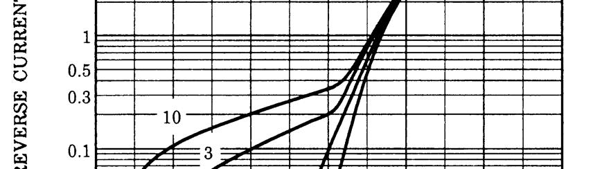
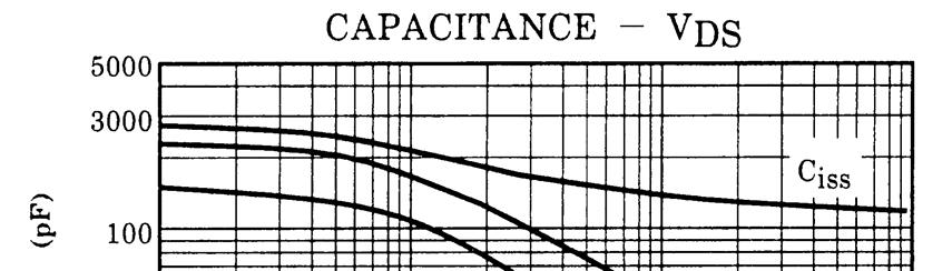
2 Electrical Characteristics (Ta = 25 C) Characteristics Symbol Test Condition Min Typ. Max Unit Gate leakage current I GSS V GS = ±30 V, V DS = 0 V ±10 µa Gate source breakdown voltage V (BR) GSS I G = ±10 µa, V DS = 0 V ±30 V Drain cut off current I DSS V DS = 720 V, V GS = 0 V 100 µa Drain source breakdown voltage V (BR) DSS I D = 10 ma, V GS = 0 V 900 V Gate threshold voltage V th V DS = 10 V, I D = 1 ma V Drain source ON resistance R DS (ON) V GS = 10 V, I D = 3.0 A Ω Forward transfer admittance Y fs V DS = 20 V, I D = 3.0 A S Input capacitance C iss 1200 Reverse transfer capacitance C rss V DS = 25 V, V GS = 0 V, f = 1 MHz 20 pf Output capacitance C oss 120 Rise time t r 40 Switching time Turn on time t on 90 Fall time t f 60 ns Turn off time t off 200 Total gate charge (gate source plus gate drain) Q g 45 Gate source charge Q gs V DD 400 V, V GS = 10 V, I D = 5 A 25 Gate drain ( miller ) Charge Q gd 20 nc Source Drain Ratings and Characteristics (Ta = 25 C) Characteristics Symbol Test Condition Min Typ. Max Unit Continuous drain reverse current (Note 1) Pulse drain reverse current (Note 1) I DR 5 A I DRP 15 A Forward voltage (diode) V DSF I DR = 5 A, V GS = 0 V 1.9 V Reverse recovery time t rr I DR = 5 A, V GS = 0 V, di DR / dt = 100 A / µs 1300 ns Reverse recovery charge Q rr 11 µc Marking TOSHIBA K2610 Part No. (or abbreviation code) Lot No. A line indicates lead (Pb)-free package or lead (Pb)-free finish. 2
3 3
4 4
5 NORMALIZED TRANSIENT THERMAL IMPEDANCE rth (t)/rth (ch-c) R G = 25 Ω V DD = 90 V, L = 43.6 mh 1 BVDSS EAS = L I2 2 BVDSS VDD 5
6 6
TOSHIBA Field Effect Transistor Silicon N Channel MOS Type (π-mosⅦ) TK6A50D
 TK6A50D") TOSHIBA Field Effect Transistor Silicon N Channel MOS Type (π-mosⅦ) TKAD TKAD Switching Regulator Applications Unit: mm Low drain-source ON-resistance: R DS (ON) =. Ω (typ.) High forward transfer admittance:
TOSHIBA Field Effect Transistor Silicon N Channel MOS Type (π-mosⅦ) TKAD TKAD Switching Regulator Applications Unit: mm Low drain-source ON-resistance: R DS (ON) =. Ω (typ.) High forward transfer admittance:
TOSHIBA Field Effect Transistor Silicon N Channel MOS Type (L 2 π MOSV) 2SK2385
 2SK2385") TOSHIBA Field Effect Transistor Silicon N Channel MOS Type (L 2 π MOSV) 2SK2385 2SK2385 Chopper Regulator, DC DC Converter and Motor Drive Applications Unit: mm 4 V gate drive Low drain source ON resistance
TOSHIBA Field Effect Transistor Silicon N Channel MOS Type (L 2 π MOSV) 2SK2385 2SK2385 Chopper Regulator, DC DC Converter and Motor Drive Applications Unit: mm 4 V gate drive Low drain source ON resistance
TOSHIBA Field Effect Transistor Silicon N Channel MOS Type (π-mosvi) 2SK3567
 2SK3567") SK7 TOSHIBA Field Effect Transistor Silicon N Channel MOS Type (π-mosvi) SK7 Switching Regulator Applications Unit: mm Low drain-source ON resistance: RDS (ON) =.7Ω (typ.) High forward transfer admittance:
SK7 TOSHIBA Field Effect Transistor Silicon N Channel MOS Type (π-mosvi) SK7 Switching Regulator Applications Unit: mm Low drain-source ON resistance: RDS (ON) =.7Ω (typ.) High forward transfer admittance:
TOSHIBA Field Effect Transistor Silicon P-Channel MOS Type (U MOSIII) 2SJ668
 2SJ668") TOSHIBA Field Effect Transistor Silicon P-Channel MOS Type (U MOSIII) 2SJ668 Relay Drive, DC/DC Converter and Motor Drive Applications Unit: mm 4 V gate drive Low drain source ON-resistance: R DS (ON)
TOSHIBA Field Effect Transistor Silicon P-Channel MOS Type (U MOSIII) 2SJ668 Relay Drive, DC/DC Converter and Motor Drive Applications Unit: mm 4 V gate drive Low drain source ON-resistance: R DS (ON)
TOSHIBA Field Effect Transistor Silicon N Channel MOS Type (π-mosvi) 2SK3667
 2SK3667") SK7 TOSHIBA Field Effect Transistor Silicon N Channel MOS Type (π-mosvi) SK7 Switching Regulator Applications Unit: mm Low drain-source ON resistance: R DS (ON) =.7Ω (typ.) High forward transfer admittance:
SK7 TOSHIBA Field Effect Transistor Silicon N Channel MOS Type (π-mosvi) SK7 Switching Regulator Applications Unit: mm Low drain-source ON resistance: R DS (ON) =.7Ω (typ.) High forward transfer admittance:
TOSHIBA Field Effect Transistor Silicon N Channel MOS Type (π MOSV) 2SK2996
 2SK2996") TOSHIBA Field Effect Transistor Silicon N Channel MOS Type (π MOSV) 2SK2996 DC DC Converter, Relay Drive and Motor Drive Applications Unit: mm Low drain source ON resistance : RDS (ON) = 0.74 Ω (typ.)
TOSHIBA Field Effect Transistor Silicon N Channel MOS Type (π MOSV) 2SK2996 DC DC Converter, Relay Drive and Motor Drive Applications Unit: mm Low drain source ON resistance : RDS (ON) = 0.74 Ω (typ.)
TOSHIBA Field Effect Transistor Silicon N Channel MOS Type (π-mosⅣ) 2SK4013
 2SK4013") SK TOSHIBA Field Effect Transistor Silicon N Channel MOS Type (π-mosⅣ) SK Switching Regulator Applications Unit: mm Low drain-source ON resistance: RDS (ON) =. Ω (typ.) High forward transfer admittance:
SK TOSHIBA Field Effect Transistor Silicon N Channel MOS Type (π-mosⅣ) SK Switching Regulator Applications Unit: mm Low drain-source ON resistance: RDS (ON) =. Ω (typ.) High forward transfer admittance:
TOSHIBA Field Effect Transistor Silicon N Channel MOS Type (π-mosvi) 2SK3767
 2SK3767") SK77 TOSHIBA Field Effect Transistor Silicon N Channel MOS Type (π-mosvi) SK77 Switching Regulator Applications Unit: mm Low drain-source ON resistance: RDS (ON) =.Ω (typ.) High forward transfer admittance:
SK77 TOSHIBA Field Effect Transistor Silicon N Channel MOS Type (π-mosvi) SK77 Switching Regulator Applications Unit: mm Low drain-source ON resistance: RDS (ON) =.Ω (typ.) High forward transfer admittance:
TOSHIBA Field Effect Transistor Silicon N-Channel MOS Type (π-mos VI) 2SK4108. JEDEC Repetitive avalanche energy (Note 3) E AR 15 mj
 2SK4108. JEDEC Repetitive avalanche energy (Note 3) E AR 15 mj") SK TOSHIBA Field Effect Transistor Silicon N-Channel MOS Type (π-mos VI) SK Switching Regulator Applications Unit: mm Low drain source ON resistance : R DS (ON) =. Ω (typ.) High forward transfer admittance
SK TOSHIBA Field Effect Transistor Silicon N-Channel MOS Type (π-mos VI) SK Switching Regulator Applications Unit: mm Low drain source ON resistance : R DS (ON) =. Ω (typ.) High forward transfer admittance
TPC8116-H TPC8116-H. High Efficiency DC/DC Converter Applications Notebook PC Applications Portable Equipment Applications CCFL Inverter Applications
 TOSHIBA Field Effect Transistor Silicon P-Channel MOS Type (Ultra-High-Speed U-MOSIII) High Efficiency DC/DC Converter Applications Notebook PC Applications Portable Equipment Applications CCFL Inverter
TOSHIBA Field Effect Transistor Silicon N Channel MOS Type (π-mosiv) 2SK3565
 2SK3565") SK TOSHIBA Field Effect Transistor Silicon N Channel MOS Type (π-mosiv) SK Switching Regulator Applications Unit: mm Low drain-source ON resistance: RDS (ON) =.Ω (typ.) High forward transfer admittance:
SK TOSHIBA Field Effect Transistor Silicon N Channel MOS Type (π-mosiv) SK Switching Regulator Applications Unit: mm Low drain-source ON resistance: RDS (ON) =.Ω (typ.) High forward transfer admittance:
TOSHIBA Field Effect Transistor Silicon N Channel MOS Type (DTMOS ) TK15J60U
 TK15J60U") TOSHIBA Field Effect Transistor Silicon N Channel MOS Type (DTMOS ) Switching Regulator Applications Unit: mm Low drain-source ON-resistance: R DS (ON) =. (typ.) High forward transfer admittance: Y fs
TOSHIBA Field Effect Transistor Silicon N Channel MOS Type (DTMOS ) Switching Regulator Applications Unit: mm Low drain-source ON-resistance: R DS (ON) =. (typ.) High forward transfer admittance: Y fs
TOSHIBA Field Effect Transistor Silicon N Channel MOS Type (π-mosⅦ) TK12A50D
 TK12A50D") TOSHIBA Field Effect Transistor Silicon N Channel MOS Type (π-mosⅦ) TKAD TKAD Switching Regulator Applications Unit: mm Low drain-source ON-resistance: R DS (ON) =. Ω (typ.) High forward transfer admittance:
TOSHIBA Field Effect Transistor Silicon N Channel MOS Type (π-mosⅦ) TKAD TKAD Switching Regulator Applications Unit: mm Low drain-source ON-resistance: R DS (ON) =. Ω (typ.) High forward transfer admittance:
TOSHIBA Field Effect Transistor Silicon N Channel MOS Type (U MOSⅢ) TK30A06J3
 TK30A06J3") TOSHIBA Field Effect Transistor Silicon N Channel MOS Type (U MOSⅢ) Motor Drive Application Load Swithch Application Chopper Regulator and DC DC Converter Application Unit: mm Low drain-source ON resistance:
TOSHIBA Field Effect Transistor Silicon N Channel MOS Type (U MOSⅢ) Motor Drive Application Load Swithch Application Chopper Regulator and DC DC Converter Application Unit: mm Low drain-source ON resistance:
TOSHIBA Field Effect Transistor Silicon N Channel MOS Type (DTMOS) TK40J60T
 TK40J60T") TKJT TOSHIBA Field Effect Transistor Silicon N Channel MOS Type (DTMOS) TKJT Switching Regulator Applications Unit: mm Low drain-source ON resistance: R DS (ON) =.Ω (typ.) High forward transfer admittance:
TKJT TOSHIBA Field Effect Transistor Silicon N Channel MOS Type (DTMOS) TKJT Switching Regulator Applications Unit: mm Low drain-source ON resistance: R DS (ON) =.Ω (typ.) High forward transfer admittance:
TOSHIBA Field Effect Transistor Silicon P Channel MOS Type (U-MOS III) TPCF8102
 TPCF8102") TOSHIBA Field Effect Transistor Silicon P Channel MOS Type (U-MOS III) TPCF82 TPCF82 Notebook PC Applications Portable Equipment Applications Unit: mm Low drain-source ON resistance: RDS (ON) = 24 mω (typ.)
TOSHIBA Field Effect Transistor Silicon P Channel MOS Type (U-MOS III) TPCF82 TPCF82 Notebook PC Applications Portable Equipment Applications Unit: mm Low drain-source ON resistance: RDS (ON) = 24 mω (typ.)
TOSHIBA Field Effect Transistor Silicon N Channel MOS Type (U-MOSII) 2SK3236
 2SK3236") TOSHIBA Field Effect Transistor Silicon N Channel MOS Type (U-MOSII) 2SK3236 Switching Regulator Applications, DC-DC Converter and Motor Drive Applications Unit: mm V gate drive Low drain-source ON resistance:
TOSHIBA Field Effect Transistor Silicon N Channel MOS Type (U-MOSII) 2SK3236 Switching Regulator Applications, DC-DC Converter and Motor Drive Applications Unit: mm V gate drive Low drain-source ON resistance:
TOSHIBA Field Effect Transistor Silicon N Channel MOS Type (π-mosv) 2SK3538
 2SK3538") SK TOSHIBA Field Effect Transistor Silicon N Channel MOS Type (π-mosv) SK Switching Regulator, DC-DC Converter Applications Unit: mm Low drain-source ON resistance: RDS (ON) = 7 mω (typ.) High forward
SK TOSHIBA Field Effect Transistor Silicon N Channel MOS Type (π-mosv) SK Switching Regulator, DC-DC Converter Applications Unit: mm Low drain-source ON resistance: RDS (ON) = 7 mω (typ.) High forward
TOSHIBA Field Effect Transistor Silicon N Channel MOS Type (U-MOSIII) TPC6004
 TPC6004") TPC TOSHIBA Field Effect Transistor Silicon N Channel MOS Type (U-MOSIII) TPC Notebook PC Applications Portable Equipment Applications Unit: mm Low drain-source ON resistance: R DS (ON) = 9 mω (typ.) High
TPC TOSHIBA Field Effect Transistor Silicon N Channel MOS Type (U-MOSIII) TPC Notebook PC Applications Portable Equipment Applications Unit: mm Low drain-source ON resistance: R DS (ON) = 9 mω (typ.) High
TOSHIBA Field Effect Transistor Silicon P Channel MOS Type (U-MOSⅣ) TPC8114. DC (Note 1) I D 18 A Pulse (Note 1) I DP 72
 TPC8114. DC (Note 1) I D 18 A Pulse (Note 1) I DP 72") TOSHIBA Field Effect Transistor Silicon P Channel MOS Type (U-MOSⅣ) TPC84 Lithium Ion Battery Applications Notebook PC Applications Portable Equipment Applications Unit: mm Small footprint due to small
TOSHIBA Field Effect Transistor Silicon P Channel MOS Type (U-MOSⅣ) TPC84 Lithium Ion Battery Applications Notebook PC Applications Portable Equipment Applications Unit: mm Small footprint due to small
TOSHIBA Field Effect Transistor Silicon N Channel MOS Type (U-MOS IV) TPC8028
 TPC8028") TPC TOSHIBA Field Effect Transistor Silicon N Channel MOS Type (U-MOS IV) TPC Lithium Ion Battery Applications Portable Equipment Applications Notebook PC Applications Unit: mm Small footprint due to small
TPC TOSHIBA Field Effect Transistor Silicon N Channel MOS Type (U-MOS IV) TPC Lithium Ion Battery Applications Portable Equipment Applications Notebook PC Applications Unit: mm Small footprint due to small
TOSHIBA Field Effect Transistor Silicon N Channel MOS Type (Ultra-High-Speed U-MOSIII) TPC8017-H
 TPC8017-H") TPC7-H TOSHIBA Field Effect Transistor Silicon N Channel MOS Type (Ultra-High-Speed U-MOSIII) TPC7-H High-Efficiency DC/DC Converter Applications Notebook PC Applications Portable-Equipment Applications
TPC7-H TOSHIBA Field Effect Transistor Silicon N Channel MOS Type (Ultra-High-Speed U-MOSIII) TPC7-H High-Efficiency DC/DC Converter Applications Notebook PC Applications Portable-Equipment Applications
TOSHIBA Field Effect Transistor Silicon N, P Channel MOS Type. (P Channel U MOS IV/N Channel U-MOS III) TPC8405. Rating P Channel N Channel
 TPC8405. Rating P Channel N Channel") TPC85 TOSHIBA Field Effect Transistor Silicon N, P Channel MOS Type Lithium Ion Secondary Battery Applications Portable Equipment Applications Notebook PC Applications (P Channel U MOS IV/N Channel U-MOS
TPC85 TOSHIBA Field Effect Transistor Silicon N, P Channel MOS Type Lithium Ion Secondary Battery Applications Portable Equipment Applications Notebook PC Applications (P Channel U MOS IV/N Channel U-MOS
TOSHIBA Field Effect Transistor Silicon N Channel MOS Type (U-MOS IV) TPC8026
 TPC8026") TPC26 TOSHIBA Field Effect Transistor Silicon N Channel MOS Type (U-MOS IV) TPC26 Lithium Ion Battery Applications Portable Equipment Applications Notebook PC Applications Unit: mm Small footprint due
TPC26 TOSHIBA Field Effect Transistor Silicon N Channel MOS Type (U-MOS IV) TPC26 Lithium Ion Battery Applications Portable Equipment Applications Notebook PC Applications Unit: mm Small footprint due
TOSHIBA Field Effect Transistor Silicon N-Channel MOS Type (U-MOSⅤ-H) TPC8037-H
 TPC8037-H") TOSHIBA Field Effect Transistor Silicon N-Channel MOS Type (U-MOSⅤ-H) TPC7-H TPC7-H High-Efficiency DC-DC Converter Applications Notebook PC Applications Portable Equipment Applications Unit: mm Small
TOSHIBA Field Effect Transistor Silicon N-Channel MOS Type (U-MOSⅤ-H) TPC7-H TPC7-H High-Efficiency DC-DC Converter Applications Notebook PC Applications Portable Equipment Applications Unit: mm Small
TOSHIBA Field Effect Transistor Silicon N-Channel MOS Type (Ultra-High-speed U-MOSIII) TPCA8011-H
 TPCA8011-H") TPCA-H TOSHIBA Field Effect Transistor Silicon N-Channel MOS Type (Ultra-High-speed U-MOSIII) TPCA-H High Efficiency DC/DC Converter Applications Notebook PC Applications Portable-Equipment Applications.±..7.±..
TPCA-H TOSHIBA Field Effect Transistor Silicon N-Channel MOS Type (Ultra-High-speed U-MOSIII) TPCA-H High Efficiency DC/DC Converter Applications Notebook PC Applications Portable-Equipment Applications.±..7.±..
TPCP8402 TPCP8402. Portable Equipment Applications Mortor Drive Applications DC-DC Converter Applications. Maximum Ratings (Ta = 25 C)
") TOSHIBA Field Effect Transistor Silicon P, N Channel MOS Type (U-MOS IV / U-MOS III) TPCP8402 Portable Equipment Applications Mortor Drive Applications DC-DC Converter Applications Unit: mm Low drain-source
TOSHIBA Field Effect Transistor Silicon P, N Channel MOS Type (U-MOS IV / U-MOS III) TPCP8402 Portable Equipment Applications Mortor Drive Applications DC-DC Converter Applications Unit: mm Low drain-source
TPCF8402 F6B TPCF8402. Portable Equipment Applications Mortor Drive Applications DC-DC Converter Applications. Maximum Ratings (Ta = 25 C)
") TPCF84 TOSHIBA Field Effect Transistor Silicon P, N Channel MOS Type (U-MOS IV / U-MOS III) TPCF84 Portable Equipment Applications Mortor Drive Applications DC-DC Converter Applications Unit: mm Low drain-source
TPCF84 TOSHIBA Field Effect Transistor Silicon P, N Channel MOS Type (U-MOS IV / U-MOS III) TPCF84 Portable Equipment Applications Mortor Drive Applications DC-DC Converter Applications Unit: mm Low drain-source
TPCS8209 查询 TPCS8209 供应商 TPCS8209. Lithium Ion Battery Applications Notebook PC Applications Portable Machines and Tools. Maximum Ratings (Ta = 25 C)
") 查询 TPCS89 供应商 TPCS89 TOSHIBA Field Effect Transistor Silicon N Channel MOS Type (U-MOSIII) TPCS89 Lithium Ion Battery Applications Notebook PC Applications Portable Machines and Tools Unit: mm Small footprint
查询 TPCS89 供应商 TPCS89 TOSHIBA Field Effect Transistor Silicon N Channel MOS Type (U-MOSIII) TPCS89 Lithium Ion Battery Applications Notebook PC Applications Portable Machines and Tools Unit: mm Small footprint
TPCA8107-H 4± ± M A .0±.0± 0.15± ± ± ± ± ± 4.25±0.2 5±0. 3. Maximum Ratings (Ta 25 C)
") TOSHIBA Field Effect Transistor Silicon P-Channel MOS Type (Ultra-High-speed U-MOSIII) High Efficiency DC/DC Converter Applications Notebook PC Applications Portable Equipment Applications CCFL Inverter
TOSHIBA Field Effect Transistor Silicon P-Channel MOS Type (Ultra-High-speed U-MOSIII) High Efficiency DC/DC Converter Applications Notebook PC Applications Portable Equipment Applications CCFL Inverter
TPC8203 TPC8203. Lithium Ion Battery Applications Portable Equipment Applications Notebook PCs. Maximum Ratings (Ta = 25 C) Circuit Configuration
 Circuit Configuration") TOSHIBA Field Effect Transistor Silicon N Channel MOS Type (U MOSII) TPC8203 Lithium Ion Battery Applications Portable Equipment Applications Notebook PCs Unit: mm Small footprint due to small and thin
TOSHIBA Field Effect Transistor Silicon N Channel MOS Type (U MOSII) TPC8203 Lithium Ion Battery Applications Portable Equipment Applications Notebook PCs Unit: mm Small footprint due to small and thin
TOSHIBA Field Effect Transistor Silicon P Channel MOS Type (U-MOSⅣ) TPCA8103
 TPCA8103") TOSHIBA Field Effect Transistor Silicon P Channel MOS Type (U-MOSⅣ) TPCA83 TPCA83 Lithium Ion Battery Applications Notebook PC Applications Portable Equipment Applications.±..27 8.4±. Unit: mm. M A Small
TOSHIBA Field Effect Transistor Silicon P Channel MOS Type (U-MOSⅣ) TPCA83 TPCA83 Lithium Ion Battery Applications Notebook PC Applications Portable Equipment Applications.±..27 8.4±. Unit: mm. M A Small
TOSHIBA Field Effect Transistor Silicon N Channel MOS Type (π-mosiii) 2SK2613
 2SK2613") SK6 TOSHIBA Field Effect Transistor Silicon N Channel MOS Type (π-mosiii) SK6 Switching Regulator Applications, DC-DC Converter and Motor Drive Applications Unit: mm Low drain-source ON-resistance: R DS
SK6 TOSHIBA Field Effect Transistor Silicon N Channel MOS Type (π-mosiii) SK6 Switching Regulator Applications, DC-DC Converter and Motor Drive Applications Unit: mm Low drain-source ON-resistance: R DS
TOSHIBA Field Effect Transistor Silicon N Channel MOS Type (π MOSV) 2SK3497
 2SK3497") TOSHIBA Field Effect Transistor Silicon N Channel MOS Type (π MOSV) High Power Amplifier Application Unit: mm High breakdown voltage: V DSS = 8 V Complementary to SJ68.. MAX. 5.9 MAX. Ф. ±... 9..5. ±..
TOSHIBA Field Effect Transistor Silicon N Channel MOS Type (π MOSV) High Power Amplifier Application Unit: mm High breakdown voltage: V DSS = 8 V Complementary to SJ68.. MAX. 5.9 MAX. Ф. ±... 9..5. ±..
TOSHIBA Field-Effect Transistor Silicon P-Channel MOS Type SSM3J117TU. Characteristic Symbol Test Condition Min Typ. Max Unit
 TOSHIBA Field-Effect Transistor Silicon P-Channel MOS Type SSMJ7TU High-Speed Switching Applications 4 V drive Low ON-resistance: R on = 225 mω (max) (@V GS = ) R on = 7 mω (max) (@V GS = V) Absolute Maximum
TOSHIBA Field Effect Transistor Silicon N Channel MOS Type SSM3K17FU
 SSMK7FU TOSHIBA Field Effect Transistor Silicon N Channel MOS Type SSMK7FU High Speed Switching Applications Analog Switch Applications Unit: mm Suitable for high-density mounting due to compact package
TPCP8404 TPCP8404. Portable Equipment Applications Motor Drive Applications. Absolute Maximum Ratings (Ta = 25 C) Circuit Configuration
 Circuit Configuration") TOSHIBA Field Effect Transistor Silicon P, N Channel MOS Type (U-MOⅤ/U-MOSⅣ) TPCP8 Portable Equipment Applications Motor Drive Applications Low drain-source ON-resistance : P Channel R DS (ON) = 38 mω(typ.)
TOSHIBA Field Effect Transistor Silicon P, N Channel MOS Type (U-MOⅤ/U-MOSⅣ) TPCP8 Portable Equipment Applications Motor Drive Applications Low drain-source ON-resistance : P Channel R DS (ON) = 38 mω(typ.)
TOSHIBA Field Effect Transistor Silicon P Channel MOS Type 2SJ168. DC I D 200 ma Pulse I DP 800
 TOSHIBA Field Effect Transistor Silicon P Channel MOS Type High Speed Switching Applications Analog Switch Applications Interface Applications Unit: mm Excellent switching time: ton = 14 ns (typ.) High
TOSHIBA Field Effect Transistor Silicon P Channel MOS Type SSM3J16TE. DC I D 100 ma Pulse I DP 200
 High Speed Switching Applications Analog Switch Applications TOSHIBA Field Effect Transistor Silicon P Channel MOS Type SSMJ6TE Small package Low on-resistance : R on = 8 Ω (max) (@V GS = 4 V) : R on =
TOSHIBA Field Effect Transistor Silicon N Channel MOS Type SSM3K02F
 TOSHIBA Field Effect Transistor Silicon N Channel MOS Type SSM3K02F High Speed Switching Applications Unit: mm Small package Low on resistance : R on = 200 mω (max) (V GS = 4 V) : R on = 250 mω (max) (V
Rating Q1 Q (Note 4a)
") TPCA Q:TOSHIBA FIELD EFFECT TRANSISTOR SILICON N CHANNEL MOS TYPE(U-MOSⅢ) Q:TOSHIBA INCLUDES SCHOTTKY BARRIER DIODE FIELD EFFECT TRANSISTOR SILICON N CHANNEL MOS TYPE(U-MOSⅢ) TPCA DC-DC CONVERTER Notebook
TPCA Q:TOSHIBA FIELD EFFECT TRANSISTOR SILICON N CHANNEL MOS TYPE(U-MOSⅢ) Q:TOSHIBA INCLUDES SCHOTTKY BARRIER DIODE FIELD EFFECT TRANSISTOR SILICON N CHANNEL MOS TYPE(U-MOSⅢ) TPCA DC-DC CONVERTER Notebook
TOSHIBA Field Effect Transistor Silicon P/N-Channel MOS Type (P-Channel/N-Channel Ultra-High-Speed U-MOSIII) TPC8406-H. Rating P-Channel N-Channel
 TPC8406-H. Rating P-Channel N-Channel") TPC86-H TOSHIBA Field Effect Transistor Silicon P/N-Channel MOS Type (P-Channel/N-Channel Ultra-High-Speed U-MOSIII) TPC86-H High Efficiency DC/DC Converter Applications Notebook PC Applications Portable
TPC86-H TOSHIBA Field Effect Transistor Silicon P/N-Channel MOS Type (P-Channel/N-Channel Ultra-High-Speed U-MOSIII) TPC86-H High Efficiency DC/DC Converter Applications Notebook PC Applications Portable
GP1M003A080H/ GP1M003A080F GP1M003A080HH/ GP1M003A080FH
 Features Low gate charge 1% avalanche tested Improved dv/dt capability RoHS compliant Halogen free package JEDEC Qualification S = 88 V @T jmax = 3A R DS(ON) =. (max) @ = 1 V D G Absolute Maximum Ratings
500V N-Channel MOSFET
 830 / 830 500V N-Channel MOSFET General Description This Power MOSFET is produced using SL semi s advanced planar stripe DMOS technology. This advanced technology has been especially tailored to minimize
TOSHIBA Field Effect Transistor Silicon N Channel MOS Type SSM6N15FE
 SSMNFE TOSHIBA Field Effect Transistor Silicon N Channel MOS Type SSMNFE High Speed Switching Applications Analog Switching Applications Unit: mm Small package Low ON resistance : R on =. Ω (max) (@V GS
TOSHIBA Field Effect Transistor Silicon N Channel MOS Type SSM6N44FE. DC I D 100 ma Pulse I DP 200
 SSMNFE TOSHIBA Field Effect Transistor Silicon N Channel MOS Type SSMNFE High Speed Switching Applications Analog Switching Applications.±. Unit: mm Compact package suitable for high-density mounting Low
TOSHIBA Field-Effect Transistor Silicon N Channel MOS Type (U-MOSⅣ) SSM6N7002BFU. DC I D 200 ma Pulse I DP 800
 SSM6N7002BFU. DC I D 200 ma Pulse I DP 800") TOSHIBA Field-Effect Transistor Silicon N Channel MOS Type (U-MOSⅣ) SSM6N7BFU High-Speed Switching Applications Analog Switch Applications Small package Low ON-resistance : R DS(ON) =. Ω (max) (@V GS =.
TOSHIBA Field-Effect Transistor Silicon N Channel MOS Type (U-MOSⅣ) SSM6N7BFU High-Speed Switching Applications Analog Switch Applications Small package Low ON-resistance : R DS(ON) =. Ω (max) (@V GS =.
TSP10N60M / TSF10N60M
 TSP10N60M / TSF10N60M 600V N-Channel MOSFET General Description This Power MOSFET is produced using Truesemi s advanced planar stripe DMOS technology. This advanced technology has been especially tailored
TOSHIBA Field-Effect Transistor Silicon N / P Channel MOS Type SSM6L35FE
 SSM6L3FE TOSHIBA Field-Effect Transistor Silicon N / P Channel MOS Type SSM6L3FE High-Speed Switching Applications Analog Switch Applications.6±. Unit: mm N-ch:.2-V drive.2±. P-ch:.2-V drive N-ch, P-ch,
N-channel TrenchMOS transistor
 PSMN2-5W FEATURES SYMBOL QUICK REFERENCE DATA Trench technology Very low on-state resistance Fast switching Low thermal resistance g d s V DSS = 5 V I D = 73 A R DS(ON) 2 mω GENERAL DESCRIPTION PINNING
AOT404 N-Channel Enhancement Mode Field Effect Transistor
 AOT44 N-Channel Enhancement Mode Field Effect Transistor General Description The AOT44 uses advanced trench technology and design to provide excellent R DS(ON) with low gate charge. This device is suitable
TOSHIBA Field Effect Transistor Silicon N Channel MOS Type SSM6N37FU
 TOSHIBA Field Effect Transistor Silicon N Channel MOS Type SSM6N7FU High Speed Switching Applications Analog Switch Applications Unit: mm.v drive Low ON-resistance R DS(ON) =.6 Ω (max) (@V GS =. V) R DS(ON)
P-Channel Enhancement Mode Field Effect Transistor PARAMETERS/TEST CONDITIONS SYMBOL LIMITS UNITS
 PRODUCT SUMMARY D V (BR)DSS R DS(ON) I D -4V 15mΩ -45A G 1. GATE 2. DRAIN 3. SOURCE ABSOLUTE MAXIMUM RATINGS (T A = 25 C Unless Otherwise Noted) PARAMETERS/TEST CONDITIONS SYMBOL LIMITS UNITS Drain-Source
FEATURES SYMBOL QUICK REFERENCE DATA
 FEATURES SYMBOL QUICK REFERENCE DATA Trench technology Low on-state resistance Fast switching d g s V DSS = 2 V I D = 7.6 A R DS(ON) 23 mω GENERAL DESCRIPTION N-channel enhancement mode field-effect power
P-channel enhancement mode MOS transistor
 FEATURES SYMBOL QUICK REFERENCE DATA Very low threshold voltage s V DS = 2 V Fast switching Logic level compatible I D =.2 A Subminiature surface mount g package R DS(ON). Ω (V GS =. V) GENERAL DESCRIPTION
Features. Symbol Parameter Rating Units V DS Drain-Source Voltage 30 V V GS Gate-Source Voltage ±20 V
 General Description These N-Channel enhancement mode power field effect transistors are using trench DMOS technology. This advanced technology has been especially tailored to minimize on-state resistance,
FEATURES SYMBOL QUICK REFERENCE DATA
 FEATURES SYMBOL QUICK REFERENCE DATA Trench technology Low on-state resistance Fast switching Low thermal resistance g d s V DSS = V I D = 8 A R DS(ON) 9 mω GENERAL DESCRIPTION N-channel enhancement mode
SPECIFICATIONS (T J = 25 C, unless otherwise noted)
") N-Channel V (D-S) MOSFET PRODUCT SUMMARY V DS (V) R DS(on) () I D (A) a, e Q g (Typ.). at V GS = V. at V GS = 4.5 V nc DFN 3x3 EP Top View Bottom View FEATURES APPLICATIONS Top View D 3 4 8 7 6 5 G Pin
N-Channel V (D-S) MOSFET PRODUCT SUMMARY V DS (V) R DS(on) () I D (A) a, e Q g (Typ.). at V GS = V. at V GS = 4.5 V nc DFN 3x3 EP Top View Bottom View FEATURES APPLICATIONS Top View D 3 4 8 7 6 5 G Pin
PHP7NQ60E; PHX7NQ60E
 Rev. 1 2 August 22 Product data 1. Description N-channel, enhancement mode field-effect power transistor. Product availability: PHP7NQ6E in TO-22AB (SOT78) PHX7NQ6E in isolated TO-22AB. 2. Features Very
AO4620 Complementary Enhancement Mode Field Effect Transistor
 AO46 Complementary Enhancement Mode Field Effect Transistor General Description The AO46 uses advanced trench technology MOSFETs to provide excellent and low gate charge. The complementary MOSFETs may
Features. Symbol Parameter Rating Units V DS Drain-Source Voltage 600 V V GS Gate-Source Voltage ±30 V
 General Description These N-Channel enhancement mode power field effect transistors are planar stripe, DMOS technology. This advanced technology has been especially tailored to minimize on-state resistance,
N-Channel 30-V (D-S) MOSFET With Sense Terminal
 MOSFET With Sense Terminal") SUM5N3-3LC N-Channel 3-V (D-S) MOSFET With Sense Terminal PRODUCT SUMMARY V (BR)DSS (V) r DS(on) ( ) (A).3 @ V S = V 5 a 3.7 @ V S =.5 V a FEATURES TrenchFET Power MOSFET Plus Current Sensing Diode New
SUM5N3-3LC N-Channel 3-V (D-S) MOSFET With Sense Terminal PRODUCT SUMMARY V (BR)DSS (V) r DS(on) ( ) (A).3 @ V S = V 5 a 3.7 @ V S =.5 V a FEATURES TrenchFET Power MOSFET Plus Current Sensing Diode New
PHD110NQ03LT. 1. Product profile. 2. Pinning information. N-channel TrenchMOS logic level FET. 1.1 Description. 1.2 Features. 1.
 M3D3 Rev. 1 16 June 24 Product data 1. Product profile 1.1 Description N-channel enhancement mode field-effect transistor in a plastic package using TrenchMOS technology. 1.2 Features Logic level threshold
400V N-Channel MOSFET GENERAL DESCRIPTION VDSS RDS(ON) ID. Features. Ordering Information 400V 0.55Ω 10.5A. This Power MOSFET is produced using
 ID. Features. Ordering Information 400V 0.55Ω 10.5A. This Power MOSFET is produced using") 400V N-Channel MOSFET GENERAL DESCRIPTION This Power MOSFET is produced using advanced planar stripe DMOS technology. This advanced technology has been especially tailored to minimize on-state resistance,
400V N-Channel MOSFET GENERAL DESCRIPTION This Power MOSFET is produced using advanced planar stripe DMOS technology. This advanced technology has been especially tailored to minimize on-state resistance,
N- & P-Channel Enhancement Mode Field Effect Transistor
 PRODUCT SUMMARY V (BR)DSS R DS(ON) I D annel 30 27.5m 7A annel -30 34m -6A G : GATE D : DRAIN S : SOURCE ABSOLUTE MAXIMUM RATINGS (T C = 25 C Unless Otherwise Noted) PARAMETERS/TEST CONDITIONS SYMBOL annel
Complementary (N- and P-Channel) MOSFET
 MOSFET") Complementary (N- and P-Channel) MOSFET Si45BDY PRODUCT SUMMARY V DS (V) R DS(on) ( ) I D (A) a Q g (Typ.) N-Channel 3.7 at V GS = V 2.2 at V GS = 4.5 V 7.9 P-Channel -.27 at V GS = - 4.5 V -.37 at V GS
Complementary (N- and P-Channel) MOSFET Si45BDY PRODUCT SUMMARY V DS (V) R DS(on) ( ) I D (A) a Q g (Typ.) N-Channel 3.7 at V GS = V 2.2 at V GS = 4.5 V 7.9 P-Channel -.27 at V GS = - 4.5 V -.37 at V GS
Type V DS I D R DS(on) Package Ordering Code BTS V 10 A 0.2 Ω TO-220AB C67078-A5008-A2
 Package Ordering Code BTS V 10 A 0.2 Ω TO-220AB C67078-A5008-A2") TEMPFET Features N channel Enhancement mode Temperature sensor with thyristor characteristic The drain pin is electrically shorted to the tab 1 2 3 Pin 1 2 3 G D S Type V DS I D R DS(on) Package Ordering
TEMPFET Features N channel Enhancement mode Temperature sensor with thyristor characteristic The drain pin is electrically shorted to the tab 1 2 3 Pin 1 2 3 G D S Type V DS I D R DS(on) Package Ordering
SIPMOS Small-Signal Transistor BSP 149
 SIPMOS Small-Signal Transistor DS 200 I D 0.48 A R DS(on) 3.5 Ω N channel Depletion mode High dynamic resistance Available grouped in GS(th) Type Ordering Tape and Reel Information Pin Configuration Marking
PINNING - TO220AB PIN CONFIGURATION SYMBOL. tab
 BUK755-3A GENERAL DESCRIPTION QUICK REFERENCE DATA N-channel enhancement mode SYMBOL PARAMETER MAX. UNIT standard level field-effect power transistor in a plastic envelope using V DS Drain-source voltage
AO V Dual P + N-Channel MOSFET
 4V Dual P + N-Channel MOSFET General Description The AO467 uses advanced trench technology MOSFETs to provide excellent and low gate charge. The complementary MOSFETs may be used in H-bridge, Inverters
AO7401 P-Channel Enhancement Mode Field Effect Transistor
 Nov P-Channel Enhancement Mode Field Effect Transistor General Description The uses advanced trench technology to provide excellent R DS(ON), low gate charge, and operation with gate voltages as low as.5v,
FEATURES SYMBOL QUICK REFERENCE DATA. V DSS = 55 V Very low on-state resistance Fast switching
 PHP37N6LT, PHB37N6LT, PHD37N6LT FEATURES SYMBOL QUICK REFERENCE DATA Trench technology d V DSS = 55 V Very low on-state resistance Fast switching I D = 37 A Stable off-state characteristics High thermal
2SJ280(L), 2SJ280(S)
, 2SJ280(S)") Silicon P-Channel MOS FET November 1996 Application High speed power switching Features Low on-resistance High speed switching Low drive current 4 V gate drive device can be driven from 5 V source Suitable
Silicon P-Channel MOS FET November 1996 Application High speed power switching Features Low on-resistance High speed switching Low drive current 4 V gate drive device can be driven from 5 V source Suitable
TO220AB & SOT404 PIN CONFIGURATION SYMBOL
 BUK754-55A BUK764-55A GENERAL DESCRIPTION QUICK REFERENCE DATA N-channel enhancement mode SYMBOL PARAMETER MAX. UNIT standard level field-effect power transistor in a plastic envelope V DS Drain-source
AOP606 Complementary Enhancement Mode Field Effect Transistor
 AOP66 Complementary Enhancement Mode Field Effect Transistor General Description The AOP66 uses advanced trench technology MOSFETs to provide excellent and low gate charge. The complementary MOSFETs may
Maximum Ratings Parameter Symbol Value Unit Continuous drain current T C = 25 C T C = 100 C
 SPUN6S5 SPDN6S5 Cool MOS Power Transistor V DS 6 V Feature R DS(on). Ω New revolutionary high voltage technology I D. A Ultra low gate charge Periodic avalanche rated Extreme dv/dt rated Ultra low effective
Maximum Ratings Parameter Symbol Value Unit Continuous drain current T C = 25 C T C = 100 C
 SPUN6S5 Cool MOS Power Transistor V DS 6 V Feature New revolutionary high voltage technology Ultra low gate charge Periodic avalanche rated Extreme dv/dt rated Ultra low effective capacitances Improved
BUK A. 1. Product profile. 2. Pinning information. TrenchMOS standard level FET. 1.1 Description. 1.2 Features. 1.
 M3D3 Rev. 1 29 January 24 Product data 1. Product profile 1.1 Description N-channel enhancement mode field-effect power transistor in a plastic package using Philips General-Purpose Automotive TrenchMOS
PINNING - SOT404 PIN CONFIGURATION SYMBOL
 GENERAL DESCRIPTION QUICK REFERENCE DATA N-channel enhancement mode SYMBOL PARAMETER MAX. UNIT standard level field-effect power transistor in a plastic envelope V DS Drain-source voltage 55 V suitable
TO-247-3L Inner Circuit Product Summary I C) R DS(on)
 R DS(on)") Silicon Carbide Power MOSFET N-CHANNEL ENHANCEMENT MODE TO-247-3L Inner Circuit Product Summary V DS I D(@25 C) R DS(on) 1200V 20A 120mΩ Features u Low On-Resistance u Low Capacitance u Avalanche Ruggedness
Silicon Carbide Power MOSFET N-CHANNEL ENHANCEMENT MODE TO-247-3L Inner Circuit Product Summary V DS I D(@25 C) R DS(on) 1200V 20A 120mΩ Features u Low On-Resistance u Low Capacitance u Avalanche Ruggedness
PHP/PHD3055E. TrenchMOS standard level FET. Product availability: PHP3055E in SOT78 (TO-220AB) PHD3055E in SOT428 (D-PAK).
 PHD3055E in SOT428 (D-PAK).") PHP/PHD355E Rev. 6 25 March 22 Product data 1. Description N-channel standard level field-effect power transistor in a plastic package using TrenchMOS 1 technology. Product availability: PHP355E in SOT78
PHP/PHD355E Rev. 6 25 March 22 Product data 1. Description N-channel standard level field-effect power transistor in a plastic package using TrenchMOS 1 technology. Product availability: PHP355E in SOT78
PMWD16UN. 1. Product profile. 2. Pinning information. Dual N-channel µtrenchmos ultra low level FET. 1.1 General description. 1.
 Rev. 2 24 March 25 Product data sheet 1. Product profile 1.1 General description Dual N-channel enhancement mode Field-Effect Transistor (FET) in a plastic package using TrenchMOS technology. 1.2 Features
AO3411 P-Channel Enhancement Mode Field Effect Transistor
 January 23 AO3411 P-Channel Enhancement Mode Field Effect Transistor General Description The AO3411 uses advanced trench technology to provide excellent R DS(ON), low gate charge and operation with gate
AON4605 Complementary Enhancement Mode Field Effect Transistor
 AON5 Complementary Enhancement Mode Field Effect Transistor General Description The AON5 uses advanced trench technology to provide excellent R DS(ON) and low gate charge. The complementary MOSFETs form
Product Summary: BVDSS RDSON (MAX.) D 60V 60mΩ 12A I D. UIS, Rg 100% Tested Pb Free Lead Plating & Halogen Free EMB60N06C
 D 60V 60mΩ 12A I D. UIS, Rg 100% Tested Pb Free Lead Plating & Halogen Free EMB60N06C") N Channel Logic Level Enhancement Mode Field Effect Transistor Product Summary: BVDSS RDSON (MX.) ID D 6V 6mΩ G UIS, Rg % Tested Pb Free Lead Plating & Halogen Free S BSOLUTE MXIMUM RTINGS (T C = 5 C Unless
N Channel Logic Level Enhancement Mode Field Effect Transistor Product Summary: BVDSS RDSON (MX.) ID D 6V 6mΩ G UIS, Rg % Tested Pb Free Lead Plating & Halogen Free S BSOLUTE MXIMUM RTINGS (T C = 5 C Unless
GT10Q301 GT10Q301. High Power Switching Applications Motor Control Applications. Maximum Ratings (Ta = 25 C) Equivalent Circuit. Marking
 Equivalent Circuit. Marking") GTQ TOSHIBA Insulated Gate Bipolar Transistor Silicon N Channel IGBT GTQ High Power Switching Applications Motor Control Applications Unit: mm Third-generation IGBT Enhancement mode type High speed: tf
GTQ TOSHIBA Insulated Gate Bipolar Transistor Silicon N Channel IGBT GTQ High Power Switching Applications Motor Control Applications Unit: mm Third-generation IGBT Enhancement mode type High speed: tf
Maximum Ratings Parameter Symbol Value Unit Continuous drain current T C = 25 C T C = 100 C
 SPP24N6C3 Cool MOS Power Transistor V DS @ T jmax 65 V Feature New revolutionary high voltage technology Worldwide best R DS(on) in TO 22 Ultra low gate charge Periodic avalanche rated Extreme dv/dt rated
PINNING - TO220AB PIN CONFIGURATION SYMBOL. tab
 BUK958-55 GENERAL DESCRIPTION QUICK REFERENCE DATA N-channel enhancement mode logic SYMBOL PARAMETER MAX. UNIT level field-effect power transistor in a plastic envelope using trench V DS Drain-source voltage
PHP/PHB/PHD55N03LTA. TrenchMOS Logic Level FET
 Rev. 4 4 September 22 Product data 1. Description N-channel logic level field-effect power transistor in a plastic package using TrenchMOS technology. Product availability: PHP55N3LTA in a SOT78 (TO-22AB)
SSF65R580F. Main Product Characteristics 700V. V J max. 0.52Ω (typ.) I D 8.0A TO-220F. Features and Benefits. Description
 I D 8.0A TO-220F. Features and Benefits. Description") Main Product Characteristics V DSS @T J max R DS (on) 700V 0.52Ω (typ.) 8.0A TO-220F Schematic Diagram Features and Benefits Low R DS(on) and FOM Extremely low switching loss Excellent stability and uniformity
Main Product Characteristics V DSS @T J max R DS (on) 700V 0.52Ω (typ.) 8.0A TO-220F Schematic Diagram Features and Benefits Low R DS(on) and FOM Extremely low switching loss Excellent stability and uniformity
PHP/PHB174NQ04LT. 1. Product profile. 2. Pinning information. N-channel TrenchMOS logic level FET. 1.1 Description. 1.2 Features. 1.
 Rev. 1 12 May 24 Product data 1. Product profile 1.1 Description Logic level N-channel enhancement mode field-effect transistor in a plastic package using TrenchMOS technology. 1.2 Features Logic level
BUK9Y53-100B. N-channel TrenchMOS logic level FET. Table 1. Pinning Pin Description Simplified outline Symbol 1, 2, 3 source (S) 4 gate (G)
 4 gate (G)") Rev. 1 3 August 27 Product data sheet 1. Product profile 1.1 General description N-channel enhancement mode power Field-Effect Transistor (FET) in a plastic package using Nexperia High-Performance Automotive
Rev. 1 3 August 27 Product data sheet 1. Product profile 1.1 General description N-channel enhancement mode power Field-Effect Transistor (FET) in a plastic package using Nexperia High-Performance Automotive
APQ02SN60AA-XXJ0 APQ02SN60AB DEVICE SPECIFICATION. 600V/2A N-Channel MOSFET
 1 Description These N-Channel enhancement mode power field effect transistors are produced using planar stripe, DMOS technology. This advanced technology has been especially tailored to minimize on-state
PSMN4R3-30PL. N-channel 30 V 4.3 mω logic level MOSFET. High efficiency due to low switching and conduction losses
 Rev. 1 16 June 29 Product data sheet 1. Product profile 1.1 General description Logic level N-channel MOSFET in TO22 package qualified to 175 C. This product is designed and qualified for use in a wide
PSMN4R5-40PS. N-channel 40 V 4.6 mω standard level MOSFET. High efficiency due to low switching and conduction losses
 Rev. 2 25 June 29 Product data sheet 1. Product profile 1.1 General description Standard level N-channel MOSFET in TO22 package qualified to 175 C. This product is designed and qualified for use in a wide
MP6901 MP6901. High Power Switching Applications. Hammer Drive, Pulse Motor Drive and Inductive Load Switching. Maximum Ratings (Ta = 25 C)
") TOSHIBA Power Transistor Module Silicon Epitaxial Type (Darlington power transistor in ) High Power Switching Applications. Hammer Drive, Pulse Motor Drive and Inductive Load Switching. Industrial Applications
TOSHIBA Power Transistor Module Silicon Epitaxial Type (Darlington power transistor in ) High Power Switching Applications. Hammer Drive, Pulse Motor Drive and Inductive Load Switching. Industrial Applications
In data sheets and application notes which still contain NXP or Philips Semiconductors references, use the references to Nexperia, as shown below.
 Important notice Dear Customer, On February the former NXP Standard Product business became a new company with the tradename Nexperia. Nexperia is an industry leading supplier of Discrete, Logic and PowerMOS
IXTH80N65X2 V DSS. X2-Class Power MOSFET = 650V I D25. = 80A 38m. R DS(on) N-Channel Enhancement Mode Avalanche Rated TO-247 G D S
 N-Channel Enhancement Mode Avalanche Rated TO-247 G D S") X2-Class Power MOSFET V DSS = 6V I D25 = A 38m R DS(on) N-Channel Enhancement Mode Avalanche Rated TO-247 Symbol Test Conditions Maximum Ratings V DSS = 25 C to 1 C 6 V V DGR = 25 C to 1 C, R GS = 1M 6
X2-Class Power MOSFET V DSS = 6V I D25 = A 38m R DS(on) N-Channel Enhancement Mode Avalanche Rated TO-247 Symbol Test Conditions Maximum Ratings V DSS = 25 C to 1 C 6 V V DGR = 25 C to 1 C, R GS = 1M 6
P-Channel Enhancement Mode Mosfet
 WPM34 WPM34 P-Channel Enhancement Mode Mosfet Http://www.sh-willsemi.com Features Higher Efficiency Extending Battery Life Miniature SOT3-3 Surface Mount Package Super high density cell design for extremely
IRFR Description. 2. Features. 3. Applications. 4. Pinning information. N-channel enhancement mode field effect transistor
 M3D3 Rev. 4 August Product data. Description N-channel enhancement mode field-effect transistor in a plastic package using TrenchMOS technology. Product availability: in SOT48 (D-PAK).. Features Fast switching