TOSHIBA Field Effect Transistor Silicon N Channel MOS Type SSM3K02F
|
|
|
- Nelson Toby Thornton
- 5 years ago
- Views:
Transcription
 Low gate threshold voltage: V th = 0.6~1.1 V (V DS = 3 V, I D = 0.")

1 TOSHIBA Field Effect Transistor Silicon N Channel MOS Type SSM3K02F High Speed Switching Applications Unit: mm Small package Low on resistance : R on = 200 mω (max) (V GS = 4 V) : R on = 250 mω (max) (V GS = 2.5 V) Low gate threshold voltage: V th = 0.6~1.1 V (V DS = 3 V, I D = 0.1 ma) Absolute Maximum Ratings (Ta = 25 C) Characteristics Symbol Rating Unit Drain-source voltage V DS 30 V Gate-source voltage V GSS ±10 V Drain current DC I D 1.0 Pulse I DP 2.0 Drain power dissipation P D 200 mw Channel temperature T ch 150 C Storage temperature range T stg 55~150 C Note: Using continuously under heavy loads (e.g. the application of high temperature/current/voltage and the significant change in temperature, etc.) may cause this product to decrease in the reliability significantly even if the operating conditions (i.e. JEDEC JEITA TOSHIBA TO-236MOD SC F1F operating temperature/current/voltage, etc.) are within the Weight: g (typ.) absolute maximum ratings. Please design the appropriate reliability upon reviewing the Toshiba Semiconductor Reliability Handbook ( Handling Precautions / Derating Concept and Methods ) and individual reliability data (i.e. reliability test report and estimated failure rate, etc). A Marking Equivalent Circuit Handling Precaution When handling individual devices (which are not yet mounted on a circuit board), be sure that the environment is protected against electrostatic electricity. Operators should wear anti-static clothing, and containers and other objects that come into direct contact with devices should be made of anti-static materials. 1
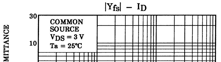
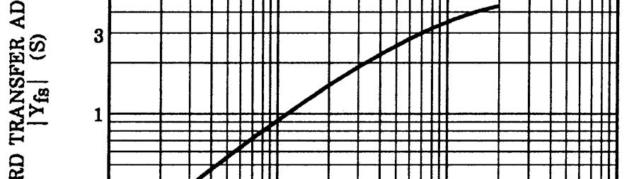
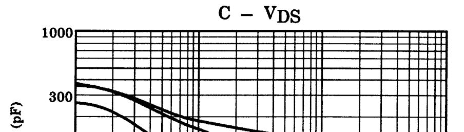
2 Electrical Characteristics (Ta = 25 C) Characteristics Symbol Test Condition Min Typ. Max Unit Gate leakage current I GSS V GS = ±10 V, V DS = 0 ±5 μa Drain-source breakdown voltage V (BR) DSS I D = 1 ma, V GS = 0 30 V Drain cut-off current I DSS V DS = 30 V, V GS = 0 1 μa Gate threshold voltage V th V DS = 3 V, I D = 0.1 ma V Forward transfer admittance Y fs V DS = 3 V, I D = 0.5 A (Note) 1.5 S Drain-source ON resistance R DS (ON) I D = 0.5 A, V GS = 4 V (Note) I D = 0.5 A, V GS = 2.5 V (Note) mω Input capacitance C iss V DS = 10 V, V GS = 0, f = 1 MHz 115 pf Reverse transfer capacitance C rss V DS = 10 V, V GS = 0, f = 1 MHz 24 pf Output capacitance C oss V DS = 10 V, V GS = 0, f = 1 MHz 60 pf Switching time Note: Pulse test Turn-off time t off V GS = 0~2.5 V, R G = 4.7 Ω 80 Turn-on time t on V DD = 15 V, I D = 0.5 A, 52 ns Switching Time Test Circuit Precaution V th can be expressed as voltage between gate and source when low operating current value is I D = 100 μa for this product. For normal switching operation, V GS (ON) requires higher voltage than V th and V GS (off) requires lower voltage than V th. (Relationship can be established as follows: V GS (off) < V th < V GS (ON) ) Please take this into consideration for using the device. 2
3 3


 4")
4 Figure mm 25.4 mm 1.6 t (a Cu pad of 0.8 mm 2 area) 4
5 RESTRICTIONS ON PRODUCT USE EN GENERAL The information contained herein is subject to change without notice. TOSHIBA is continually working to improve the quality and reliability of its products. Nevertheless, semiconductor devices in general can malfunction or fail due to their inherent electrical sensitivity and vulnerability to physical stress. It is the responsibility of the buyer, when utilizing TOSHIBA products, to comply with the standards of safety in making a safe design for the entire system, and to avoid situations in which a malfunction or failure of such TOSHIBA products could cause loss of human life, bodily injury or damage to property. In developing your designs, please ensure that TOSHIBA products are used within specified operating ranges as set forth in the most recent TOSHIBA products specifications. Also, please keep in mind the precautions and conditions set forth in the Handling Guide for Semiconductor Devices, or TOSHIBA Semiconductor Reliability Handbook etc. The TOSHIBA products listed in this document are intended for usage in general electronics applications (computer, personal equipment, office equipment, measuring equipment, industrial robotics, domestic appliances, etc.).these TOSHIBA products are neither intended nor warranted for usage in equipment that requires extraordinarily high quality and/or reliability or a malfunction or failure of which may cause loss of human life or bodily injury ( Unintended Usage ). Unintended Usage include atomic energy control instruments, airplane or spaceship instruments, transportation instruments, traffic signal instruments, combustion control instruments, medical instruments, all types of safety devices, etc.. Unintended Usage of TOSHIBA products listed in his document shall be made at the customer s own risk. The products described in this document shall not be used or embedded to any downstream products of which manufacture, use and/or sale are prohibited under any applicable laws and regulations. The information contained herein is presented only as a guide for the applications of our products. No responsibility is assumed by TOSHIBA for any infringements of patents or other rights of the third parties which may result from its use. No license is granted by implication or otherwise under any patents or other rights of TOSHIBA or the third parties. Please contact your sales representative for product-by-product details in this document regarding RoHS compatibility. Please use these products in this document in compliance with all applicable laws and regulations that regulate the inclusion or use of controlled substances. Toshiba assumes no liability for damage or losses occurring as a result of noncompliance with applicable laws and regulations. 5
TOSHIBA Field Effect Transistor Silicon P Channel MOS Type SSM3J16TE. DC I D 100 ma Pulse I DP 200
 High Speed Switching Applications Analog Switch Applications TOSHIBA Field Effect Transistor Silicon P Channel MOS Type SSMJ6TE Small package Low on-resistance : R on = 8 Ω (max) (@V GS = 4 V) : R on =
TOSHIBA Field-Effect Transistor Silicon P-Channel MOS Type SSM3J117TU. Characteristic Symbol Test Condition Min Typ. Max Unit
 TOSHIBA Field-Effect Transistor Silicon P-Channel MOS Type SSMJ7TU High-Speed Switching Applications 4 V drive Low ON-resistance: R on = 225 mω (max) (@V GS = ) R on = 7 mω (max) (@V GS = V) Absolute Maximum
TOSHIBA Field Effect Transistor Silicon N Channel MOS Type SSM3K17FU
 SSMK7FU TOSHIBA Field Effect Transistor Silicon N Channel MOS Type SSMK7FU High Speed Switching Applications Analog Switch Applications Unit: mm Suitable for high-density mounting due to compact package
TOSHIBA Field Effect Transistor Silicon N Channel MOS Type (π MOSV) 2SK3497
 2SK3497") TOSHIBA Field Effect Transistor Silicon N Channel MOS Type (π MOSV) High Power Amplifier Application Unit: mm High breakdown voltage: V DSS = 8 V Complementary to SJ68.. MAX. 5.9 MAX. Ф. ±... 9..5. ±..
TOSHIBA Field Effect Transistor Silicon N Channel MOS Type (π MOSV) High Power Amplifier Application Unit: mm High breakdown voltage: V DSS = 8 V Complementary to SJ68.. MAX. 5.9 MAX. Ф. ±... 9..5. ±..
TOSHIBA Field Effect Transistor Silicon P Channel MOS Type 2SJ168. DC I D 200 ma Pulse I DP 800
 TOSHIBA Field Effect Transistor Silicon P Channel MOS Type High Speed Switching Applications Analog Switch Applications Interface Applications Unit: mm Excellent switching time: ton = 14 ns (typ.) High
TOSHIBA Field Effect Transistor Silicon N Channel MOS Type (U-MOSIII) TPC6004
 TPC6004") TPC TOSHIBA Field Effect Transistor Silicon N Channel MOS Type (U-MOSIII) TPC Notebook PC Applications Portable Equipment Applications Unit: mm Low drain-source ON resistance: R DS (ON) = 9 mω (typ.) High
TPC TOSHIBA Field Effect Transistor Silicon N Channel MOS Type (U-MOSIII) TPC Notebook PC Applications Portable Equipment Applications Unit: mm Low drain-source ON resistance: R DS (ON) = 9 mω (typ.) High
TOSHIBA Field Effect Transistor Silicon N-Channel MOS Type (π-mos VI) 2SK4108. JEDEC Repetitive avalanche energy (Note 3) E AR 15 mj
 2SK4108. JEDEC Repetitive avalanche energy (Note 3) E AR 15 mj") SK TOSHIBA Field Effect Transistor Silicon N-Channel MOS Type (π-mos VI) SK Switching Regulator Applications Unit: mm Low drain source ON resistance : R DS (ON) =. Ω (typ.) High forward transfer admittance
SK TOSHIBA Field Effect Transistor Silicon N-Channel MOS Type (π-mos VI) SK Switching Regulator Applications Unit: mm Low drain source ON resistance : R DS (ON) =. Ω (typ.) High forward transfer admittance
TOSHIBA Field Effect Transistor Silicon N Channel MOS Type (π-mosvi) 2SK3667
 2SK3667") SK7 TOSHIBA Field Effect Transistor Silicon N Channel MOS Type (π-mosvi) SK7 Switching Regulator Applications Unit: mm Low drain-source ON resistance: R DS (ON) =.7Ω (typ.) High forward transfer admittance:
SK7 TOSHIBA Field Effect Transistor Silicon N Channel MOS Type (π-mosvi) SK7 Switching Regulator Applications Unit: mm Low drain-source ON resistance: R DS (ON) =.7Ω (typ.) High forward transfer admittance:
TOSHIBA Field Effect Transistor Silicon N-Channel MOS Type (Ultra-High-speed U-MOSIII) TPCA8011-H
 TPCA8011-H") TPCA-H TOSHIBA Field Effect Transistor Silicon N-Channel MOS Type (Ultra-High-speed U-MOSIII) TPCA-H High Efficiency DC/DC Converter Applications Notebook PC Applications Portable-Equipment Applications.±..7.±..
TPCA-H TOSHIBA Field Effect Transistor Silicon N-Channel MOS Type (Ultra-High-speed U-MOSIII) TPCA-H High Efficiency DC/DC Converter Applications Notebook PC Applications Portable-Equipment Applications.±..7.±..
TOSHIBA Field Effect Transistor Silicon N Channel MOS Type (DTMOS ) TK15J60U
 TK15J60U") TOSHIBA Field Effect Transistor Silicon N Channel MOS Type (DTMOS ) Switching Regulator Applications Unit: mm Low drain-source ON-resistance: R DS (ON) =. (typ.) High forward transfer admittance: Y fs
TOSHIBA Field Effect Transistor Silicon N Channel MOS Type (DTMOS ) Switching Regulator Applications Unit: mm Low drain-source ON-resistance: R DS (ON) =. (typ.) High forward transfer admittance: Y fs
TOSHIBA Field Effect Transistor Silicon N Channel MOS Type (U-MOS IV) TPC8026
 TPC8026") TPC26 TOSHIBA Field Effect Transistor Silicon N Channel MOS Type (U-MOS IV) TPC26 Lithium Ion Battery Applications Portable Equipment Applications Notebook PC Applications Unit: mm Small footprint due
TPC26 TOSHIBA Field Effect Transistor Silicon N Channel MOS Type (U-MOS IV) TPC26 Lithium Ion Battery Applications Portable Equipment Applications Notebook PC Applications Unit: mm Small footprint due
TOSHIBA Field Effect Transistor Silicon P Channel MOS Type (U-MOSⅣ) TPCA8103
 TPCA8103") TOSHIBA Field Effect Transistor Silicon P Channel MOS Type (U-MOSⅣ) TPCA83 TPCA83 Lithium Ion Battery Applications Notebook PC Applications Portable Equipment Applications.±..27 8.4±. Unit: mm. M A Small
TOSHIBA Field Effect Transistor Silicon P Channel MOS Type (U-MOSⅣ) TPCA83 TPCA83 Lithium Ion Battery Applications Notebook PC Applications Portable Equipment Applications.±..27 8.4±. Unit: mm. M A Small
TPCA8107-H 4± ± M A .0±.0± 0.15± ± ± ± ± ± 4.25±0.2 5±0. 3. Maximum Ratings (Ta 25 C)
") TOSHIBA Field Effect Transistor Silicon P-Channel MOS Type (Ultra-High-speed U-MOSIII) High Efficiency DC/DC Converter Applications Notebook PC Applications Portable Equipment Applications CCFL Inverter
TOSHIBA Field Effect Transistor Silicon P-Channel MOS Type (Ultra-High-speed U-MOSIII) High Efficiency DC/DC Converter Applications Notebook PC Applications Portable Equipment Applications CCFL Inverter
TOSHIBA Field Effect Transistor Silicon P-Channel MOS Type (U MOSIII) 2SJ668
 2SJ668") TOSHIBA Field Effect Transistor Silicon P-Channel MOS Type (U MOSIII) 2SJ668 Relay Drive, DC/DC Converter and Motor Drive Applications Unit: mm 4 V gate drive Low drain source ON-resistance: R DS (ON)
TOSHIBA Field Effect Transistor Silicon P-Channel MOS Type (U MOSIII) 2SJ668 Relay Drive, DC/DC Converter and Motor Drive Applications Unit: mm 4 V gate drive Low drain source ON-resistance: R DS (ON)
TOSHIBA Field Effect Transistor Silicon N-Channel MOS Type (U-MOSⅤ-H) TPC8037-H
 TPC8037-H") TOSHIBA Field Effect Transistor Silicon N-Channel MOS Type (U-MOSⅤ-H) TPC7-H TPC7-H High-Efficiency DC-DC Converter Applications Notebook PC Applications Portable Equipment Applications Unit: mm Small
TOSHIBA Field Effect Transistor Silicon N-Channel MOS Type (U-MOSⅤ-H) TPC7-H TPC7-H High-Efficiency DC-DC Converter Applications Notebook PC Applications Portable Equipment Applications Unit: mm Small
TOSHIBA Field Effect Transistor Silicon N Channel MOS Type (U-MOS IV) TPC8028
 TPC8028") TPC TOSHIBA Field Effect Transistor Silicon N Channel MOS Type (U-MOS IV) TPC Lithium Ion Battery Applications Portable Equipment Applications Notebook PC Applications Unit: mm Small footprint due to small
TPC TOSHIBA Field Effect Transistor Silicon N Channel MOS Type (U-MOS IV) TPC Lithium Ion Battery Applications Portable Equipment Applications Notebook PC Applications Unit: mm Small footprint due to small
TOSHIBA Field Effect Transistor Silicon N Channel MOS Type (π-mosⅦ) TK12A50D
 TK12A50D") TOSHIBA Field Effect Transistor Silicon N Channel MOS Type (π-mosⅦ) TKAD TKAD Switching Regulator Applications Unit: mm Low drain-source ON-resistance: R DS (ON) =. Ω (typ.) High forward transfer admittance:
TOSHIBA Field Effect Transistor Silicon N Channel MOS Type (π-mosⅦ) TKAD TKAD Switching Regulator Applications Unit: mm Low drain-source ON-resistance: R DS (ON) =. Ω (typ.) High forward transfer admittance:
TOSHIBA Field Effect Transistor Silicon N Channel MOS Type (DTMOS) TK40J60T
 TK40J60T") TKJT TOSHIBA Field Effect Transistor Silicon N Channel MOS Type (DTMOS) TKJT Switching Regulator Applications Unit: mm Low drain-source ON resistance: R DS (ON) =.Ω (typ.) High forward transfer admittance:
TKJT TOSHIBA Field Effect Transistor Silicon N Channel MOS Type (DTMOS) TKJT Switching Regulator Applications Unit: mm Low drain-source ON resistance: R DS (ON) =.Ω (typ.) High forward transfer admittance:
TOSHIBA Field Effect Transistor Silicon N Channel MOS Type (Ultra-High-Speed U-MOSIII) TPC8017-H
 TPC8017-H") TPC7-H TOSHIBA Field Effect Transistor Silicon N Channel MOS Type (Ultra-High-Speed U-MOSIII) TPC7-H High-Efficiency DC/DC Converter Applications Notebook PC Applications Portable-Equipment Applications
TPC7-H TOSHIBA Field Effect Transistor Silicon N Channel MOS Type (Ultra-High-Speed U-MOSIII) TPC7-H High-Efficiency DC/DC Converter Applications Notebook PC Applications Portable-Equipment Applications
TOSHIBA CMOS Digital Integrated Circuit Silicon Monolithic TC7SG02FU IN A GND
 TOSHIBA CMOS Digital Integrated Circuit Silicon Monolithic TC7SG02FU 2 Input NOR Gate Features High-level output current: I OH /I OL = ±8 ma (min) at = 3.0 High-speed operation: t pd = 2.4 ns (typ.) at
TOSHIBA Field Effect Transistor Silicon P Channel MOS Type (U-MOS III) TPCF8102
 TPCF8102") TOSHIBA Field Effect Transistor Silicon P Channel MOS Type (U-MOS III) TPCF82 TPCF82 Notebook PC Applications Portable Equipment Applications Unit: mm Low drain-source ON resistance: RDS (ON) = 24 mω (typ.)
TOSHIBA Field Effect Transistor Silicon P Channel MOS Type (U-MOS III) TPCF82 TPCF82 Notebook PC Applications Portable Equipment Applications Unit: mm Low drain-source ON resistance: RDS (ON) = 24 mω (typ.)
TOSHIBA Field Effect Transistor Silicon P Channel MOS Type (U-MOSⅣ) TPC8114. DC (Note 1) I D 18 A Pulse (Note 1) I DP 72
 TPC8114. DC (Note 1) I D 18 A Pulse (Note 1) I DP 72") TOSHIBA Field Effect Transistor Silicon P Channel MOS Type (U-MOSⅣ) TPC84 Lithium Ion Battery Applications Notebook PC Applications Portable Equipment Applications Unit: mm Small footprint due to small
TOSHIBA Field Effect Transistor Silicon P Channel MOS Type (U-MOSⅣ) TPC84 Lithium Ion Battery Applications Notebook PC Applications Portable Equipment Applications Unit: mm Small footprint due to small
TOSHIBA Field Effect Transistor Silicon N Channel MOS Type (L 2 π MOSV) 2SK2385
 2SK2385") TOSHIBA Field Effect Transistor Silicon N Channel MOS Type (L 2 π MOSV) 2SK2385 2SK2385 Chopper Regulator, DC DC Converter and Motor Drive Applications Unit: mm 4 V gate drive Low drain source ON resistance
TOSHIBA Field Effect Transistor Silicon N Channel MOS Type (L 2 π MOSV) 2SK2385 2SK2385 Chopper Regulator, DC DC Converter and Motor Drive Applications Unit: mm 4 V gate drive Low drain source ON resistance
TPCP8402 TPCP8402. Portable Equipment Applications Mortor Drive Applications DC-DC Converter Applications. Maximum Ratings (Ta = 25 C)
") TOSHIBA Field Effect Transistor Silicon P, N Channel MOS Type (U-MOS IV / U-MOS III) TPCP8402 Portable Equipment Applications Mortor Drive Applications DC-DC Converter Applications Unit: mm Low drain-source
TOSHIBA Field Effect Transistor Silicon P, N Channel MOS Type (U-MOS IV / U-MOS III) TPCP8402 Portable Equipment Applications Mortor Drive Applications DC-DC Converter Applications Unit: mm Low drain-source
TOSHIBA Field Effect Transistor Silicon N, P Channel MOS Type. (P Channel U MOS IV/N Channel U-MOS III) TPC8405. Rating P Channel N Channel
 TPC8405. Rating P Channel N Channel") TPC85 TOSHIBA Field Effect Transistor Silicon N, P Channel MOS Type Lithium Ion Secondary Battery Applications Portable Equipment Applications Notebook PC Applications (P Channel U MOS IV/N Channel U-MOS
TPC85 TOSHIBA Field Effect Transistor Silicon N, P Channel MOS Type Lithium Ion Secondary Battery Applications Portable Equipment Applications Notebook PC Applications (P Channel U MOS IV/N Channel U-MOS
TOSHIBA Field Effect Transistor Silicon N Channel MOS Type (π MOSV) 2SK2996
 2SK2996") TOSHIBA Field Effect Transistor Silicon N Channel MOS Type (π MOSV) 2SK2996 DC DC Converter, Relay Drive and Motor Drive Applications Unit: mm Low drain source ON resistance : RDS (ON) = 0.74 Ω (typ.)
TOSHIBA Field Effect Transistor Silicon N Channel MOS Type (π MOSV) 2SK2996 DC DC Converter, Relay Drive and Motor Drive Applications Unit: mm Low drain source ON resistance : RDS (ON) = 0.74 Ω (typ.)
TPC8203 TPC8203. Lithium Ion Battery Applications Portable Equipment Applications Notebook PCs. Maximum Ratings (Ta = 25 C) Circuit Configuration
 Circuit Configuration") TOSHIBA Field Effect Transistor Silicon N Channel MOS Type (U MOSII) TPC8203 Lithium Ion Battery Applications Portable Equipment Applications Notebook PCs Unit: mm Small footprint due to small and thin
TOSHIBA Field Effect Transistor Silicon N Channel MOS Type (U MOSII) TPC8203 Lithium Ion Battery Applications Portable Equipment Applications Notebook PCs Unit: mm Small footprint due to small and thin
TOSHIBA Field Effect Transistor Silicon N Channel MOS Type (π-mosvi) 2SK3567
 2SK3567") SK7 TOSHIBA Field Effect Transistor Silicon N Channel MOS Type (π-mosvi) SK7 Switching Regulator Applications Unit: mm Low drain-source ON resistance: RDS (ON) =.7Ω (typ.) High forward transfer admittance:
SK7 TOSHIBA Field Effect Transistor Silicon N Channel MOS Type (π-mosvi) SK7 Switching Regulator Applications Unit: mm Low drain-source ON resistance: RDS (ON) =.7Ω (typ.) High forward transfer admittance:
TOSHIBA Field Effect Transistor Silicon N Channel MOS Type (π-mosvi) 2SK3767
 2SK3767") SK77 TOSHIBA Field Effect Transistor Silicon N Channel MOS Type (π-mosvi) SK77 Switching Regulator Applications Unit: mm Low drain-source ON resistance: RDS (ON) =.Ω (typ.) High forward transfer admittance:
SK77 TOSHIBA Field Effect Transistor Silicon N Channel MOS Type (π-mosvi) SK77 Switching Regulator Applications Unit: mm Low drain-source ON resistance: RDS (ON) =.Ω (typ.) High forward transfer admittance:
TOSHIBA Field Effect Transistor Silicon N Channel MOS Type SSM6N15FE
 SSMNFE TOSHIBA Field Effect Transistor Silicon N Channel MOS Type SSMNFE High Speed Switching Applications Analog Switching Applications Unit: mm Small package Low ON resistance : R on =. Ω (max) (@V GS
TOSHIBA Field Effect Transistor Silicon N Channel MOS Type (π-mosⅣ) 2SK4013
 2SK4013") SK TOSHIBA Field Effect Transistor Silicon N Channel MOS Type (π-mosⅣ) SK Switching Regulator Applications Unit: mm Low drain-source ON resistance: RDS (ON) =. Ω (typ.) High forward transfer admittance:
SK TOSHIBA Field Effect Transistor Silicon N Channel MOS Type (π-mosⅣ) SK Switching Regulator Applications Unit: mm Low drain-source ON resistance: RDS (ON) =. Ω (typ.) High forward transfer admittance:
TOSHIBA Field Effect Transistor Silicon N Channel MOS Type (U MOSⅢ) TK30A06J3
 TK30A06J3") TOSHIBA Field Effect Transistor Silicon N Channel MOS Type (U MOSⅢ) Motor Drive Application Load Swithch Application Chopper Regulator and DC DC Converter Application Unit: mm Low drain-source ON resistance:
TOSHIBA Field Effect Transistor Silicon N Channel MOS Type (U MOSⅢ) Motor Drive Application Load Swithch Application Chopper Regulator and DC DC Converter Application Unit: mm Low drain-source ON resistance:
TOSHIBA Field Effect Transistor Silicon N Channel MOS Type (π-mosiv) 2SK3565
 2SK3565") SK TOSHIBA Field Effect Transistor Silicon N Channel MOS Type (π-mosiv) SK Switching Regulator Applications Unit: mm Low drain-source ON resistance: RDS (ON) =.Ω (typ.) High forward transfer admittance:
SK TOSHIBA Field Effect Transistor Silicon N Channel MOS Type (π-mosiv) SK Switching Regulator Applications Unit: mm Low drain-source ON resistance: RDS (ON) =.Ω (typ.) High forward transfer admittance:
TOSHIBA Field Effect Transistor Silicon N Channel MOS Type (π-mosv) 2SK3538
 2SK3538") SK TOSHIBA Field Effect Transistor Silicon N Channel MOS Type (π-mosv) SK Switching Regulator, DC-DC Converter Applications Unit: mm Low drain-source ON resistance: RDS (ON) = 7 mω (typ.) High forward
SK TOSHIBA Field Effect Transistor Silicon N Channel MOS Type (π-mosv) SK Switching Regulator, DC-DC Converter Applications Unit: mm Low drain-source ON resistance: RDS (ON) = 7 mω (typ.) High forward
TPCS8209 查询 TPCS8209 供应商 TPCS8209. Lithium Ion Battery Applications Notebook PC Applications Portable Machines and Tools. Maximum Ratings (Ta = 25 C)
") 查询 TPCS89 供应商 TPCS89 TOSHIBA Field Effect Transistor Silicon N Channel MOS Type (U-MOSIII) TPCS89 Lithium Ion Battery Applications Notebook PC Applications Portable Machines and Tools Unit: mm Small footprint
查询 TPCS89 供应商 TPCS89 TOSHIBA Field Effect Transistor Silicon N Channel MOS Type (U-MOSIII) TPCS89 Lithium Ion Battery Applications Notebook PC Applications Portable Machines and Tools Unit: mm Small footprint
TOSHIBA Field Effect Transistor Silicon N Channel MOS Type (U-MOSII) 2SK3236
 2SK3236") TOSHIBA Field Effect Transistor Silicon N Channel MOS Type (U-MOSII) 2SK3236 Switching Regulator Applications, DC-DC Converter and Motor Drive Applications Unit: mm V gate drive Low drain-source ON resistance:
TOSHIBA Field Effect Transistor Silicon N Channel MOS Type (U-MOSII) 2SK3236 Switching Regulator Applications, DC-DC Converter and Motor Drive Applications Unit: mm V gate drive Low drain-source ON resistance:
TPCF8402 F6B TPCF8402. Portable Equipment Applications Mortor Drive Applications DC-DC Converter Applications. Maximum Ratings (Ta = 25 C)
") TPCF84 TOSHIBA Field Effect Transistor Silicon P, N Channel MOS Type (U-MOS IV / U-MOS III) TPCF84 Portable Equipment Applications Mortor Drive Applications DC-DC Converter Applications Unit: mm Low drain-source
TPCF84 TOSHIBA Field Effect Transistor Silicon P, N Channel MOS Type (U-MOS IV / U-MOS III) TPCF84 Portable Equipment Applications Mortor Drive Applications DC-DC Converter Applications Unit: mm Low drain-source
TOSHIBA Field Effect Transistor Silicon N Channel MOS Type SSM6N44FE. DC I D 100 ma Pulse I DP 200
 SSMNFE TOSHIBA Field Effect Transistor Silicon N Channel MOS Type SSMNFE High Speed Switching Applications Analog Switching Applications.±. Unit: mm Compact package suitable for high-density mounting Low
TOSHIBA Field-Effect Transistor Silicon N Channel MOS Type (U-MOSⅣ) SSM6N7002BFU. DC I D 200 ma Pulse I DP 800
 SSM6N7002BFU. DC I D 200 ma Pulse I DP 800") TOSHIBA Field-Effect Transistor Silicon N Channel MOS Type (U-MOSⅣ) SSM6N7BFU High-Speed Switching Applications Analog Switch Applications Small package Low ON-resistance : R DS(ON) =. Ω (max) (@V GS =.
TOSHIBA Field-Effect Transistor Silicon N Channel MOS Type (U-MOSⅣ) SSM6N7BFU High-Speed Switching Applications Analog Switch Applications Small package Low ON-resistance : R DS(ON) =. Ω (max) (@V GS =.
TOSHIBA Field Effect Transistor Silicon N Channel MOS Type SSM6N37FU
 TOSHIBA Field Effect Transistor Silicon N Channel MOS Type SSM6N7FU High Speed Switching Applications Analog Switch Applications Unit: mm.v drive Low ON-resistance R DS(ON) =.6 Ω (max) (@V GS =. V) R DS(ON)
2SC3074 2SC3074. High Current Switching Applications. Maximum Ratings (Ta = 25 C)
") SC7 TOSHIBA Transistor Silicon NPN Epitaxial Type (PCT process) SC7 High Current Switching Applications Unit: mm Low collector saturation voltage: VCE (sat) =. V (max) (IC = A) High speed switching time:
SC7 TOSHIBA Transistor Silicon NPN Epitaxial Type (PCT process) SC7 High Current Switching Applications Unit: mm Low collector saturation voltage: VCE (sat) =. V (max) (IC = A) High speed switching time:
TOSHIBA Field-Effect Transistor Silicon N / P Channel MOS Type SSM6L35FE
 SSM6L3FE TOSHIBA Field-Effect Transistor Silicon N / P Channel MOS Type SSM6L3FE High-Speed Switching Applications Analog Switch Applications.6±. Unit: mm N-ch:.2-V drive.2±. P-ch:.2-V drive N-ch, P-ch,
GT10Q301 GT10Q301. High Power Switching Applications Motor Control Applications. Maximum Ratings (Ta = 25 C) Equivalent Circuit. Marking
 Equivalent Circuit. Marking") GTQ TOSHIBA Insulated Gate Bipolar Transistor Silicon N Channel IGBT GTQ High Power Switching Applications Motor Control Applications Unit: mm Third-generation IGBT Enhancement mode type High speed: tf
GTQ TOSHIBA Insulated Gate Bipolar Transistor Silicon N Channel IGBT GTQ High Power Switching Applications Motor Control Applications Unit: mm Third-generation IGBT Enhancement mode type High speed: tf
2SC4203 2SC4203. Video Output for High Definition VDT High Speed Switching Applications. Maximum Ratings (Ta = 25 C)
") TOSHIBA Transistor Silicon Epitaxial Planar Type 2SC42 Video Output for High Definition VDT High Speed Switching Applications Unit: mm High transition frequency: ft = 4 MHz (typ.) (VCE = V, IC = 7 ma)
TOSHIBA Transistor Silicon Epitaxial Planar Type 2SC42 Video Output for High Definition VDT High Speed Switching Applications Unit: mm High transition frequency: ft = 4 MHz (typ.) (VCE = V, IC = 7 ma)
TC4013BP,TC4013BF,TC4013BFN
 TOSHIBA CMOS Digital Integrated Circuit Silicon Monolithic TC4013BP,TC4013BF,TC4013BFN TC4013B Dual D-Type Flip Flop TC4013B contains two independent circuits of D type flip-flop. The input level applied
TC74LCX08F,TC74LCX08FN,TC74LCX08FT,TC74LCX08FK
 TOSHIBA CMOS Digital Integrated Circuit Silicon Monolithic TC74LCX08F/FN/FT/FK TC74LCX08F,TC74LCX08FN,TC74LCX08FT,TC74LCX08FK Low-Voltage Quad 2-Input AND Gate with 5-V Tolerant Inputs and Outputs The
MP6901 MP6901. High Power Switching Applications. Hammer Drive, Pulse Motor Drive and Inductive Load Switching. Maximum Ratings (Ta = 25 C)
") TOSHIBA Power Transistor Module Silicon Epitaxial Type (Darlington power transistor in ) High Power Switching Applications. Hammer Drive, Pulse Motor Drive and Inductive Load Switching. Industrial Applications
TOSHIBA Power Transistor Module Silicon Epitaxial Type (Darlington power transistor in ) High Power Switching Applications. Hammer Drive, Pulse Motor Drive and Inductive Load Switching. Industrial Applications
2SC5748 2SC5748. Horizontal Deflection Output for HDTV&Digital TV. Maximum Ratings (Tc 25 C) Electrical Characteristics (Tc 25 C)
 Electrical Characteristics (Tc 25 C)") TOSHIBA Transistor Silicon NPN Triple Diffused Mesa Type Horizontal Deflection Output for HDTV&Digital TV. Unit: mm High voltage: VCBO = V Low saturation voltage: VCE (sat) = V (max) High speed: tf =.
TOSHIBA Transistor Silicon NPN Triple Diffused Mesa Type Horizontal Deflection Output for HDTV&Digital TV. Unit: mm High voltage: VCBO = V Low saturation voltage: VCE (sat) = V (max) High speed: tf =.
TPCP8404 TPCP8404. Portable Equipment Applications Motor Drive Applications. Absolute Maximum Ratings (Ta = 25 C) Circuit Configuration
 Circuit Configuration") TOSHIBA Field Effect Transistor Silicon P, N Channel MOS Type (U-MOⅤ/U-MOSⅣ) TPCP8 Portable Equipment Applications Motor Drive Applications Low drain-source ON-resistance : P Channel R DS (ON) = 38 mω(typ.)
TOSHIBA Field Effect Transistor Silicon P, N Channel MOS Type (U-MOⅤ/U-MOSⅣ) TPCP8 Portable Equipment Applications Motor Drive Applications Low drain-source ON-resistance : P Channel R DS (ON) = 38 mω(typ.)
TC74LCX244F,TC74LCX244FW,TC74LCX244FT,TC74LCX244FK
 TOSHIBA CMOS Digital Integrated Circuit Silicon Monolithic TC74LCX244F/FW/FT/FK TC74LCX244F,TC74LCX244FW,TC74LCX244FT,TC74LCX244FK Low-Voltage Octal Bus Buffer with 5-V Tolerant Inputs and Outputs The
TC4066BP,TC4066BF,TC4066BFN,TC4066BFT
 TOSHIBA MOS Digital Integrated ircuit Silicon Monolithic T466BP/BF/BFN/BFT T466BP,T466BF,T466BFN,T466BFT T466B Quad Bilateral Switch T466B contains four independent circuits of bidirectional switches.
TC74VHCT573AF,TC74VHCT573AFW,TC74VHCT573AFT
 TOSHIBA CMOS igital Integrated Circuit Silicon Monolithic TC74HCT573AF/AFW/AFT TC74HCT573AF,TC74HCT573AFW,TC74HCT573AFT Octal -Type Latch with 3-State Output The TC74HCT573A is an advanced high speed CMOS
TA78033AS, TA7804AS, TA7805AS, TA7807AS, TA7808AS, TA7809AS
 TOSHIBA Bipolar Linear Integrated Circuit Silicon Monolithic TA7833AS, TA784AS, TA785AS, TA787AS, TA788AS, TA789AS TA7833, 4, 5, 7, 8, 9AS 1 A Three-Terminal Positive oltage Regulator The TA78***AS series
TOSHIBA Field Effect Transistor Silicon N Channel MOS Type (π MOSIII) 2SK2610
 2SK2610") TOSHIBA Field Effect Transistor Silicon N Channel MOS Type (π MOSIII) Chopper Regulator, DC DC Converter and Motor Drive Applications Unit: mm Low drain source ON resistance : RDS (ON) = 2.3 Ω (typ.) High
TOSHIBA Field Effect Transistor Silicon N Channel MOS Type (π MOSIII) Chopper Regulator, DC DC Converter and Motor Drive Applications Unit: mm Low drain source ON resistance : RDS (ON) = 2.3 Ω (typ.) High
TC74VHC164F,TC74VHC164FN,TC74VHC164FT,TC74VHC164FK
 TOSHIBA CMOS igital Integrated Circuit Silicon Monolithic TC74VHC164F/FN/FT/FK TC74VHC164F,TC74VHC164FN,TC74VHC164FT,TC74VHC164FK 8-Bit Shift egister (S-IN, P-OUT) The TC74VHC164 is an advanced high speed
TOSHIBA Field Effect Transistor Silicon P/N-Channel MOS Type (P-Channel/N-Channel Ultra-High-Speed U-MOSIII) TPC8406-H. Rating P-Channel N-Channel
 TPC8406-H. Rating P-Channel N-Channel") TPC86-H TOSHIBA Field Effect Transistor Silicon P/N-Channel MOS Type (P-Channel/N-Channel Ultra-High-Speed U-MOSIII) TPC86-H High Efficiency DC/DC Converter Applications Notebook PC Applications Portable
TPC86-H TOSHIBA Field Effect Transistor Silicon P/N-Channel MOS Type (P-Channel/N-Channel Ultra-High-Speed U-MOSIII) TPC86-H High Efficiency DC/DC Converter Applications Notebook PC Applications Portable
TOSHIBA Field Effect Transistor Silicon N Channel MOS Type (π-mosⅦ) TK6A50D
 TK6A50D") TOSHIBA Field Effect Transistor Silicon N Channel MOS Type (π-mosⅦ) TKAD TKAD Switching Regulator Applications Unit: mm Low drain-source ON-resistance: R DS (ON) =. Ω (typ.) High forward transfer admittance:
TOSHIBA Field Effect Transistor Silicon N Channel MOS Type (π-mosⅦ) TKAD TKAD Switching Regulator Applications Unit: mm Low drain-source ON-resistance: R DS (ON) =. Ω (typ.) High forward transfer admittance:
Rating Q1 Q (Note 4a)
") TPCA Q:TOSHIBA FIELD EFFECT TRANSISTOR SILICON N CHANNEL MOS TYPE(U-MOSⅢ) Q:TOSHIBA INCLUDES SCHOTTKY BARRIER DIODE FIELD EFFECT TRANSISTOR SILICON N CHANNEL MOS TYPE(U-MOSⅢ) TPCA DC-DC CONVERTER Notebook
TPCA Q:TOSHIBA FIELD EFFECT TRANSISTOR SILICON N CHANNEL MOS TYPE(U-MOSⅢ) Q:TOSHIBA INCLUDES SCHOTTKY BARRIER DIODE FIELD EFFECT TRANSISTOR SILICON N CHANNEL MOS TYPE(U-MOSⅢ) TPCA DC-DC CONVERTER Notebook
TA7262P,TA7262P(LB),TA7262F
,TA7262F") TOSHIBA BIPOLAR LINEAR INTEGRATED CIRCUIT SILICON MONOLITHIC TA7262P,TA7262P(LB),TA7262F DC MOTOR DRIVER (3 PHASE Bi DIRECTIONAL) The TA7262P / P (LB) / F are 3 Phase Bi Directional supply voltage control
TOSHIBA BIPOLAR LINEAR INTEGRATED CIRCUIT SILICON MONOLITHIC TA7262P,TA7262P(LB),TA7262F DC MOTOR DRIVER (3 PHASE Bi DIRECTIONAL) The TA7262P / P (LB) / F are 3 Phase Bi Directional supply voltage control
TOSHIBA Field Effect Transistor Silicon N Channel MOS Type (π-mosiii) 2SK2613
 2SK2613") SK6 TOSHIBA Field Effect Transistor Silicon N Channel MOS Type (π-mosiii) SK6 Switching Regulator Applications, DC-DC Converter and Motor Drive Applications Unit: mm Low drain-source ON-resistance: R DS
SK6 TOSHIBA Field Effect Transistor Silicon N Channel MOS Type (π-mosiii) SK6 Switching Regulator Applications, DC-DC Converter and Motor Drive Applications Unit: mm Low drain-source ON-resistance: R DS
TC74HC148AP,TC74HC148AF
 TOSHIBA CMOS Digital Integrated Circuit Silicon Monolithic TC74HC148AP,TC74HC148AF 8-to-3 Line Priority Encoder The TC74HC148A is a high speed CMOS 8-to-3 LINE ENCODER fabricated with silicon gate C2MOS
TC74HC74AP,TC74HC74AF,TC74HC74AFN
 TOSHIBA CMOS Digital Integrated Circuit Silicon Monolithic TC74HC74AP/AF/AFN TC74HC74AP,TC74HC74AF,TC74HC74AFN Dual D-Type Flip Flop Preset and Clear The TC74HC74A is a high speed CMOS D FLIP FLOP fabricated
TLP250 TLP250. Transistor Inverter Inverter For Air Conditioner IGBT Gate Drive Power MOS FET Gate Drive. Truth Table
 TOSHIB Photocoupler Gals Ired & Photo IC TLP20 Transistor Inverter Inverter For ir Conditioner IGBT Gate Drive Power MOS FET Gate Drive Unit in mm The TOSHIB TLP20 consists of a Gals light emitting diode
TC4511BP,TC4511BF TC4511BP/BF. TC4511B BCD-to-Seven Segment Latch/Decoder/Driver. Pin Assignment. Display
 TC411BP/BF TOSHIBA CMOS Digital Integrated Circuit Silicon Monolithic TC411BP,TC411BF TC411B BCD-to-Seven Segment Latch/Decoder/Driver TC411B is decoder which converts the input of BCD code into the 7
TC74HC373AP,TC74HC373AF,TC74HC373AFW
 TOSHIBA CMOS Digital Integrated Circuit Silicon Monolithic TC74HC373AP/AF/AFW TC74HC373AP,TC74HC373AF,TC74HC373AFW Octal D-Type Latch with 3-State Output The TC74HC373A is a high speed CMOS OCTAL LATCH
TC74HC7292AP,TC74HC7292AF
 TOSHIBA CMOS Digital Integrated Circuit Silicon Monolithic TC74HC7292AP,TC74HC7292AF Programmable Divider/Timer The TC74HC7292A is a high speed CMOS PROGRAMMABLE DIVIDER/TIMER fabricated with silicon gate
TC74HC4051AP,TC74HC4051AF,TC74HC4051AFT TC74HC4052AP,TC74HC4052AF,TC74HC4052AFT TC74HC4053AP,TC74HC4053AF,TC74HC4053AFN,TC74HC4053AFT
 T4H40,40P/F/FT,40P/F/FN/FT TOSHI MOS Digital Integrated ircuit Silicon Monolithic T4H40P,T4H40F,T4H40FT T4H40P,T4H40F,T4H40FT T4H40P,T4H40F,T4H40FN,T4H40FT T4H40P/F/FT 8-hannel nalog Multiplexer/Demulitiplexer
FG Silicon N-channel MOS FET (FET1) Silicon P-channel MOS FET (FET2) For switching circuits. Package. Overview. Features. Marking Symbol: V7
 Silicon P-channel MOS FET (FET2) For switching circuits. Package. Overview. Features. Marking Symbol: V7") FG6943 Silicon N-channel MOS FET (FET) Silicon P-channel MOS FET (FET2) For switching circuits Overview FG6943 is N-P channel dual type small signal MOS FET employed small size surface mounting package.
FG6943 Silicon N-channel MOS FET (FET) Silicon P-channel MOS FET (FET2) For switching circuits Overview FG6943 is N-P channel dual type small signal MOS FET employed small size surface mounting package.
TC4028BP, TC4028BF TC4028BP/BF. TC4028B BCD-to-Decimal Decoder. Pin Assignment TOSHIBA CMOS Digital Integrated Circuit Silicon Monolithic
 TOSHIBA CMOS Digital Integrated Circuit Silicon Monolithic TC4028BP, TC4028BF TC4028B BCD-to-Decimal Decoder TC4028B is a BCD-to-DECIMAL decoder which converts BCD signal into DECIMAL signal. Of ten outputs
TC74VHC574F,TC74VHC574FW,TC74VHC574FT,TC74VHC574FK
 TOSHIBA CMOS igital Integrated Circuit Silicon Monolithic TC74VHC574F/FW/FT/FK TC74VHC574F,TC74VHC574FW,TC74VHC574FT,TC74VHC574FK Octal -Type Flip Flop with 3-State Output The TC74VHC574 is advanced high
TC74VHC573F,TC74VHC573FW,TC74VHC573FT,TC74VHC573FK
 TOSHIBA CMOS igital Integrated Circuit Silicon Monolithic TC74VHC573F/FW/FT/FK TC74VHC573F,TC74VHC573FW,TC74VHC573FT,TC74VHC573FK Octal -Type Latch with 3-State Output The TC74VHC573 is an advanced high
TC74VCX14FT, TC74VCX14FK
 TOSHIBA CMOS Digital Integrated Circuit Silicon Monolithic TC74CX14FT, TC74CX14FK Low-oltage Hex Schmitt Inverter with 3.6- Tolerant Inputs and Outputs TC74CX14FT/FK The TC74CX14FT/FK is a high-performance
TC74HC155AP, TC74HC155AF
 TOSHIBA CMOS Digital Integrated Circuit Silicon Monolithic TC74HC155AP, TC74HC155AF Dual 2-to-4 Line Decoder 3-to-8 Line Decoder TC74HC155AP/AF The TC74HC155A is a high speed CMOS DUAL 2-to-4 LINE DECODER
IS2805 DESCRIPTION FEATURES
 DESCRIPTION The is an optically coupled isolator consists of two infrared emitting diodes in reverse parallel connection and optically coupled to an NPN silicon photo transistor. This device belongs to
TC7WB66CFK,TC7WB66CL8X TC7WB67CFK,TC7WB67CL8X
 CMOS Digital Integrated Circuits Silicon Monolithic TC7WB66CFK,TC7WB66CL8X TC7WB67CFK,TC7WB67CL8X 1. Functional Description Dual SPST Bus Switch 2. General TC7WB66CFK/L8X,TC7WB67CFK/L8X The TC7WB66CFK/L8X
PHD/PHP36N03LT. 1. Product profile. 2. Pinning information. N-channel TrenchMOS logic level FET. 1.1 General description. 1.
 Rev. 2 8 June 26 Product data sheet 1. Product profile 1.1 General description Logic level N-channel enhancement mode Field-Effect Transistor (FET) in a plastic package using TrenchMOS technology. 1.2
TPC8116-H TPC8116-H. High Efficiency DC/DC Converter Applications Notebook PC Applications Portable Equipment Applications CCFL Inverter Applications
 TOSHIBA Field Effect Transistor Silicon P-Channel MOS Type (Ultra-High-Speed U-MOSIII) High Efficiency DC/DC Converter Applications Notebook PC Applications Portable Equipment Applications CCFL Inverter
PSMN006-20K. N-channel TrenchMOS SiliconMAX ultra low level FET
 Rev. 7 November 29 Product data sheet. Product profile. General description SiliconMAX ultra low level N-channel enhancement mode Field-Effect Transistor (FET) in a plastic package using TrenchMOS technology.
60 V, 0.3 A N-channel Trench MOSFET
 Rev. 01 11 September 2009 Product data sheet 1. Product profile 1.1 General description ESD protected N-channel enhancement mode Field-Effect Transistor (FET) in a small SOT2 (TO-26AB) Surface-Mounted
PMWD16UN. 1. Product profile. 2. Pinning information. Dual N-channel µtrenchmos ultra low level FET. 1.1 General description. 1.
 Rev. 2 24 March 25 Product data sheet 1. Product profile 1.1 General description Dual N-channel enhancement mode Field-Effect Transistor (FET) in a plastic package using TrenchMOS technology. 1.2 Features
N-channel enhancement mode Field-Effect Transistor (FET) in a small SOT23 (TO-236AB) Surface-Mounted Device (SMD) plastic package using
 in a small SOT23 (TO-236AB) Surface-Mounted Device (SMD) plastic package using") Rev. 24 March 29 Product data sheet. Product profile. General description N-channel enhancement mode Field-Effect Transistor (FET) in a small SOT23 (TO-236AB) Surface-Mounted Device (SMD) plastic package
Rev. 24 March 29 Product data sheet. Product profile. General description N-channel enhancement mode Field-Effect Transistor (FET) in a small SOT23 (TO-236AB) Surface-Mounted Device (SMD) plastic package
BSS84 P-Channel Enhancement Mode Field-Effect Transistor
 BSS8 P-Channel Enhancement Mode Field-Effect Transistor Features -. A, - V, R DS(ON) = Ω at V GS = - V Voltage-Controlled P-Channel Small-Signal Switch High-Density Cell Design for Low R DS(ON) High Saturation
DATA SHEET. BSN304 N-channel enhancement mode vertical D-MOS transistor DISCRETE SEMICONDUCTORS. Product specification Supersedes data of 1997 Jun 17
 DISCRETE SEMICONDUCTORS DATA SHEET age M3D6 Supersedes data of 997 Jun 7 2 Dec FEATURES PINNING - TO-92 variant Direct interface to C-MOS, TTL, etc. High-speed switching No secondary breakdown. APPLICATIONS
PHT6N06T. 1. Product profile. 2. Pinning information. TrenchMOS standard level FET. 1.1 Description. 1.2 Features. 1.
 M3D87 Rev. 2 3 February 23 Product data 1. Product profile 1.1 Description N-channel enhancement mode field-effect transistor in a plastic package using TrenchMOS technology. Product availability: in SOT223.
P-channel enhancement mode MOS transistor
 FEATURES SYMBOL QUICK REFERENCE DATA Very low threshold voltage s V DS = 2 V Fast switching Logic level compatible I D =.2 A Subminiature surface mount g package R DS(ON). Ω (V GS =. V) GENERAL DESCRIPTION
2N7002T. 1. Product profile. 2. Pinning information. N-channel TrenchMOS FET. 1.1 General description. 1.2 Features. 1.
 Rev. 1 17 November 25 Product data sheet 1. Product profile 1.1 General description N-channel enhancement mode Field-Effect Transistor (FET) in a plastic package using TrenchMOS technology. 1.2 Features
PMV65XP. 1. Product profile. 2. Pinning information. P-channel TrenchMOS extremely low level FET. 1.1 General description. 1.
 Rev. 1 28 September 24 Product data sheet 1. Product profile 1.1 General description P-channel enhancement mode field effect transistor in a plastic package using TrenchMOS technology. 1.2 Features Low
N-channel TrenchMOS logic level FET
 Rev. 2 3 November 29 Product data sheet 1. Product profile 1.1 General description Logic level N-channel enhancement mode Field-Effect Transistor (FET) in a plastic package using TrenchMOS technology.
DATA SHEET. BSS192 P-channel enhancement mode vertical D-MOS transistor DISCRETE SEMICONDUCTORS. Product specification Supersedes data of 1997 Jun 20
 DISCRETE SEMICONDUCTORS DATA SHEET book, halfpage M3D19 Supersedes data of 1997 Jun 2 22 May 22 FEATURES Direct interface to C-MOS, TTL, etc. High-speed switching No secondary breakdown. APPLICATIONS Line
2N7002F. 1. Product profile. 2. Pinning information. N-channel TrenchMOS FET. 1.1 General description. 1.2 Features. 1.
 Rev. 3 28 April 26 Product data sheet. Product profile. General description N-channel enhancement mode Field-Effect Transistor (FET) in a plastic package using TrenchMOS technology..2 Features Logic level
PSMN004-60B. N-channel TrenchMOS SiliconMAX standard level FET. High frequency computer motherboard DC-to-DC convertors
 Rev. 2 15 December 29 Product data sheet 1. Product profile 1.1 General description SiliconMAX standard level N-channel enhancement mode Field-Effect Transistor (FET) in a plastic package using TrenchMOS
IS181 DESCRIPTION FEATURES
 DESCRIPTION The IS181 series of optocoupler consists of an infrared light emitting diode optically coupled to an NPN silicon photo transistor in a space efficient Mini Flat Package. FEATURES Low Profile
BUK9Y53-100B. N-channel TrenchMOS logic level FET. Table 1. Pinning Pin Description Simplified outline Symbol 1, 2, 3 source (S) 4 gate (G)
 4 gate (G)") Rev. 1 3 August 27 Product data sheet 1. Product profile 1.1 General description N-channel enhancement mode power Field-Effect Transistor (FET) in a plastic package using Nexperia High-Performance Automotive
Rev. 1 3 August 27 Product data sheet 1. Product profile 1.1 General description N-channel enhancement mode power Field-Effect Transistor (FET) in a plastic package using Nexperia High-Performance Automotive
PDM6UT20V08E N-Channel and P-Channel,20V,Small signal MOSFET
 N-Channel and P-Channel,2V,Small signal MOSFET Description The enhancement mode MOS is extremely high density cell and low on-resistance. D1 G2 S2 MOSFET Product Summary V DS (V) R DS(on) (Ω) I D (A).3@
N-channel TrenchMOS standard level FET. Higher operating power due to low thermal resistance Low conduction losses due to low on-state resistance
 Rev. 2 3 February 29 Product data sheet 1. Product profile 1.1 General description Standard level N-channel enhancement mode Field-Effect Transistor (FET) in a plastic package using TrenchMOS technology.
Derating of the MOSFET Safe Operating Area Outline:
 Outline: This document discusses temperature derating of the MOSFET safe operating area. Table of Contents Outline:... 1 Table of Contents... 2 1. Introduction... 3 2. What is the safe operating area?...
PSMN B. N-channel TrenchMOS SiliconMAX standard level FET. High frequency computer motherboard DC-to-DC convertors
 Rev. 2 6 July 29 Product data sheet 1. Product profile 1.1 General description SiliconMAX standard level N-channel enhancement mode Field-Effect Transistor (FET) in a plastic package using TrenchMOS technology.
DATA SHEET. BSN254; BSN254A N-channel enhancement mode vertical D-MOS transistor DISCRETE SEMICONDUCTORS
 DISCRETE SEMICONDUCTORS DATA SHEET book, halfpage M3D186 Supersedes data of 1997 Jun 23 22 Feb 19 FEATURES Direct interface to C-MOS, TTL, etc. High-speed switching No secondary breakdown Low R DSon. APPLICATIONS
Features. T A =25 o C unless otherwise noted
 NDS65 NDS65 P-Channel Enhancement Mode Field Effect Transistor General Description These P-Channel enhancement mode field effect transistors are produced using ON Semiconductor s proprietary, high cell
N-channel TrenchMOS standard level FET. High noise immunity due to high gate threshold voltage
 Rev. 2 12 March 29 Product data sheet 1. Product profile 1.1 General description Standard level N-channel enhancement mode Field-Effect Transistor (FET) in a plastic package using TrenchMOS technology.