Chapter 3. FET Amplifiers. Spring th Semester Mechatronics SZABIST, Karachi. Course Support
|
|
|
- Shanna Norton
- 6 years ago
- Views:
Transcription
1 Chapter 3 Spring th Semester Mechatronics SZABIST, Karachi 2 Course Support humera.rafique@szabist.edu.pk Office: 100 Campus (404) Official: ZABdesk ebooks: 1
2 Chapter Contents 3 J Small Signal Model Fixed Bias Configuration Self Bias Configuration Voltage Divider Configuration Common Gate Configuration Source Follower Configuration D and E type MOS Configurations Amplifier Network Design Cacade Configuration Applications 4 Small Signal Model 2
3 Small Signal Model 5 s Advantages: Excellent voltage gain High input impedance Low-power consumption Good frequency range Small Signal Model 6 Transconductance: The relationship of a change in I D to the corresponding change inv GS : g m I = V D GS 3
4 Small Signal Model 7 Mathematical Definition of g m : Where V GS =0V Where g m D G S D SS g m 1 VP g m 0 I = V 2I V = V 2I D S S = V g m = g m 0 1 g m = g m 0 1 P V V G S P V V G S P G S P Small Signal Model 8 Example 8-1: Determine the magnitude of g m for a J with I DSS = 8 ma and V P = 4 V at the following dc bias points: a. V GS = 0.5 V b. V GS = 1.5 V c. V GS = 2.5 V 4
5 Small Signal Model 9 Example 8-1: Determine the magnitude of g m for a J with I DSS = 8 ma and V P = 4 V at the following dc bias points: a. V GS = 0.5 V b. V GS = 1.5 V c. V GS = 2.5 V Small Signal Model 10 Example 8-2: For the J of Ex 8-1, find: a. g m (max) b. g m at each point of Ex 8-1 5
6 Small Signal Model 11 g m vs V GS : When V GS = V P, g m is zero When V GS = 0V, g m is maximum Small Signal Model 12 Example 8-3: Using J of Ex 8-1, plot g m vs V GS. 6
7 Small Signal Model 13 Example 8-3: Using J of Ex 8-1, plot g m vs V GS. g 2 I DSS m = V 1 P 2 I DSS g m 0 = V P V V GS P Small Signal Model 14 Effect of I D on g m : Shockley s equation: 1 V V GS P = I I D DSS V gm = gm0 1 V GS P g m = g m0 I I D DSS 7
8 Small Signal Model 15 Plot of of I D vs g m : g m = g m0 I I D DSS g = m 0 2 I V DSS P g m g mo I D I DSS g mo I DSS /2 0.5 g mo I DSS /4 0 0 ma Small Signal Model 16 Example 8-4: Plot g m vs I D of Ex 8-1: 8
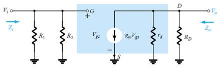
9 Example 8-4: Plot g m vs I D of Ex 8-1: Small Signal Model 17 G m I D g mo I DSS g mo I DSS /2 0.5 g mo I DSS /4 0 0 ma Small Signal Model 18 J Z i : input impedance, Z i is sufficiently large. Usually in the range of 10 9 Ω (1000MΩ) Zi ( ) = Ω J Z o : output impedance, Zo is similar in magnitude to conventional BJTs. Output impedance appears as y os with units of µs where 1 Z o = rd = yos VDS r d = VGS = constant ID 9
10 Small Signal Model 19 Defining r d using J characteristics: Small Signal Model 20 Example 8.5: Determine the output impedance for the given J for V GS = 0 V and 2V at V DS = 8V. 10


11 Small Signal Model 21 J AC Equivalent: Small Signal Model 22 Example 8-6: Given y fs = 3.8 ms and y os = 20 µs. Sketch the ac equivalent model: Ω 11
 Important Parameters of AC Analysis: 1. Input impedance 2. Output impedance 3.")
12 23 J Configurations J Configurations 24 J Configurations: 1. Fixed bias (Common Source) 2. Self bias 3. Voltage-Divider bias 4. Common Gate 5. Source-Follower (Common Drain) Important Parameters of AC Analysis: 1. Input impedance 2. Output impedance 3. Voltage Gain 12
13 25 Fixed Bias Configuration J Fixed Bias Fixed Bias Configuration (Common Source): 13

 Z = R i G")
14 J Fixed Bias 27 Determining Z i : Substituting the J ac equivalent circuit unit into the fixed bias network J Fixed Bias 28 Determining Z i : ( ) Z = R i G Redrawn network 14
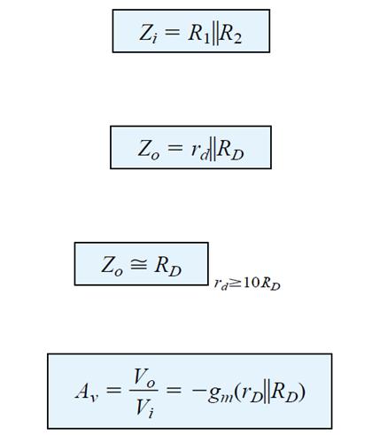
 ( ) v o i = -g r R A = V v o i = -g R when r 10R m D d D V = -g V V ( r R ) o m gs d D gs = V i ( ) V = -g V r R o m i d D Phase reversal")
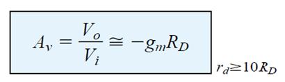
15 J Fixed Bias 29 Determining Z o : Set Vi = 0 Z Z o ( ) = r R o d D ( ) if r = R d 10R D D J Fixed Bias 30 Determining A V : A = V ( V ) m ( d D ) ( V ) ( ) v o i = -g r R A = V v o i = -g R when r 10R m D d D V = -g V V ( r R ) o m gs d D gs = V i ( ) V = -g V r R o m i d D Phase reversal 15
16 J Fixed Bias 31 Example 8-7: AC analysis of the fixed-bias configuration of Ex 7-1: If y os = 40 µs, than, determine: a. g m b. r d c. Z i d. Z o e. A v f. A v (ignoring the effects of r d ) I DQ =5.625mA; V GSQ = 2V y OS =40µS 32 Self Bias Configuration 16

17 J Self Bias 33 J Self Bias: Bypassed R S J Self Bias 34 J Self Bias: Fixed bias network following the substitution of the J ac equivalent 17

18 J Self Bias 35 J Self Bias: Redrawn network J Self Bias 36 J Self Bias: Unbypassed R S Z i = R Z G V o o = = I o R D 18

19 J Self Bias 37 J Self Bias: Unbypassed R S Including the effects of r d in the self bias J configuration J Self Bias 38 J Self Bias: Unbypassed R S R S 1 + g m RS + r d Z O = R RS R D 1 + g m RS + + rd rd D Z O R D A v V O g m R D g m R D = = V RS + R D 1+ g 1 g R m R + S + r i m S d 19
20 J Self Bias 39 Example 8-8: AC Analysis the self-bias configuration of Ex 7-2: If y os = 20 µs, then, determine: a. g m b. r d c. Z i d. Z o (with and without the effects of r d ). Compare the results. e. A v (with and without the effects of r d ). Compare the results. J Self Bias 40 Computer Analysis: 20
21 41 Voltage Divider Configuration J Voltage Divider Bias 42 Voltage Divider Bias: 21

22 J Voltage Divider Bias 43 Voltage Divider Bias: J Voltage Divider Bias 44 Voltage Divider Bias: Z = R R i 1 2 Z o R D A V = g R o v m D V i 22

23 45 Common-Gate Configuration J Common-Gate 46 Common Gate Configuration: 23

24 J Common-Gate 47 Common Gate Configuration: J Common-Gate 48 Common Gate Configuration: Z ' i R D 1 + r d 1 g m + rd Z i R Z S o 1 g R m D A R g v D m 24
25 J Common-Gate 49 Example 8-9: Determine: a. g m b. r d c. Z i d. Z o (with and without the effects of r d ). Compare the results. a. V o (with and without the effects of r d ). Compare the results. 50 Source-Follower (Common-Drain) Configuration 25
 52 Source-Follower (CD):")
26 J Source-Follower (CD) 51 Source-Follower (CD): J Source-Follower (CD) 52 Source-Follower (CD): 26
 54 Common-Follower (CD):")
27 J Source-Follower (CD) 53 Common-Follower (CD): J Source-Follower (CD) 54 Common-Follower (CD): Determining Z o 27
28 J Source-Follower (CD) 55 Common-Follower (CD): Z i = R G Z o R S 1 g m Av g m RS 1 + g R m S J Source-Follower (CD) 56 Example 8-10: AC analysis: V GSQ = 2.86 V and I DQ = 4.56 ma. Determine: a. g m b. R d c. Z i d. Z o with and without r d. Compare results. e. A v with and without r d. Compare results. 28
29 57 Depletion-Type MOSs MOS Configurations 58 MOS Configurations: D-MOS: 1. Voltage Divider E-MOS: 1. Drain Feedback 2. Voltage Divider 29

30 59 D-MOS D-MOS Configurations 60 D-MOS Equivalent Model: 30

31 D-MOS Configurations 61 Example 8-11: AC analysis (Ex 7-8): V GSQ = 0.36 V and I DQ = 7.6 ma. Determine: a. g m and compare to g mo. b. r d c. Z i d. Z o e. A v f. Sketch the ac equivalent D-MOS Configurations 62 Example 8-11: 31

32 63 E-MOS E-MOS Configurations 64 Equivalent Circuit: 32
33 65 E-MOS Drain-Feedback E-MOS Configurations 66 Drain Feedback: 33

34 E-MOS Configurations 67 Drain Feedback: E-MOS Configurations 68 Drain Feedback: Determining Z o 34

 Calculate Z i with and without r d. Compare results. c) Find Z o with and without r d. Compare results. d) Find A v with and without r d.")
35 E-MOS Configurations 69 Drain Feedback: A v = g m (R F r d R D ) A v = g m R D E-MOS Configurations 70 Example 8-12: The E-MOS of Fig was analyzed in Example 7.11, with the result that k = 0.24 x 10 3 A/V 2, V GSQ = 6.4 V, and I DQ = 2.75 ma. Determine gm. a) Find r d. b) Calculate Z i with and without r d. Compare results. c) Find Z o with and without r d. Compare results. d) Find A v with and without r d. Compare results. 35
36 71 E-MOS Voltage Divider E-MOS Configurations 72 Voltage Divider: 36
37 E-MOS Configurations 73 Voltage Divider: E-MOS Configurations 74 Voltage Divider: 37
38 75 Designing Amplifier Network Amplifier Network Designing 76 Example 8-13: Design the fixed-bias network of Fig to have an ac gain of 10. That is determine the value of R D. 38
39 Amplifier Network Designing 77 Example 8-14: With a relatively high level of g m, select the values of R D and R S for the given network, that will result in a gain of 8. For the device V GSQ = ¼ V P. Amplifier Network Designing 78 Example 8-15: With a relatively high level of g m, select the values of R D and R S for the given network, that will result in a gain of 8. For the device V GSQ = ¼ V P. Now bypass capacitor has been removed. 39

40 Summary Table 79 Summary Table 80 40
41 Summary Table 81 Summary Table 82 41

42 83 Effect of R L and R sig R L and R sig 84 Effect of R L and R sig :. 42


43 R L and R sig 85 Effect of R L and R sig : R L and R sig 86 Effect of R L and R sig :. 43
44 87 Cascade Configuration Cascade Configuration 88 Cascade Configuration: V i1 A v1 V O1 =V i2 A v2 V O2 A = A... 1A 2 v v v 44
45 Cascade Configuration 89 Cascade Configuration: Cascade Configuration 90 Example 8-16: Calculate the dc bias, voltage gain, input impedance, output impedance and resulting output voltage for the cascade amplifier shown in Fig Calculate the load voltage if a 10-k load is connected across the output. 45
46 Cascade Configuration 91 Example 8-17: For the cascade amplifier of Fig. 8-50, use the dc bias calculated in Example 8-15 and 8-16 to calculate the input impedance, output impedance, voltage gain, and resulting output voltage. 92 Practical Applications 46
47 Practical Applications Three channel audio mixer Practical Applications Phase Shift network 47
48 Home Task 95 Reading: 1. Summary 2. Equations 3. Computer analysis Problems: 1. Sec 8.2: (odd) 2. Sec 8.3: 17,18 3. Sec 8.4: 19,21 4. Sec 8.5:23,25 5. Sec 8.6: 27,29 6. Sec 8.7: Sec 8.8: 33,35,37 8. Sec 8.10: 39,41 9. Sec 8.11: Sec 8.12: Sec 8.14: Sec 8.15: 49 Refernces Bolestad 2. Paynter CH 13 48
Chapter7. FET Biasing
 Chapter7. J configurations Fixed biasing Self biasing & Common Gate Voltage divider MOS configurations Depletion-type Enhancement-type JFET: Fixed Biasing Example 7.1: As shown in the figure, it is the
CHAPTER 3: TRANSISTOR MOSFET DR. PHAM NGUYEN THANH LOAN. Hà Nội, 9/24/2012
 1 CHAPTER 3: TRANSISTOR MOSFET DR. PHAM NGUYEN THANH LOAN Hà Nội, 9/24/2012 Chapter 3: MOSFET 2 Introduction Classifications JFET D-FET (Depletion MOS) MOSFET (Enhancement E-FET) DC biasing Small signal
FET Small-Signal Analysis
 CHAPTER FET mall-ignal Analysis 9 9.1 INTROUCTION Field-effect transistor amplifiers provide an excellent voltage gain with the added feature of a high input impedance. They are also considered low-power
JFET Operating Characteristics: V GS = 0 V 14. JFET Operating Characteristics: V GS = 0 V 15
 J Operating Characteristics: V GS = 0 V 14 V GS = 0 and V DS increases from 0 to a more positive voltage: Gate and Source terminals: at the same potential Drain: at positive potential => reverse biased
Chapter 6: Field-Effect Transistors
 Chapter 6: Field-Effect Transistors slamic University of Gaza Dr. Talal Skaik FETs vs. BJTs Similarities: Amplifiers Switching devices mpedance matching circuits Differences: FETs are voltage controlled
EE105 Fall 2014 Microelectronic Devices and Circuits
 EE05 Fall 204 Microelectronic Devices and Circuits Prof. Ming C. Wu wu@eecs.berkeley.edu 5 Sutardja Dai Hall (SDH) Terminal Gain and I/O Resistances of BJT Amplifiers Emitter (CE) Collector (CC) Base (CB)
ECE 523/421 - Analog Electronics University of New Mexico Solutions Homework 3
 ECE 523/42 - Analog Electronics University of New Mexico Solutions Homework 3 Problem 7.90 Show that when ro is taken into account, the voltage gain of the source follower becomes G v v o v sig R L r o
6.012 Electronic Devices and Circuits Spring 2005
 6.012 Electronic Devices and Circuits Spring 2005 May 16, 2005 Final Exam (200 points) -OPEN BOOK- Problem NAME RECITATION TIME 1 2 3 4 5 Total General guidelines (please read carefully before starting):
Lecture 11: J-FET and MOSFET
 ENE 311 Lecture 11: J-FET and MOSFET FETs vs. BJTs Similarities: Amplifiers Switching devices Impedance matching circuits Differences: FETs are voltage controlled devices. BJTs are current controlled devices.
CLASS 12&13 JFET PARAMETERS AND BIASING
 CLASS 12&13 JFET PARAMETERS AN BIASING The family of drain characteristic curves shows that when GS becomes more negative, Sp (or S(sat) )andi S become smaller. I is dependent on the width of the channel.
Homework Assignment 09
 Homework Assignment 09 Question 1 (Short Takes) Two points each unless otherwise indicated. 1. What is the 3-dB bandwidth of the amplifier shown below if r π = 2.5K, r o = 100K, g m = 40 ms, and C L =
Chapter 5. BJT AC Analysis
 Chapter 5. Outline: The r e transistor model CB, CE & CC AC analysis through r e model common-emitter fixed-bias voltage-divider bias emitter-bias & emitter-follower common-base configuration Transistor
Chapter 13 Small-Signal Modeling and Linear Amplification
 Chapter 13 Small-Signal Modeling and Linear Amplification Microelectronic Circuit Design Richard C. Jaeger Travis N. Blalock 1/4/12 Chap 13-1 Chapter Goals Understanding of concepts related to: Transistors
ECE 546 Lecture 11 MOS Amplifiers
 ECE 546 Lecture MOS Amplifiers Spring 208 Jose E. Schutt-Aine Electrical & Computer Engineering University of Illinois jesa@illinois.edu ECE 546 Jose Schutt Aine Amplifiers Definitions Used to increase
EE 330. Lecture 35. Parasitic Capacitances in MOS Devices
 EE 330 Lecture 35 Parasitic Capacitances in MOS Devices Exam 2 Wed Oct 24 Exam 3 Friday Nov 16 Review from Last Lecture Cascode Configuration Discuss V CC gm1 gm1 I B VCC V OUT g02 g01 A - β β VXX Q 2
Circle the one best answer for each question. Five points per question.
 ID # NAME EE-255 EXAM 3 November 8, 2001 Instructor (circle one) Talavage Gray This exam consists of 16 multiple choice questions and one workout problem. Record all answers to the multiple choice questions
SD2902. RF POWER TRANSISTORS HF/VHF/UHF N-CHANNEL MOSFETs
 SD292 RF POWER TRANSISTORS HF/VHF/UHF N-CHANNEL MOSFETs GOLD METALLIZATION COMMON SOURCE CONFIGURATION 2 - MHz WATTS 28 VOLTS 12. db MIN. AT 4 MHz CLASS A OR AB OPERATION EXCELLENT THERMAL STABILITY DESCRIPTION
ECE-342 Test 3: Nov 30, :00-8:00, Closed Book. Name : Solution
 ECE-342 Test 3: Nov 30, 2010 6:00-8:00, Closed Book Name : Solution All solutions must provide units as appropriate. Unless otherwise stated, assume T = 300 K. 1. (25 pts) Consider the amplifier shown
Vidyalankar S.E. Sem. III [EXTC] Analog Electronics - I Prelim Question Paper Solution
![Vidyalankar S.E. Sem. III [EXTC] Analog Electronics - I Prelim Question Paper Solution](/thumbs/90/101612294.jpg "Vidyalankar S.E. Sem. III [EXTC] Analog Electronics - I Prelim Question Paper Solution") . (a) S.E. Sem. [EXTC] Analog Electronics - Prelim Question Paper Solution Comparison between BJT and JFET BJT JFET ) BJT is a bipolar device, both majority JFET is an unipolar device, electron and minority
. (a) S.E. Sem. [EXTC] Analog Electronics - Prelim Question Paper Solution Comparison between BJT and JFET BJT JFET ) BJT is a bipolar device, both majority JFET is an unipolar device, electron and minority
Lecture 13 MOSFET as an amplifier with an introduction to MOSFET small-signal model and small-signal schematics. Lena Peterson
 Lecture 13 MOSFET as an amplifier with an introduction to MOSFET small-signal model and small-signal schematics Lena Peterson 2015-10-13 Outline (1) Why is the CMOS inverter gain not infinite? Large-signal
CHAPTER.4: Transistor at low frequencies
 CHAPTER.4: Transistor at low frequencies Introduction Amplification in the AC domain BJT transistor modeling The re Transistor Model The Hybrid equivalent Model Introduction There are three models commonly
Chapter 4 Field-Effect Transistors
 Chapter 4 Field-Effect Transistors Microelectronic Circuit Design Richard C. Jaeger Travis N. Blalock 5/5/11 Chap 4-1 Chapter Goals Describe operation of MOSFETs. Define FET characteristics in operation
(Refer Slide Time: 1:49)
") Analog Electronic Circuits Professor S. C. Dutta Roy Department of Electrical Engineering Indian Institute of Technology Delhi Lecture no 14 Module no 01 Midband analysis of FET Amplifiers (Refer Slide
Analog Electronic Circuits Professor S. C. Dutta Roy Department of Electrical Engineering Indian Institute of Technology Delhi Lecture no 14 Module no 01 Midband analysis of FET Amplifiers (Refer Slide
Lecture 10 MOSFET (III) MOSFET Equivalent Circuit Models
 MOSFET Equivalent Circuit Models") Lecture 10 MOSFET (III) MOSFET Equivalent Circuit Models Outline Lowfrequency smallsignal equivalent circuit model Highfrequency smallsignal equivalent circuit model Reading Assignment: Howe and Sodini;
Lecture 10 MOSFET (III) MOSFET Equivalent Circuit Models Outline Lowfrequency smallsignal equivalent circuit model Highfrequency smallsignal equivalent circuit model Reading Assignment: Howe and Sodini;
TPC8116-H TPC8116-H. High Efficiency DC/DC Converter Applications Notebook PC Applications Portable Equipment Applications CCFL Inverter Applications
 TOSHIBA Field Effect Transistor Silicon P-Channel MOS Type (Ultra-High-Speed U-MOSIII) High Efficiency DC/DC Converter Applications Notebook PC Applications Portable Equipment Applications CCFL Inverter
Investigation of the Thermal Noise of MOS Transistors under Analog and RF Operating Conditions
 Investigation of the Thermal Noise of MOS Transistors under Analog and RF Operating Conditions Ralf Brederlow 1, Georg Wenig 2, and Roland Thewes 1 1 Infineon Technologies, Corporate Research, 2 Technical
UNIVERSITY OF CALIFORNIA College of Engineering Department of Electrical Engineering and Computer Sciences
 UNIVERSITY OF CALIFORNIA College of Engineering Department of Electrical Engineering and Computer Sciences E. Alon Final EECS 240 Monday, May 19, 2008 SPRING 2008 You should write your results on the exam
Delhi Noida Bhopal Hyderabad Jaipur Lucknow Indore Pune Bhubaneswar Kolkata Patna Web: Ph:
 Serial : ND_EE_NW_Analog Electronics_05088 Delhi Noida Bhopal Hyderabad Jaipur Lucknow ndore Pune Bhubaneswar Kolkata Patna Web: E-mail: info@madeeasy.in Ph: 0-4546 CLASS TEST 08-9 ELECTCAL ENGNEENG Subject
Homework Assignment 08
 Homework Assignment 08 Question 1 (Short Takes) Two points each unless otherwise indicated. 1. Give one phrase/sentence that describes the primary advantage of an active load. Answer: Large effective resistance
Lecture 15: MOS Transistor models: Body effects, SPICE models. Context. In the last lecture, we discussed the modes of operation of a MOS FET:
 Lecture 15: MOS Transistor models: Body effects, SPICE models Context In the last lecture, we discussed the modes of operation of a MOS FET: oltage controlled resistor model I- curve (Square-Law Model)
Microelectronic Circuit Design 4th Edition Errata - Updated 4/4/14
 Chapter Text # Inside back cover: Triode region equation should not be squared! i D = K n v GS "V TN " v & DS % ( v DS $ 2 ' Page 49, first exercise, second answer: -1.35 x 10 6 cm/s Page 58, last exercise,
Maximum Ratings, at T j = 25 C, unless otherwise specified Parameter Symbol Value Unit Continuous drain current I D. I D puls 0.68.
 SIPMOS Small-Signal-Transistor Feature N-Channel Enhancement mode Logic Level dv/dt rated Gate pin1 Product Summary V DS 1 V R DS(on) 6 Ω I D.17 Drain pin 3 Source pin 2 PG-SOT23 3 1 2 VPS5161 Type Package
Lecture 18. Common Source Stage
 ecture 8 OUTINE Basic MOSFET amplifier MOSFET biasing MOSFET current sources Common source amplifier eading: Chap. 7. 7.7. EE05 Spring 008 ecture 8, Slide Prof. Wu, UC Berkeley Common Source Stage λ =
AOP606 Complementary Enhancement Mode Field Effect Transistor
 AOP66 Complementary Enhancement Mode Field Effect Transistor General Description The AOP66 uses advanced trench technology MOSFETs to provide excellent and low gate charge. The complementary MOSFETs may
Lecture 24 Multistage Amplifiers (I) MULTISTAGE AMPLIFIER
 MULTISTAGE AMPLIFIER") Lecture 24 Multistage Amplifiers (I) MULTISTAGE AMPLIFIER Outline. Introduction 2. CMOS multi-stage voltage amplifier 3. BiCMOS multistage voltage amplifier 4. BiCMOS current buffer 5. Coupling amplifier
Lecture 24 Multistage Amplifiers (I) MULTISTAGE AMPLIFIER Outline. Introduction 2. CMOS multi-stage voltage amplifier 3. BiCMOS multistage voltage amplifier 4. BiCMOS current buffer 5. Coupling amplifier
Chapter 9 Frequency Response. PART C: High Frequency Response
 Chapter 9 Frequency Response PART C: High Frequency Response Discrete Common Source (CS) Amplifier Goal: find high cut-off frequency, f H 2 f H is dependent on internal capacitances V o Load Resistance
ID # NAME. EE-255 EXAM 3 April 7, Instructor (circle one) Ogborn Lundstrom
 Ogborn Lundstrom") ID # NAME EE-255 EXAM 3 April 7, 1998 Instructor (circle one) Ogborn Lundstrom This exam consists of 20 multiple choice questions. Record all answers on this page, but you must turn in the entire exam.
ID # NAME EE-255 EXAM 3 April 7, 1998 Instructor (circle one) Ogborn Lundstrom This exam consists of 20 multiple choice questions. Record all answers on this page, but you must turn in the entire exam.
Preliminary data. Maximum Ratings,at T j = 25 C, unless otherwise specified Parameter Symbol Value Unit Continuous drain current I D.
 OptiMOS -P Small-Signal-Transistor Feature P-Channel Enhancement mode Super Logic Level (. V rated) C operating temperature valanche rated dv/dt rated Product Summary V DS - V R DS(on) 7 mω I D -. SOT-
AO4620 Complementary Enhancement Mode Field Effect Transistor
 AO46 Complementary Enhancement Mode Field Effect Transistor General Description The AO46 uses advanced trench technology MOSFETs to provide excellent and low gate charge. The complementary MOSFETs may
DISCRETE SEMICONDUCTORS DATA SHEET. BLF246 VHF power MOS transistor Oct 21. Product specification Supersedes data of September 1992
 DISCRETE SEMICONDUCTORS DATA SHEET Supersedes data of September 1992 1996 Oct 21 FEATURES High power gain Low noise figure Easy power control Good thermal stability Withstands full load mismatch. PINNING
Advanced Current Mirrors and Opamps
 Advanced Current Mirrors and Opamps David Johns and Ken Martin (johns@eecg.toronto.edu) (martin@eecg.toronto.edu) slide 1 of 26 Wide-Swing Current Mirrors I bias I V I in out out = I in V W L bias ------------
TOSHIBA Field-Effect Transistor Silicon P-Channel MOS Type SSM3J117TU. Characteristic Symbol Test Condition Min Typ. Max Unit
 TOSHIBA Field-Effect Transistor Silicon P-Channel MOS Type SSMJ7TU High-Speed Switching Applications 4 V drive Low ON-resistance: R on = 225 mω (max) (@V GS = ) R on = 7 mω (max) (@V GS = V) Absolute Maximum
BSS123. Rev K/W. R thja
 Thermal Characteristics Parameter Symbol Values Unit min. typ. max. Characteristics Thermal resistance, junction - ambient at minimum footprint R thj - - 35 K/W Electrical Characteristics, at T j = 25
TOSHIBA Field Effect Transistor Silicon N Channel MOS Type (π-mosⅦ) TK6A50D
 TK6A50D") TOSHIBA Field Effect Transistor Silicon N Channel MOS Type (π-mosⅦ) TKAD TKAD Switching Regulator Applications Unit: mm Low drain-source ON-resistance: R DS (ON) =. Ω (typ.) High forward transfer admittance:
TOSHIBA Field Effect Transistor Silicon N Channel MOS Type (π-mosⅦ) TKAD TKAD Switching Regulator Applications Unit: mm Low drain-source ON-resistance: R DS (ON) =. Ω (typ.) High forward transfer admittance:
Monolithic N-Channel JFET Dual
 N9 Monolithic N-Channel JFET Dual V GS(off) (V) V (BR)GSS Min (V) g fs Min (ms) I G Max (pa) V GS V GS Max (mv). to. Monolithic Design High Slew Rate Low Offset/Drift Voltage Low Gate Leakage: pa Low Noise:
TOSHIBA Field Effect Transistor Silicon N Channel MOS Type (π MOSIII) 2SK2610
 2SK2610") TOSHIBA Field Effect Transistor Silicon N Channel MOS Type (π MOSIII) Chopper Regulator, DC DC Converter and Motor Drive Applications Unit: mm Low drain source ON resistance : RDS (ON) = 2.3 Ω (typ.) High
TOSHIBA Field Effect Transistor Silicon N Channel MOS Type (π MOSIII) Chopper Regulator, DC DC Converter and Motor Drive Applications Unit: mm Low drain source ON resistance : RDS (ON) = 2.3 Ω (typ.) High
DISCRETE SEMICONDUCTORS DATA SHEET. BLF245 VHF power MOS transistor
 DISCRETE SEMICONDUCTORS DATA SHEET September 1992 FEATURES High power gain Low noise figure Easy power control Good thermal stability Withstands full load mismatch. DESCRIPTION Silicon N-channel enhancement
TrenchT2 TM Power MOSFET
 Preliminary Technical Information TrenchT2 TM Power MOSFET N-Channel Enhancement Mode Avalanche Rated IXTA3N4T2-7 V DSS = V I D = 3A 2.5mΩ R DS(on) TO-263 (7-lead) Symbol Test Conditions Maximum Ratings
Practice 3: Semiconductors
 Practice 3: Semiconductors Digital Electronic Circuits Semester A 2012 VLSI Fabrication Process VLSI Very Large Scale Integration The ability to fabricate many devices on a single substrate within a given
Lecture 12: MOSFET Devices
 Lecture 12: MOSFET Devices Gu-Yeon Wei Division of Engineering and Applied Sciences Harvard University guyeon@eecs.harvard.edu Wei 1 Overview Reading S&S: Chapter 5.1~5.4 Supplemental Reading Background
Metal-Oxide-Semiconductor Field Effect Transistor (MOSFET)
") Metal-Oxide-Semiconductor ield Effect Transistor (MOSET) Source Gate Drain p p n- substrate - SUB MOSET is a symmetrical device in the most general case (for example, in an integrating circuit) In a separate
Metal-Oxide-Semiconductor ield Effect Transistor (MOSET) Source Gate Drain p p n- substrate - SUB MOSET is a symmetrical device in the most general case (for example, in an integrating circuit) In a separate
EECS 105: FALL 06 FINAL
 University of California College of Engineering Department of Electrical Engineering and Computer Sciences Jan M. Rabaey TuTh 2-3:30 Wednesday December 13, 12:30-3:30pm EECS 105: FALL 06 FINAL NAME Last
Lecture 37: Frequency response. Context
 EECS 05 Spring 004, Lecture 37 Lecture 37: Frequency response Prof J. S. Smith EECS 05 Spring 004, Lecture 37 Context We will figure out more of the design parameters for the amplifier we looked at in
DISCRETE SEMICONDUCTORS DATA SHEET. BLF145 HF power MOS transistor
 DISCRETE SEMICONDUCTORS DATA SHEET September 1992 FEATURES High power gain Low noise figure Good thermal stability Withstands full load mismatch. DESCRIPTION Silicon N-channel enhancement mode vertical
1/13/12 V DS. I d V GS. C ox ( = f (V GS ,V DS ,V SB = I D. + i d + I ΔV + I ΔV BS V BS. 19 January 2012
 /3/ 9 January 0 Study the linear model of MOS transistor around an operating point." MOS in saturation: V GS >V th and V S >V GS -V th " VGS vi - I d = I i d VS I d = µ n ( L V V γ Φ V Φ GS th0 F SB F
ECE 342 Electronic Circuits. 3. MOS Transistors
 ECE 342 Electronic Circuits 3. MOS Transistors Jose E. Schutt-Aine Electrical & Computer Engineering University of Illinois jschutt@emlab.uiuc.edu 1 NMOS Transistor Typically L = 0.1 to 3 m, W = 0.2 to
TOSHIBA Field Effect Transistor Silicon P Channel MOS Type (U-MOS III) TPCF8102
 TPCF8102") TOSHIBA Field Effect Transistor Silicon P Channel MOS Type (U-MOS III) TPCF82 TPCF82 Notebook PC Applications Portable Equipment Applications Unit: mm Low drain-source ON resistance: RDS (ON) = 24 mω (typ.)
TOSHIBA Field Effect Transistor Silicon P Channel MOS Type (U-MOS III) TPCF82 TPCF82 Notebook PC Applications Portable Equipment Applications Unit: mm Low drain-source ON resistance: RDS (ON) = 24 mω (typ.)
Biasing the CE Amplifier
 Biasing the CE Amplifier Graphical approach: plot I C as a function of the DC base-emitter voltage (note: normally plot vs. base current, so we must return to Ebers-Moll): I C I S e V BE V th I S e V th
Preliminary data. Type Package Ordering Code Tape and Reel Information BSS 192 P SOT89 Q67042-S4168 -
 SIPMOS Small-Signal-Transistor Feature P-Channel Enhancement mode Logic Level dv/dt rated Gate pin Product Summary V DS -25 V R DS(on) 2 Ω I D -.9 Drain pin 2 Source pin 3 3 SOT89 2 2 VPS562 Type Package
Two-Port Noise Analysis
 Berkeley Two-Port Noise Analysis Prof. Ali M. Niknejad U.C. Berkeley Copyright c 2015 by Ali M. Niknejad 1/26 Equivalent Noise Generators v 2 n Noisy Two-Port i 2 n Noiseless Two-Port Any noisy two port
EE40 Lec 20. MOS Circuits
 EE40 Lec 20 MOS Circuits eading: Chap. 12 of Hambley Supplement reading on MOS Circuits http://www.inst.eecs.berkeley.edu/~ee40/fa09/handouts/ee40_mos_circuit.pdf Slide 1 Bias circuits OUTLINE Smallsignal
5. EXPERIMENT 5. JFET NOISE MEASURE- MENTS
 5. EXPERIMENT 5. JFET NOISE MEASURE- MENTS 5.1 Object The objects of this experiment are to measure the spectral density of the noise current output of a JFET, to compare the measured spectral density
AO3411 P-Channel Enhancement Mode Field Effect Transistor
 January 23 AO3411 P-Channel Enhancement Mode Field Effect Transistor General Description The AO3411 uses advanced trench technology to provide excellent R DS(ON), low gate charge and operation with gate
EE105 - Fall 2006 Microelectronic Devices and Circuits. Some Administrative Issues
 EE105 - Fall 006 Microelectronic evices and Circuits Prof. Jan M. Rabaey (jan@eecs Lecture 8: MOS Small Signal Model Some Administrative Issues REIEW Session Next Week Tu Sept 6 6:00-7:30pm; 060 alley
KOM2751 Analog Electronics :: Dr. Muharrem Mercimek :: YTU - Control and Automation Dept. 1 7 DC BIASING FETS (CONT D)
") KOM751 Analog Electronics :: Dr. Muharrem Mercimek :: YTU Control and Automation Dept. 1 7 DC BIASING FETS (CONT D) Most of the content is from the textbook: Electronic devices and circuit theory, Robert
KOM751 Analog Electronics :: Dr. Muharrem Mercimek :: YTU Control and Automation Dept. 1 7 DC BIASING FETS (CONT D) Most of the content is from the textbook: Electronic devices and circuit theory, Robert
TOSHIBA Field Effect Transistor Silicon P Channel MOS Type (U-MOSⅣ) TPC8114. DC (Note 1) I D 18 A Pulse (Note 1) I DP 72
 TPC8114. DC (Note 1) I D 18 A Pulse (Note 1) I DP 72") TOSHIBA Field Effect Transistor Silicon P Channel MOS Type (U-MOSⅣ) TPC84 Lithium Ion Battery Applications Notebook PC Applications Portable Equipment Applications Unit: mm Small footprint due to small
TOSHIBA Field Effect Transistor Silicon P Channel MOS Type (U-MOSⅣ) TPC84 Lithium Ion Battery Applications Notebook PC Applications Portable Equipment Applications Unit: mm Small footprint due to small
AO V Dual P + N-Channel MOSFET
 4V Dual P + N-Channel MOSFET General Description The AO467 uses advanced trench technology MOSFETs to provide excellent and low gate charge. The complementary MOSFETs may be used in H-bridge, Inverters
Preliminary data. Maximum Ratings,at T j = 25 C, unless otherwise specified Parameter Symbol Value Unit Continuous drain current I D. I D puls -2.
 OptiMOS -P Small-Signal-Transistor Feature P-Channel Enhancement mode Super Logic Level (.5 V rated) 5 C operating temperature valanche rated dv/dt rated Product Summary V DS - V R DS(on) 55 mω I D -.58
ECE-343 Test 2: Mar 21, :00-8:00, Closed Book. Name : SOLUTION
 ECE-343 Test 2: Mar 21, 2012 6:00-8:00, Closed Book Name : SOLUTION 1. (25 pts) (a) Draw a circuit diagram for a differential amplifier designed under the following constraints: Use only BJTs. (You may
TrenchT2 TM Power MOSFET
 Preliminary Technical Information TrenchT2 TM Power MOSFET N-Channel Enhancement Mode Avalanche Rated V DSS I D25 R DS(on) TO-263 (IXTA) = V = A 7mΩ Symbol Test Conditions Maximum Ratings V DSS T J = 25
Electronics II. Midterm #1
 The University of Toledo EECS:3400 Electronics I su3ms_elct7.fm Section Electronics II Midterm # Problems Points. 5. 6 3. 9 Total 0 Was the exam fair? yes no The University of Toledo su3ms_elct7.fm Problem
ECE315 / ECE515 Lecture 11 Date:
 ecture 11 Date: 15.09.016 MOS Differential Pair Quantitative Analysis differential input Small Signal Analysis MOS Differential Pair ECE315 / ECE515 M 1 and M are perfectly matched (at least in theory!)
AON4605 Complementary Enhancement Mode Field Effect Transistor
 AON5 Complementary Enhancement Mode Field Effect Transistor General Description The AON5 uses advanced trench technology to provide excellent R DS(ON) and low gate charge. The complementary MOSFETs form
TPCF8402 F6B TPCF8402. Portable Equipment Applications Mortor Drive Applications DC-DC Converter Applications. Maximum Ratings (Ta = 25 C)
") TPCF84 TOSHIBA Field Effect Transistor Silicon P, N Channel MOS Type (U-MOS IV / U-MOS III) TPCF84 Portable Equipment Applications Mortor Drive Applications DC-DC Converter Applications Unit: mm Low drain-source
TPCF84 TOSHIBA Field Effect Transistor Silicon P, N Channel MOS Type (U-MOS IV / U-MOS III) TPCF84 Portable Equipment Applications Mortor Drive Applications DC-DC Converter Applications Unit: mm Low drain-source
TOSHIBA Field Effect Transistor Silicon N-Channel MOS Type (U-MOSⅤ-H) TPC8037-H
 TPC8037-H") TOSHIBA Field Effect Transistor Silicon N-Channel MOS Type (U-MOSⅤ-H) TPC7-H TPC7-H High-Efficiency DC-DC Converter Applications Notebook PC Applications Portable Equipment Applications Unit: mm Small
TOSHIBA Field Effect Transistor Silicon N-Channel MOS Type (U-MOSⅤ-H) TPC7-H TPC7-H High-Efficiency DC-DC Converter Applications Notebook PC Applications Portable Equipment Applications Unit: mm Small
DISCRETE SEMICONDUCTORS DATA SHEET. BLF521 UHF power MOS transistor
 DISCRETE SEMICONDUCTORS DATA SHEET November 1992 FEATURES PIN CONFIGURATION High power gain Easy power control ook, halfpage 1 Gold metallization Good thermal stability Withstands full load mismatch Designed
TOSHIBA Field Effect Transistor Silicon N Channel MOS Type (U-MOSIII) TPC6004
 TPC6004") TPC TOSHIBA Field Effect Transistor Silicon N Channel MOS Type (U-MOSIII) TPC Notebook PC Applications Portable Equipment Applications Unit: mm Low drain-source ON resistance: R DS (ON) = 9 mω (typ.) High
TPC TOSHIBA Field Effect Transistor Silicon N Channel MOS Type (U-MOSIII) TPC Notebook PC Applications Portable Equipment Applications Unit: mm Low drain-source ON resistance: R DS (ON) = 9 mω (typ.) High
TOSHIBA Field Effect Transistor Silicon N Channel MOS Type (U-MOS IV) TPC8028
 TPC8028") TPC TOSHIBA Field Effect Transistor Silicon N Channel MOS Type (U-MOS IV) TPC Lithium Ion Battery Applications Portable Equipment Applications Notebook PC Applications Unit: mm Small footprint due to small
TPC TOSHIBA Field Effect Transistor Silicon N Channel MOS Type (U-MOS IV) TPC Lithium Ion Battery Applications Portable Equipment Applications Notebook PC Applications Unit: mm Small footprint due to small
Lecture 10 MOSFET (III) MOSFET Equivalent Circuit Models
 MOSFET Equivalent Circuit Models") Lecture 1 MOSFET (III) MOSFET Equivalent Circuit Models Outline Lowfrequency smallsignal equivalent circuit model Highfrequency smallsignal equivalent circuit model Reading Assignment: Howe and Sodini;
Lecture 1 MOSFET (III) MOSFET Equivalent Circuit Models Outline Lowfrequency smallsignal equivalent circuit model Highfrequency smallsignal equivalent circuit model Reading Assignment: Howe and Sodini;
IXTK5N250 IXTX5N250 = 2500V = 5A < 8.8Ω. High Voltage Power MOSFET w/ Extended FBSOA. Advance Technical Information. R DS(on)
") High Voltage Power MOSFET w/ Extended FBSOA N-Channel Enhancement Mode Avalanche Rated Guaranteed FBSOA Advance Technical Information IXTKN IXTXN S = V I D = A R DS(on)
High Voltage Power MOSFET w/ Extended FBSOA N-Channel Enhancement Mode Avalanche Rated Guaranteed FBSOA Advance Technical Information IXTKN IXTXN S = V I D = A R DS(on)
2N5545/46/47/JANTX/JANTXV
 N//7/JANTX/JANTXV Monolithic N-Channel JFET Duals Product Summary Part Number V GS(off) (V) V (BR)GSS Min (V) g fs Min (ms) I G Max (pa) V GS V GS Max (mv) N. to.. N. to.. N7. to.. Features Benefits Applications
Product Summary: BVDSS 30V RDSON (MAX.) 50mΩ 4.5A I D. Pb Free Lead Plating & Halogen Free EMB50P03J
 50mΩ 4.5A I D. Pb Free Lead Plating & Halogen Free EMB50P03J") P Channel Logic Level Enhancement Mode Field Effect Transistor Product Summary: BVDSS V RDSON (MAX.) ID 5mΩ.5A Pb Free Lead Plating & Halogen Free D G S ABSOLUTE MAXIMUM RATINGS (T A = 5 C Unless Otherwise
P Channel Logic Level Enhancement Mode Field Effect Transistor Product Summary: BVDSS V RDSON (MAX.) ID 5mΩ.5A Pb Free Lead Plating & Halogen Free D G S ABSOLUTE MAXIMUM RATINGS (T A = 5 C Unless Otherwise
TOSHIBA Field Effect Transistor Silicon N-Channel MOS Type (Ultra-High-speed U-MOSIII) TPCA8011-H
 TPCA8011-H") TPCA-H TOSHIBA Field Effect Transistor Silicon N-Channel MOS Type (Ultra-High-speed U-MOSIII) TPCA-H High Efficiency DC/DC Converter Applications Notebook PC Applications Portable-Equipment Applications.±..7.±..
TPCA-H TOSHIBA Field Effect Transistor Silicon N-Channel MOS Type (Ultra-High-speed U-MOSIII) TPCA-H High Efficiency DC/DC Converter Applications Notebook PC Applications Portable-Equipment Applications.±..7.±..
University of Toronto. Final Exam
 University of Toronto Final Exam Date - Dec 16, 013 Duration:.5 hrs ECE331 Electronic Circuits Lecturer - D. Johns ANSWER QUESTIONS ON THESE SHEETS USING BACKS IF NECESSARY 1. Equation sheet is on last
Electronic Circuits Summary
 Electronic Circuits Summary Andreas Biri, D-ITET 6.06.4 Constants (@300K) ε 0 = 8.854 0 F m m 0 = 9. 0 3 kg k =.38 0 3 J K = 8.67 0 5 ev/k kt q = 0.059 V, q kt = 38.6, kt = 5.9 mev V Small Signal Equivalent
1. (50 points, BJT curves & equivalent) For the 2N3904 =(npn) and the 2N3906 =(pnp)
 For the 2N3904 =(npn) and the 2N3906 =(pnp)") HW 3 1. (50 points, BJT curves & equivalent) For the 2N3904 =(npn) and the 2N3906 =(pnp) a) Obtain in Spice the transistor curves given on the course web page except do in separate plots, one for the npn
HW 3 1. (50 points, BJT curves & equivalent) For the 2N3904 =(npn) and the 2N3906 =(pnp) a) Obtain in Spice the transistor curves given on the course web page except do in separate plots, one for the npn
PINNING - SOT404 PIN CONFIGURATION SYMBOL
 GENERAL DESCRIPTION QUICK REFERENCE DATA N-channel enhancement mode SYMBOL PARAMETER MAX. UNIT standard level field-effect power transistor in a plastic envelope V DS Drain-source voltage 55 V suitable
Preliminary data. Type Package Ordering Code Tape and Reel Information BSP 317 P SOT-223 Q67042-S4167 -
 SIPMOS Small-Signal-Transistor Feature P-Channel Enhancement mode Logic Level dv/dt rated Gate pin Product Summary V DS -5 V R DS(on) 4 Ω I D -.43 Drain pin /4 Source pin 3 SOT-3 4 3 VPS563 Type Package
FEATURES SYMBOL QUICK REFERENCE DATA
 FEATURES SYMBOL QUICK REFERENCE DATA Trench technology Low on-state resistance Fast switching d g s V DSS = 2 V I D = 7.6 A R DS(ON) 23 mω GENERAL DESCRIPTION N-channel enhancement mode field-effect power
DISCRETE SEMICONDUCTORS DATA SHEET. BLF543 UHF power MOS transistor
 DISCRETE SEMICONDUCTORS DATA SHEET October 1992 FEATURES High power gain Easy power control Good thermal stability Gold metallization ensures excellent reliability Designed for broadband operation. DESCRIPTION
ECE 546 Lecture 10 MOS Transistors
 ECE 546 Lecture 10 MOS Transistors Spring 2018 Jose E. Schutt-Aine Electrical & Computer Engineering University of Illinois jesa@illinois.edu NMOS Transistor NMOS Transistor N-Channel MOSFET Built on p-type
TOSHIBA Field Effect Transistor Silicon N Channel MOS Type (U-MOS IV) TPC8026
 TPC8026") TPC26 TOSHIBA Field Effect Transistor Silicon N Channel MOS Type (U-MOS IV) TPC26 Lithium Ion Battery Applications Portable Equipment Applications Notebook PC Applications Unit: mm Small footprint due
TPC26 TOSHIBA Field Effect Transistor Silicon N Channel MOS Type (U-MOS IV) TPC26 Lithium Ion Battery Applications Portable Equipment Applications Notebook PC Applications Unit: mm Small footprint due
Fundamentals of the Metal Oxide Semiconductor Field-Effect Transistor
 Triode Working FET Fundamentals of the Metal Oxide Semiconductor Field-Effect Transistor The characteristics of energy bands as a function of applied voltage. Surface inversion. The expression for the
TPCS8209 查询 TPCS8209 供应商 TPCS8209. Lithium Ion Battery Applications Notebook PC Applications Portable Machines and Tools. Maximum Ratings (Ta = 25 C)
") 查询 TPCS89 供应商 TPCS89 TOSHIBA Field Effect Transistor Silicon N Channel MOS Type (U-MOSIII) TPCS89 Lithium Ion Battery Applications Notebook PC Applications Portable Machines and Tools Unit: mm Small footprint
查询 TPCS89 供应商 TPCS89 TOSHIBA Field Effect Transistor Silicon N Channel MOS Type (U-MOSIII) TPCS89 Lithium Ion Battery Applications Notebook PC Applications Portable Machines and Tools Unit: mm Small footprint
AO7401 P-Channel Enhancement Mode Field Effect Transistor
 Nov P-Channel Enhancement Mode Field Effect Transistor General Description The uses advanced trench technology to provide excellent R DS(ON), low gate charge, and operation with gate voltages as low as.5v,
ECEN 326 Electronic Circuits
 ECEN 326 Electronic Circuits Frequency Response Dr. Aydın İlker Karşılayan Texas A&M University Department of Electrical and Computer Engineering High-Frequency Model BJT & MOS B or G r x C f C or D r
TOSHIBA Field Effect Transistor Silicon N Channel MOS Type SSM3K17FU
 SSMK7FU TOSHIBA Field Effect Transistor Silicon N Channel MOS Type SSMK7FU High Speed Switching Applications Analog Switch Applications Unit: mm Suitable for high-density mounting due to compact package
TOSHIBA Field Effect Transistor Silicon P Channel MOS Type (U-MOSⅣ) TPCA8103
 TPCA8103") TOSHIBA Field Effect Transistor Silicon P Channel MOS Type (U-MOSⅣ) TPCA83 TPCA83 Lithium Ion Battery Applications Notebook PC Applications Portable Equipment Applications.±..27 8.4±. Unit: mm. M A Small
TOSHIBA Field Effect Transistor Silicon P Channel MOS Type (U-MOSⅣ) TPCA83 TPCA83 Lithium Ion Battery Applications Notebook PC Applications Portable Equipment Applications.±..27 8.4±. Unit: mm. M A Small
N-channel TrenchMOS transistor
 PSMN2-5W FEATURES SYMBOL QUICK REFERENCE DATA Trench technology Very low on-state resistance Fast switching Low thermal resistance g d s V DSS = 5 V I D = 73 A R DS(ON) 2 mω GENERAL DESCRIPTION PINNING
TOSHIBA Field Effect Transistor Silicon P Channel MOS Type SSM3J16TE. DC I D 100 ma Pulse I DP 200
 High Speed Switching Applications Analog Switch Applications TOSHIBA Field Effect Transistor Silicon P Channel MOS Type SSMJ6TE Small package Low on-resistance : R on = 8 Ω (max) (@V GS = 4 V) : R on =