Interconnects and Reliability
|
|
|
- Teresa Booth
- 5 years ago
- Views:
Transcription

1 Interconnects and Reliability Sandip Tiwari Logic Interconnects SRAM: IBM J. R&D (1995) Insulators/Reliability 1 Prologue Global Middle Local 2
2 Interconnects Fringing & Coupling Capacitances Local obability Pro Global Wire Length (unit of die-size) Technology scaling occurs with increasing average interconnect length and routing density and increased interconnect aspect ratio Interconnects grow linearly with cells in ordered arrays (memories, e.g.) Interconnects grow as the square of the elements in random logic Local (intra-block) wires scale with block size, but global (inter-block) wires do not. Tiwari_12_2009_iWSG_Technology.pptx 3 Below the Interconnect D. Antoniadis IBM J R&D (2006) 4


 P.")

3 Strip Line Capacitance Reducing line width will not reduce C 0 proportionally for small w/h 5 Clokc Skewing probe points on chip Clock signals in 400 MHz IBM Microprocessor (measured using e-beam prober) P. Restle (1998) Transmission line effects cause overshooting and non monotonic behavior 6
4 Time Scales of Pulse Propagation Scale of distances and delays (c/n): Board 20 cm 0.67 ns Chip 1 cm 33 ps Logic Units 0.1 cm 3.3 ps Short Interconnects: Capacitive (lumped), Cross-talk & Noise Long Interconnects: Transmission lines, cross-talk & noise, ground loops Interconnects that need to maintain precise timing and match in jitter: Clocks 7 Short Transmission Lines Open Short e.g., if 8
5 Transmission Line Implication Scale of distances and delays (c/n): Board 20 cm 0.67 ns Chip 1 cm 33 ps Logic Units 01cm ps 3.3 Transmission line effects should be considered when the rise or fall time of the input signal (t r, t f ) is quite smaller than the time-of-flight of the transmission line (t flight ) t r (t f ) << 2.5 t flight Transmission line effects increasingly important when the total resistance of the wire is limited: R < 5 Z 0 The transmission line treatable as lossless when the total resistance is substantially smaller than the characteristic impedance: R < Z 0 /2 9 Matching Z 0 Z 0 Z L Series Source Termination Z S Z 0 Z 0 Parallel Destination Termination 10
6 Lossless Transmission Line Pulse impedance: For a load,, reflection coefficient i Open: Short: 11 On Chip Transmission Line On chip, usually, 12
7 Capacitively Coupled Noise Active Floating 13 Loosely Coupled Transmission Lines From Odd and Even mode analysis: Inductive Coupling, Short line: Inductively coupled component is negligible for most on-chip conditions 14
8 Crossing Lines on Chip Non Transverse EM (non TEM) Slow wave structure Strong coupling between parallel lines Source of ground loop problems 15 Lossy Lines For low loss: Vlt Voltage doubling at tline end compensates for loss, but may cause problems at intermediate points 1 st 2 nd For high loss: ns μm 2 Ω ps 0.2 5x x
9 Skin Effect Skin Depth On chip TEM line Assume delay is limited by wire resistance Then, Narrow line Wide line Skin effect is unimportant for usual case of on-chip propagation. But, if size becomes too small, scattering effects from surfaces would contribute 17 Using Bypass for Resistive Lines WL Driver Polysilicon word line Metal word line Driving a word line from both sides Metal bypass WL K cells Polysilicon word line Using a metal bypass 18
10 Long Lines: Reducing RC Delay Repeater 19 L di/dt V DD L i(t) Vin L V DD V out C L GND Impact of inductance on supply voltages: Change in current induces a change in voltage Longer supply lines have larger L Critical to design power lines for low inductance 20
11 Segmenting Matched Line Drivers In VDD Z 0 s 0 s 1 s 2 s n Z L c 1 c 2 c n GND 21 V DD L = 2.5 nh Output Driver Terminations Clamping Diodes V DD 120 V in L = 2.5 nh V s Z 0 = 50 Ω V d 275 C L= 5 pf C L 4 V d L= 2.5 nh 3 V in 2 V s Initial design V d V in 2 V s time (sec) Revised design with matched driver impedance 22
12 Parallel Terminations: Using Resistance from Transistors V bb V dd M r Out V dd M rp M rn V dd M r Out Out V PMOS with-1v bias NMOS only PMOS only NMOS-PMOS V R (Volt) 23 Electromigration 24


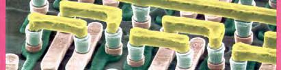
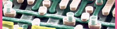
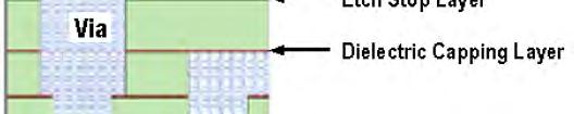
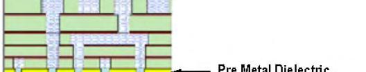
13 A Cross-Section Insulators Interconnects Transistors Tiwari_12_2009_iWSG_Technology.pptx 25 Maxwell s Equations Original Scaled Scaling Factors 26
14 27 Low κ Oxide Density (g/cm 3 ) Dielectric constant (κ) ~ Modulus (GPa) ~ Hardness (GPa) ~ cte (ppm/k) ~ Porosity ~35-65% none Average Pore < nm none Thermal Conductivity (W/m.K) 28
 (110) 1.")
15 Damascene (111) (100) (110) 1.2 μm 29 30
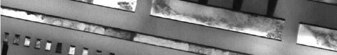
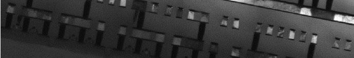
16 Metal Resistivity At <200 nm, Cu Resistance starts to rise Grain boundaries and interface scattering with Ta based barriers 31 Voids and accumulation caused by flux divergence, accelerated by stress and temperature 32


 Metal Voids")
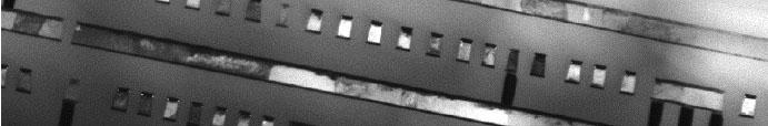
17 Interconnects Passivated Cu: 350 nm, width 600 nm Stress temperature: 230 C Current densities increased up to 10 7 A/cm2 during ~17 hrs Sneider, Fut Fab Vol19 33 Electromigration Technology & Reliability Issues e - Hillocks Nucleation on defects (111) Metal Voids (100) 300 nm 300 nm Before After 34


18 e - Technology & Reliability Issues Voids! Electromigration Low k Diffusion Barrier! (111) Metal Voids Dielectric cracking! Porosity! 300 nm 300 nm 35 Electromigration Drift of atoms in the direction of electron flow caused by fields: electron wind Aluminum: mitigated by alloying with Cu and conductive barrier/liner layers Nernst Equation: Atom drift velocity Effective charge Diffusivity Electromigration driving force Intrinsic atom mobility Field ed resistivity s Current density 36
19 Reliability of Insulators In transistors: thick and thin oxides and consequences of high κ with particular emphasis on NBTI Implications for circuits In Flash Memories implications of relatively thick oxides 37 Gate Dielectric: Nitrided Oxide with polysi Leaky, difficult to control, B penetration, SILC, soft breakdowns, NBTI, PBTI, 38
20 Metal Gates and High κ 39 Plasma Damage Linder, P2ID(1948) Thin Oxides (scaled devices) reduced damage Thick Oxides (IO devices) damage persists New effects at small dimensions: i new dielectrics, i different BEOL dielectrics i and processing techniques (UV cure?) and heavy dose implants 40
21 Old: Charge to Breakdown Defect generation to Breakdown DiMaria, APL(1997) 41 Bias Dependence of Breakdown Growth From 0 to 100 μa breakdown leakage in 300 years of continuous operation J. Stathis (2008) 42


 43")
22 Charge to Breakdown Percolation Stathis, IRPS(2001) and JAP (1999) 43 Stress Induced Leakage Current SILC 44
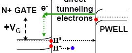
23 Oxides and Transport in Insulators Oid Oxides: The properties of SiO 2 change to bulk like over a length scale of about 2 monolayers. Direct tunneling is certainly quite significant at sizes below about 1.5 nm. What does electron transport do when biases are applied in oxides? Energy losses in the insulator breaking bonds and trapping carriers (so charge in oxides, and sites in oxides through which electron transport can take place (e.g. by percolation) Energy losses at interfaces breaking bonds, releasing ionized species that can then move in applied fields Magnitudes of various effects depend on how thick oxides are, bias conditions and multiple phenomena may be important simultaneously. Effects may be hard, i.e. abrupt or soft, i.e. a gentle degradation 45 Dielectric Reliability: Nitridation Hardening Bulk properties lost below 2 monolayers Below 32 nm, SiON required for appropriate EOT (electrical thickness) is very high in N Power law mechanisms may involve the release of H 0 and dh + from poly-sion interface E. Wu, IEDM(2000) P. Nicollian IRPS (2003) & IEDM(2005) 46

 47")


24 Outline Ultra-thin oxide breakdown Progressive breakdown Circuit it implications Negative Bias Temperature Instability (NBTI) Role of Nitrogen New materials Comments for thick Oxides (NVRAMs) 47 Progressive Breakdown Hard Breakdown doesn t happen suddenly as a catastrophic process Happens gradually over a measurable time scale Degradation rate is slower for lower stress voltages Log time scale Hosoi, IEDM(2002) 48


25 What does it Mean? Thick Oxide High Voltage Stress Ultra-Thin Oxide Low Voltage Stress T. Hosoi, SSDM(2002) 49 Interface State Distribution Mid-gap defects with gated diode peak Conduction band edge defects with flat- band gate leakage (LV-SILC) Stathis, INFOS(2005) 50


26 Interpretation All breakdown is progressive Continuum of rates of post-bd current growth Progressive BD can be stopped at intermediate current level Operational definitions are circuit dependent 51 Negative Bias Positive bias shifts away from the SiO2/Si interface Charge exchange: Hole trapping or electron detrapping increases the net positive charge at the Si/SiO 2 interface 52
27 NBTI: A Serious Reliability Issue pmos threshold shift (drain current reduction) Interface states and positive oxide charge Serious concern for low V DD new technologies Nitridation worsens NBTI 53 Channel Hot Carrier Issues with Scaling Decreasing lifetime L g shrinking while V DD scaling limited Increased use of well bias => additional stress JW McPherson, IEDM(2005) 54
 Thermal activation: ~0.")
28 NBTI Reddy, IRPS(2002) Lower Thermal budget Ox thick. scaling Nitridation SOC Ox thick. scaling BEOL Power dissipation 55 NBTI: Negative Bias Temperature Instability Negative Bias Temperature Instability pfet on-state (holes involved) Thermal activation: ~0.2 ev Miura & Matukura, JJAP(1966) Power law dependence of t n with n ~ Source believed to be electrochemical reaction with a hydrogen related species in the oxide Reaction/diffusion i 56
29 NBTI: Dispersive Transport Zafar, JAP(2005) Hydrogen density calculated from kinetics (is statistical) Creation of interfacial and oxide traps Interfacial and oxide traps have charged and neutral states t Charge state densities follow Fermi function Correct treatment of the drift/diffusion of [H] including dispersive nature of process in amorphous medium Dispersive transport arises when mobile species experiences a broad distribution of barrier heights leading to an exponentially broad distribution of hopping times Causes stretched exponential This reduces to power law form and accounts for saturation at long times at short times, 57 Process Influence Nitridation of gate oxide enhances NBTI Deuterium some publications show improvement Fluorinated gate oxide reduces NBTI Improvement diminishes with nitridation Oxidation conditions and tooling BEOL charging enhances NBTI effect Composition of contact etch stop layer and stress films 58
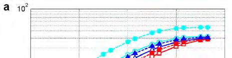

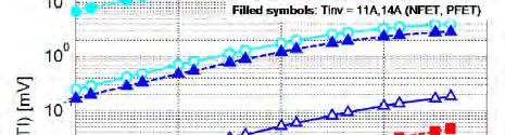
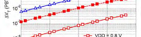
30 Circuit Implications 59 SRAM Increasing asymmetry from NBTI and PBTI PBTI more sensitive to T inv SRAM cell itself more sensitive to NBTI Read affected more than Write A. Bansal, Micro Rel (2009) 60

31 Implications of Progressive Breakdown Many characteristics are not strongly perturbed by oxide breakdown e.g. transconductance (gm) and threshold voltage (V T ) Strongest implication is in an increase in off current in gate-drain or gate-source leakage Include power law equation from breakdown curves 61 Inverter Transfer Characteristics Loads output of 1 st inverter by breakdown in 2 nd Logic may tolerate high breakdown leakage (~10 μa)with reduced noise margin (is another source of variability) 62
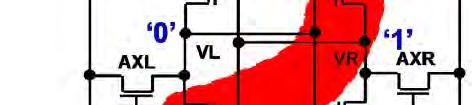
32 SRAM Static Noise Margin At breakdown current > 50 μa, SNM reduced by 50% Worst case: n-source breakdown Pulls down voltage at opposite node Loads a weaker pfet Rodriguez, EDL(2002) 63 Circuit Failure Distribution Follows from Weibull ebu distribution ds of oxide BD times (β=1 for t ox < 2 nm): Assumed exponential distribution of post BD times (Δt): E. Wu, IEDM(2003) 64
33 Circuit Failure Distribution Example: For 100 ppm failure (F=10-4 ) A 100x increase in lifetime 65 High κ 66
34 HfSiON: SiO 2 Shanware, IEDM(2003) 2-3 orders of reduced leakage over SiO2 Carrier mobility is ~20% below universal curve at high fields Thermal stability to 1100 C 67 High κ Breakdown Breakdown strength decreases with κ Field/voltage acceleration g increases with κ (useful in burn-in and stress testing) 68
35 NBTI in High κ Similar to SiO 2 Interface dominated Power law time dependence Saturation Relaxation Dependence on temperature & field Zafar, EDL(2005) 69 High κ Stability Shanware, IEDM(2003) Some of the high κ dielectrics are quite unstable under stress Lower breakdown strength will affect thickness scaling 70


36 HfO 2 /SiO 2 Stack Stressing Two time constants (others have observed three) At the beginning: due to preexisting traps(?) Then, degradation due to stressing A third one, depending on thicknesses, due to hard breakdown E. Amat, Microelectron Rel (2007) 71 Recovery: Metal Gate with high κ Recovery and recovery rate after stressing Interface properties affect ΔV T, but little effect on recovery Stressing field, rather than stressing voltage, influences NBTI recovery in pmosfet M. Wang, Micro Eng (2009) 72
37 Metal Gate 73 FUSI: fully silicided Metal Gates Higher dielectric leakage and reduced breakdown strength with metal gates (FUSI) Electric stressing show higher V T shifts in metal gates Metal gates: Stability of interface under NBTI and PBTI Process impact of charging, breakdown, TDDB Workfunction variability 74
 75 Metal Gate with High κ At <1 μa, progressive breakdown before catastrophic breakdown The increase in stress current just before hard")
38 Metal Gate Breakdown Transients Fast breakdown transients t (i.e. hard breakdown) observed in metal gates FETs in the voltage range where polysi gate show progressive breakdwon Advantage of progressive breakdown lost for metal gates Palumbo, IRPS(2004) 75 Metal Gate with High κ At <1 μa, progressive breakdown before catastrophic breakdown The increase in stress current just before hard breakdown is progressive breakdown since independent of device area and localized in the same position as final hard breakdown S. Lombardo, ISAGST(2006) 76
39 Charge Trapping Dependence on Gate Metal gates are better Silicide is similar to polysi polysi/high κ interactions appear to be prime suspect for charge trapping instabilities in polysi and FUSI devices PBTI has a stretched exponential dependence similar to NBTI Gusev, IEDM(2004) 77 Summary For polysi gates: Hard breakdown is a slow ( progressive ) process : Breakdown criterion is circuit-dependent Circuit failure will be later than initial oxide breakdown For metal gates: Progressive breakdown is less apparent V T stability is a concern for oxynitride and new dielectrics/gates 78
40 Back Up 79 80

41 Clock Span Increasing f clk and speed Reduced logic span Higher electromagnetic coupling: capacitive coupling inductive bounce Source: Saraswat Tiwari_12_2009_iWSG_Technology.pptx 81 Transmission Line V in l l l l r r r x r V out g c g c g c g c The Wave Equation 82
42 Taking the repeater loading into account Repeaters For a given technology and a given interconnect layer, there exists an optimal length of the wire segments between repeaters. The delay of these wire segments is independent of the routing layer: 83 Inductance in Supply Lines ut (V) V ou i L (A) x 10-9 Without inductors With inductors decoupled x x x V L (V) time (nsec) x 10-9 time (nsec) x Input rise/fall time: 50 psec Input rise/fall time: 800 psec 84


 And Oxide progressive")
43 Mitigating Inductive Effects Separation of power pins for I/O pads and core Multiple power and ground pins Careful positioning of the power and ground pins on the package Increase the rise and fall times of the off-chip signals to the maximum extent allowable Schedule current-consuming transitions Improved packaging Add decoupling capacitance 85 SRAM cell Flip Failure Envelope Minimum voltage of SRAM affected by combination of NBTI (pfet VT shift) And Oxide progressive breakdown Mueller, IRPS(2004) 86
44 Metal Gate High κ Major issue Mobility degradation Threshold h voltage control For high κ, electron trapping under positive bias (PBTI in nfet) is a new concern 87
L ECE 4211 UConn F. Jain Scaling Laws for NanoFETs Chapter 10 Logic Gate Scaling
 L13 04202017 ECE 4211 UConn F. Jain Scaling Laws for NanoFETs Chapter 10 Logic Gate Scaling Scaling laws: Generalized scaling (GS) p. 610 Design steps p.613 Nanotransistor issues (page 626) Degradation
Announcements. EE141- Fall 2002 Lecture 25. Interconnect Effects I/O, Power Distribution
 - Fall 2002 Lecture 25 Interconnect Effects I/O, Power Distribution Announcements Homework 9 due next Tuesday Hardware lab this week Project phase 2 due in two weeks 1 Today s Lecture Impact of interconnects»
Negative Bias Temperature Instability (NBTI) Physics, Materials, Process, and Circuit Issues. Dieter K. Schroder Arizona State University Tempe, AZ
 Physics, Materials, Process, and Circuit Issues. Dieter K. Schroder Arizona State University Tempe, AZ") Negative Bias Temperature Instability (NBTI) Physics, Materials, Process, and Circuit Issues Dieter K. Schroder Arizona State University Tempe, AZ Introduction What is NBTI? Material Issues Device Issues
Negative Bias Temperature Instability (NBTI) Physics, Materials, Process, and Circuit Issues Dieter K. Schroder Arizona State University Tempe, AZ Introduction What is NBTI? Material Issues Device Issues
OFF-state TDDB in High-Voltage GaN MIS-HEMTs
 OFF-state TDDB in High-Voltage GaN MIS-HEMTs Shireen Warnock and Jesús A. del Alamo Microsystems Technology Laboratories (MTL) Massachusetts Institute of Technology (MIT) Purpose Further understanding
10/16/2008 GMU, ECE 680 Physical VLSI Design
 ECE680: Physical VLSI Design Chapter VI Coping with Interconnect 1 Impact of Interconnect Parasitics Reduce Robustness Affect Performance Increase delay Increase power dissipation Classes of Parasitics
Lecture 16: Circuit Pitfalls
 Introduction to CMOS VLSI Design Lecture 16: Circuit Pitfalls David Harris Harvey Mudd College Spring 2004 Outline Pitfalls Detective puzzle Given circuit and symptom, diagnose cause and recommend solution
Interconnect (2) Buffering Techniques.Transmission Lines. Lecture Fall 2003
 Buffering Techniques.Transmission Lines. Lecture Fall 2003") Interconnect (2) Buffering Techniques.Transmission Lines Lecture 12 18-322 Fall 2003 A few announcements Partners Lab Due Times Midterm 1 is nearly here Date: 10/14/02, time: 3:00-4:20PM, place: in class
Interconnect (2) Buffering Techniques.Transmission Lines Lecture 12 18-322 Fall 2003 A few announcements Partners Lab Due Times Midterm 1 is nearly here Date: 10/14/02, time: 3:00-4:20PM, place: in class
Lecture 23. Dealing with Interconnect. Impact of Interconnect Parasitics
 Lecture 23 Dealing with Interconnect Impact of Interconnect Parasitics Reduce Reliability Affect Performance Classes of Parasitics Capacitive Resistive Inductive 1 INTERCONNECT Dealing with Capacitance
Lecture 16: Circuit Pitfalls
 Lecture 16: Circuit Pitfalls Outline Variation Noise Budgets Reliability Circuit Pitfalls 2 Variation Process Threshold Channel length Interconnect dimensions Environment Voltage Temperature Aging / Wearout
Interconnects. Wire Resistance Wire Capacitance Wire RC Delay Crosstalk Wire Engineering Repeaters. ECE 261 James Morizio 1
 Interconnects Wire Resistance Wire Capacitance Wire RC Delay Crosstalk Wire Engineering Repeaters ECE 261 James Morizio 1 Introduction Chips are mostly made of wires called interconnect In stick diagram,
VLSI GATE LEVEL DESIGN UNIT - III P.VIDYA SAGAR ( ASSOCIATE PROFESSOR) Department of Electronics and Communication Engineering, VBIT
 Department of Electronics and Communication Engineering, VBIT") VLSI UNIT - III GATE LEVEL DESIGN P.VIDYA SAGAR ( ASSOCIATE PROFESSOR) contents GATE LEVEL DESIGN : Logic Gates and Other complex gates, Switch logic, Alternate gate circuits, Time Delays, Driving large
VLSI UNIT - III GATE LEVEL DESIGN P.VIDYA SAGAR ( ASSOCIATE PROFESSOR) contents GATE LEVEL DESIGN : Logic Gates and Other complex gates, Switch logic, Alternate gate circuits, Time Delays, Driving large
Lecture 21: Packaging, Power, & Clock
 Lecture 21: Packaging, Power, & Clock Outline Packaging Power Distribution Clock Distribution 2 Packages Package functions Electrical connection of signals and power from chip to board Little delay or
Topics to be Covered. capacitance inductance transmission lines
 Topics to be Covered Circuit Elements Switching Characteristics Power Dissipation Conductor Sizes Charge Sharing Design Margins Yield resistance capacitance inductance transmission lines Resistance of
CMPEN 411 VLSI Digital Circuits. Lecture 03: MOS Transistor
 CMPEN 411 VLSI Digital Circuits Lecture 03: MOS Transistor Kyusun Choi [Adapted from Rabaey s Digital Integrated Circuits, Second Edition, 2003 J. Rabaey, A. Chandrakasan, B. Nikolic] CMPEN 411 L03 S.1
Interconnects. Introduction
 Interconnects Wire Resistance Wire Capacitance Wire RC Delay Crosstalk Wire Engineering Repeaters ECE 261 Krish Chakrabarty 1 Introduction Chips are mostly made of ires called interconnect In stick diagram,
MOS Transistor Theory
 MOS Transistor Theory So far, we have viewed a MOS transistor as an ideal switch (digital operation) Reality: less than ideal EE 261 Krish Chakrabarty 1 Introduction So far, we have treated transistors
EE410 vs. Advanced CMOS Structures
 EE410 vs. Advanced CMOS Structures Prof. Krishna S Department of Electrical Engineering S 1 EE410 CMOS Structure P + poly-si N + poly-si Al/Si alloy LPCVD PSG P + P + N + N + PMOS N-substrate NMOS P-well
21. LECTURE 21: INTRODUCTION TO DIELECTRIC BREAKDOWN
 98 21. LECTURE 21: INTRODUCTION TO DIELECTRIC BREAKDOWN 21.1 Review/Background This class is an introduction to Time Dependent Dielectric Breakdown (TDDB). In the following 9 chapters, we will discuss
ENEE 359a Digital VLSI Design
 SLIDE 1 ENEE 359a Digital VLSI Design & Logical Effort Prof. blj@ece.umd.edu Credit where credit is due: Slides contain original artwork ( Jacob 2004) as well as material taken liberally from Irwin & Vijay
EE650R: Reliability Physics of Nanoelectronic Devices Lecture 18: A Broad Introduction to Dielectric Breakdown Date:
 EE650R: Reliability Physics of Nanoelectronic Devices Lecture 18: A Broad Introduction to Dielectric Breakdown Date: Nov 1, 2006 ClassNotes: Jing Li Review: Sayeef Salahuddin 18.1 Review As discussed before,
The Wire EE141. Microelettronica
 The Wire 1 Interconnect Impact on Chip 2 Example: a Bus Network transmitters receivers schematics physical 3 Wire Models All-inclusive model Capacitance-only 4 Impact of Interconnect Parasitics Interconnect
ELEN0037 Microelectronic IC Design. Prof. Dr. Michael Kraft
 ELEN0037 Microelectronic IC Design Prof. Dr. Michael Kraft Lecture 2: Technological Aspects Technology Passive components Active components CMOS Process Basic Layout Scaling CMOS Technology Integrated
MOSFET: Introduction
 E&CE 437 Integrated VLSI Systems MOS Transistor 1 of 30 MOSFET: Introduction Metal oxide semiconductor field effect transistor (MOSFET) or MOS is widely used for implementing digital designs Its major
Stretching the Barriers An analysis of MOSFET Scaling. Presenters (in order) Zeinab Mousavi Stephanie Teich-McGoldrick Aseem Jain Jaspreet Wadhwa
 Zeinab Mousavi Stephanie Teich-McGoldrick Aseem Jain Jaspreet Wadhwa") Stretching the Barriers An analysis of MOSFET Scaling Presenters (in order) Zeinab Mousavi Stephanie Teich-McGoldrick Aseem Jain Jaspreet Wadhwa Why Small? Higher Current Lower Gate Capacitance Higher
Stretching the Barriers An analysis of MOSFET Scaling Presenters (in order) Zeinab Mousavi Stephanie Teich-McGoldrick Aseem Jain Jaspreet Wadhwa Why Small? Higher Current Lower Gate Capacitance Higher
Digital Integrated Circuits A Design Perspective
 Semiconductor Memories Adapted from Chapter 12 of Digital Integrated Circuits A Design Perspective Jan M. Rabaey et al. Copyright 2003 Prentice Hall/Pearson Outline Memory Classification Memory Architectures
ESE 570: Digital Integrated Circuits and VLSI Fundamentals
 ESE 570: Digital Integrated Circuits and VLSI Fundamentals Lec 24: April 19, 2018 Crosstalk and Wiring, Transmission Lines Lecture Outline! Crosstalk! Repeaters in Wiring! Transmission Lines " Where transmission
Power Dissipation. Where Does Power Go in CMOS?
 Power Dissipation [Adapted from Chapter 5 of Digital Integrated Circuits, 2003, J. Rabaey et al.] Where Does Power Go in CMOS? Dynamic Power Consumption Charging and Discharging Capacitors Short Circuit
Lecture 4: CMOS Transistor Theory
 Introduction to CMOS VLSI Design Lecture 4: CMOS Transistor Theory David Harris, Harvey Mudd College Kartik Mohanram and Steven Levitan University of Pittsburgh Outline q Introduction q MOS Capacitor q
Lecture 25. Semiconductor Memories. Issues in Memory
 Lecture 25 Semiconductor Memories Issues in Memory Memory Classification Memory Architectures TheMemoryCore Periphery 1 Semiconductor Memory Classification RWM NVRWM ROM Random Access Non-Random Access
The Physics of Soft-Breakdown and its Implications for Integrated Circuits
 The Physics of Soft-Breakdown and its Implications for Integrated Circuits Muhammad Ashraful Alam in collaboration with B. Weir, P. Silverman, and R. K. Smith Agere Systems, PA 18109 What is Soft-Breakdown
MOS Transistor Theory
 CHAPTER 3 MOS Transistor Theory Outline 2 1. Introduction 2. Ideal I-V Characteristics 3. Nonideal I-V Effects 4. C-V Characteristics 5. DC Transfer Characteristics 6. Switch-level RC Delay Models MOS
A Computational Model of NBTI and Hot Carrier Injection Time-Exponents for MOSFET Reliability
 Journal of Computational Electronics 3: 165 169, 2004 c 2005 Springer Science + Business Media, Inc. Manufactured in The Netherlands. A Computational Model of NBTI and Hot Carrier Injection Time-Exponents
! Crosstalk. ! Repeaters in Wiring. ! Transmission Lines. " Where transmission lines arise? " Lossless Transmission Line.
 ESE 570: Digital Integrated Circuits and VLSI Fundamentals Lec 24: April 19, 2018 Crosstalk and Wiring, Transmission Lines Lecture Outline! Crosstalk! Repeaters in Wiring! Transmission Lines " Where transmission
23.0 Review Introduction
 EE650R: Reliability Physics of Nanoelectronic Devices Lecture 23: TDDB: Measurement of bulk trap density Date: Nov 13 2006 Classnotes: Dhanoop Varghese Review: Nauman Z Butt 23.0 Review In the last few
MOS Transistor I-V Characteristics and Parasitics
 ECEN454 Digital Integrated Circuit Design MOS Transistor I-V Characteristics and Parasitics ECEN 454 Facts about Transistors So far, we have treated transistors as ideal switches An ON transistor passes
Reliability Testing. Process-Related Reliability Tests. Quality and Reliability Report. Non-Volatile Memory Cycling Endurance
 Reliability Testing The purpose of reliability testing is to ensure that products are properly designed and assembled by subjecting them to stress conditions that accelerate potential failure mechanisms.
LECTURE 3 MOSFETS II. MOS SCALING What is Scaling?
 LECTURE 3 MOSFETS II Lecture 3 Goals* * Understand constant field and constant voltage scaling and their effects. Understand small geometry effects for MOS transistors and their implications modeling and
Objective and Outline. Acknowledgement. Objective: Power Components. Outline: 1) Acknowledgements. Section 4: Power Components
 Acknowledgements. Section 4: Power Components") Objective: Power Components Outline: 1) Acknowledgements 2) Objective and Outline 1 Acknowledgement This lecture note has been obtained from similar courses all over the world. I wish to thank all the
Objective: Power Components Outline: 1) Acknowledgements 2) Objective and Outline 1 Acknowledgement This lecture note has been obtained from similar courses all over the world. I wish to thank all the
Negative-Bias Temperature Instability (NBTI) of GaN MOSFETs
 of GaN MOSFETs") Negative-Bias Temperature Instability (NBTI) of GaN MOSFETs Alex Guo and Jesús A. del Alamo Microsystems Technology Laboratories (MTL) Massachusetts Institute of Technology (MIT) Cambridge, MA, USA Sponsor:
Negative-Bias Temperature Instability (NBTI) of GaN MOSFETs Alex Guo and Jesús A. del Alamo Microsystems Technology Laboratories (MTL) Massachusetts Institute of Technology (MIT) Cambridge, MA, USA Sponsor:
EE141-Spring 2008 Digital Integrated Circuits EE141. Announcements EECS141 EE141. Lecture 24: Wires
 EE141-Spring 2008 Digital Integrated Circuits Lecture 24: Wires 1 Announcements Hw 8 posted last graded homework Project phase II feedback to be expected anytime 2 Material Last Lecture: Wire capacitance
Reliability and Instability of GaN MIS-HEMTs for Power Electronics
 Reliability and Instability of GaN MIS-HEMTs for Power Electronics Jesús A. del Alamo, Alex Guo and Shireen Warnock Microsystems Technology Laboratories Massachusetts Institute of Technology 2016 Fall
EE141-Spring 2007 Digital Integrated Circuits. Administrative Stuff. Last Lecture. Wires. Interconnect Impact on Chip. The Wire
 EE141-Spring 2007 Digital Integrated Circuits ecture 10 Administrative Stuff No ab this week Midterm 1 on Tu! HW5 to be posted by next Friday Due Fr. March 2 5pm Introduction to wires 1 2 ast ecture ast
Lecture 5: CMOS Transistor Theory
 Lecture 5: CMOS Transistor Theory Slides courtesy of Deming Chen Slides based on the initial set from David Harris CMOS VLSI Design Outline q q q q q q q Introduction MOS Capacitor nmos I-V Characteristics
CONSTANT CURRENT STRESS OF ULTRATHIN GATE DIELECTRICS
 CONSTANT CURRENT STRESS OF ULTRATHIN GATE DIELECTRICS Y. Sun School of Electrical & Electronic Engineering Nayang Technological University Nanyang Avenue, Singapore 639798 e-mail: 14794258@ntu.edu.sg Keywords:
Digital Integrated Circuits. The Wire * Fuyuzhuo. *Thanks for Dr.Guoyong.SHI for his slides contributed for the talk. Digital IC.
 Digital Integrated Circuits The Wire * Fuyuzhuo *Thanks for Dr.Guoyong.SHI for his slides contributed for the talk Introduction The Wire transmitters receivers schematics physical 2 Interconnect Impact
CMPEN 411 VLSI Digital Circuits Spring 2012
 CMPEN 411 VLSI Digital Circuits Spring 2012 Lecture 09: Resistance & Inverter Dynamic View [Adapted from Rabaey s Digital Integrated Circuits, Second Edition, 2003 J. Rabaey, A. Chandrakasan, B. Nikolic]
VLSI Design and Simulation
 VLSI Design and Simulation Performance Characterization Topics Performance Characterization Resistance Estimation Capacitance Estimation Inductance Estimation Performance Characterization Inverter Voltage
Lecture 12: MOS Capacitors, transistors. Context
 Lecture 12: MOS Capacitors, transistors Context In the last lecture, we discussed PN diodes, and the depletion layer into semiconductor surfaces. Small signal models In this lecture, we will apply those
Chapter 3 Basics Semiconductor Devices and Processing
 Chapter 3 Basics Semiconductor Devices and Processing Hong Xiao, Ph. D. www2.austin.cc.tx.us/hongxiao/book.htm Hong Xiao, Ph. D. www2.austin.cc.tx.us/hongxiao/book.htm 1 Objectives Identify at least two
ENEE 359a Digital VLSI Design
 SLIDE 1 ENEE 359a Digital VLSI Design Prof. blj@eng.umd.edu Credit where credit is due: Slides contain original artwork ( Jacob 2004) as well as material taken liberally from Irwin & Vijay s CSE477 slides
THE INVERTER. Inverter
 THE INVERTER DIGITAL GATES Fundamental Parameters Functionality Reliability, Robustness Area Performance» Speed (delay)» Power Consumption» Energy Noise in Digital Integrated Circuits v(t) V DD i(t) (a)
DKDT: A Performance Aware Dual Dielectric Assignment for Tunneling Current Reduction
 DKDT: A Performance Aware Dual Dielectric Assignment for Tunneling Current Reduction Saraju P. Mohanty Dept of Computer Science and Engineering University of North Texas smohanty@cs.unt.edu http://www.cs.unt.edu/~smohanty/
And device degradation. Slide 1
 And device degradation Slide 1 Z. Guo, ISSSCC 2018 Inter-die Variation & Cell Failures Failures in SRAM Array Overall Cell Failure: [ ] P = P Fail = P A! R! W! H F F F F F P MEM Redundant Columns PASS
The Wire. Digital Integrated Circuits A Design Perspective. Jan M. Rabaey Anantha Chandrakasan Borivoje Nikolic. July 30, 2002
 Digital Integrated Circuits A Design Perspective Jan M. Rabaey Anantha Chandrakasan Borivoje Nikolic The Wire July 30, 2002 1 The Wire transmitters receivers schematics physical 2 Interconnect Impact on
Fig. 1 CMOS Transistor Circuits (a) Inverter Out = NOT In, (b) NOR-gate C = NOT (A or B)
 Inverter Out = NOT In, (b) NOR-gate C = NOT (A or B)") 1 Introduction to Transistor-Level Logic Circuits 1 By Prawat Nagvajara At the transistor level of logic circuits, transistors operate as switches with the logic variables controlling the open or closed
1 Introduction to Transistor-Level Logic Circuits 1 By Prawat Nagvajara At the transistor level of logic circuits, transistors operate as switches with the logic variables controlling the open or closed
Lecture 040 Integrated Circuit Technology - II (5/11/03) Page ECE Frequency Synthesizers P.E. Allen
 Page ECE Frequency Synthesizers P.E. Allen") Lecture 040 Integrated Circuit Technology - II (5/11/03) Page 040-1 LECTURE 040 INTEGRATED CIRCUIT TECHNOLOGY - II (Reference [7,8]) Objective The objective of this presentation is: 1.) Illustrate and
Lecture 040 Integrated Circuit Technology - II (5/11/03) Page 040-1 LECTURE 040 INTEGRATED CIRCUIT TECHNOLOGY - II (Reference [7,8]) Objective The objective of this presentation is: 1.) Illustrate and
Lecture 25. Dealing with Interconnect and Timing. Digital Integrated Circuits Interconnect
 Lecture 25 Dealing with Interconnect and Timing Administrivia Projects will be graded by next week Project phase 3 will be announced next Tu.» Will be homework-like» Report will be combined poster Today
ESE 570: Digital Integrated Circuits and VLSI Fundamentals
 ESE 570: Digital Integrated Circuits and VLSI Fundamentals Lec 23: April 17, 2018 I/O Circuits, Inductive Noise, CLK Generation Lecture Outline! Packaging! Variation and Testing! I/O Circuits! Inductive
SEMICONDUCTOR MEMORIES
 SEMICONDUCTOR MEMORIES Semiconductor Memory Classification RWM NVRWM ROM Random Access Non-Random Access EPROM E 2 PROM Mask-Programmed Programmable (PROM) SRAM FIFO FLASH DRAM LIFO Shift Register CAM
Semiconductor Memories
 Semiconductor References: Adapted from: Digital Integrated Circuits: A Design Perspective, J. Rabaey UCB Principles of CMOS VLSI Design: A Systems Perspective, 2nd Ed., N. H. E. Weste and K. Eshraghian
Announcements. EE141- Fall 2002 Lecture 7. MOS Capacitances Inverter Delay Power
 - Fall 2002 Lecture 7 MOS Capacitances Inverter Delay Power Announcements Wednesday 12-3pm lab cancelled Lab 4 this week Homework 2 due today at 5pm Homework 3 posted tonight Today s lecture MOS capacitances
P. R. Nelson 1 ECE418 - VLSI. Midterm Exam. Solutions
 P. R. Nelson 1 ECE418 - VLSI Midterm Exam Solutions 1. (8 points) Draw the cross-section view for A-A. The cross-section view is as shown below.. ( points) Can you tell which of the metal1 regions is the
EE 466/586 VLSI Design. Partha Pande School of EECS Washington State University
 EE 466/586 VLSI Design Partha Pande School of EECS Washington State University pande@eecs.wsu.edu Lecture 8 Power Dissipation in CMOS Gates Power in CMOS gates Dynamic Power Capacitance switching Crowbar
EECS130 Integrated Circuit Devices
 EECS130 Integrated Circuit Devices Professor Ali Javey 10/30/2007 MOSFETs Lecture 4 Reading: Chapter 17, 19 Announcements The next HW set is due on Thursday. Midterm 2 is next week!!!! Threshold and Subthreshold
10. Performance. Summary
 10. Performance Summary Interconnect Parameters: Capacitance, Resistance, Inductance Electrical Wire Models Lumped C model Lumped RC model RC chain model Distributed RC line model Transmission line model
Digital Integrated Circuits A Design Perspective. Semiconductor. Memories. Memories
 Digital Integrated Circuits A Design Perspective Semiconductor Chapter Overview Memory Classification Memory Architectures The Memory Core Periphery Reliability Case Studies Semiconductor Memory Classification
Interconnect s Role in Deep Submicron. Second class to first class
 Interconnect s Role in Deep Submicron Dennis Sylvester EE 219 November 3, 1998 Second class to first class Interconnect effects are no longer secondary # of wires # of devices More metal levels RC delay
Nanoscale CMOS Design Issues
 Nanoscale CMOS Design Issues Jaydeep P. Kulkarni Assistant Professor, ECE Department The University of Texas at Austin jaydeep@austin.utexas.edu Fall, 2017, VLSI-1 Class Transistor I-V Review Agenda Non-ideal
Power Consumption in CMOS CONCORDIA VLSI DESIGN LAB
 Power Consumption in CMOS 1 Power Dissipation in CMOS Two Components contribute to the power dissipation:» Static Power Dissipation Leakage current Sub-threshold current» Dynamic Power Dissipation Short
Microelectronics Reliability
 Microelectronics Reliability 49 (2009) 642 649 Contents lists available at ScienceDirect Microelectronics Reliability journal homepage: www.elsevier.com/locate/microrel Impacts of NBTI and PBTI on SRAM
MOS Transistors. Prof. Krishna Saraswat. Department of Electrical Engineering Stanford University Stanford, CA
 MOS Transistors Prof. Krishna Saraswat Department of Electrical Engineering S Stanford, CA 94305 saraswat@stanford.edu 1 1930: Patent on the Field-Effect Transistor! Julius Lilienfeld filed a patent describing
CSE493/593. Designing for Low Power
 CSE493/593 Designing for Low Power Mary Jane Irwin [Adapted from Rabaey s Digital Integrated Circuits, 2002, J. Rabaey et al.].1 Why Power Matters Packaging costs Power supply rail design Chip and system
5.0 CMOS Inverter. W.Kucewicz VLSICirciuit Design 1
 5.0 CMOS Inverter W.Kucewicz VLSICirciuit Design 1 Properties Switching Threshold Dynamic Behaviour Capacitance Propagation Delay nmos/pmos Ratio Power Consumption Contents W.Kucewicz VLSICirciuit Design
Chapter 2 CMOS Transistor Theory. Jin-Fu Li Department of Electrical Engineering National Central University Jungli, Taiwan
 Chapter 2 CMOS Transistor Theory Jin-Fu Li Department of Electrical Engineering National Central University Jungli, Taiwan Outline Introduction MOS Device Design Equation Pass Transistor Jin-Fu Li, EE,
ESE 570: Digital Integrated Circuits and VLSI Fundamentals
 ESE 570: Digital Integrated Circuits and VLSI Fundamentals Lec 23: April 13, 2017 Variation; I/O Circuits, Inductive Noise Lecture Outline! Design Quality " Variation! Packaging! Variation and Testing!
Breakdown Characterization
 An Array-Based Test Circuit it for Fully Automated Gate Dielectric Breakdown Characterization John Keane, Shrinivas Venkatraman, Paulo Butzen*, and Chris H. Kim *State University of Rio Grande do Sul,
Section 12: Intro to Devices
 Section 12: Intro to Devices Extensive reading materials on reserve, including Robert F. Pierret, Semiconductor Device Fundamentals EE143 Ali Javey Bond Model of Electrons and Holes Si Si Si Si Si Si Si
MODEL MECHANISM OF CMOS DEVICE FOR RELIBILITY ENHANCEMENT
 MODEL MECHANISM OF CMOS DEVICE FOR RELIBILITY ENHANCEMENT Sandeep Lalawat and Prof.Y.S.Thakur lalawat_er2007@yahoo.co.in,ystgecu@yahoo.co.in Abstract This paper present specific device level life time
CMOS Transistors, Gates, and Wires
 CMOS Transistors, Gates, and Wires Should the hardware abstraction layers make today s lecture irrelevant? pplication R P C W / R W C W / 6.375 Complex Digital Systems Christopher atten February 5, 006
Section 12: Intro to Devices
 Section 12: Intro to Devices Extensive reading materials on reserve, including Robert F. Pierret, Semiconductor Device Fundamentals Bond Model of Electrons and Holes Si Si Si Si Si Si Si Si Si Silicon
CHAPTER 5 EFFECT OF GATE ELECTRODE WORK FUNCTION VARIATION ON DC AND AC PARAMETERS IN CONVENTIONAL AND JUNCTIONLESS FINFETS
 98 CHAPTER 5 EFFECT OF GATE ELECTRODE WORK FUNCTION VARIATION ON DC AND AC PARAMETERS IN CONVENTIONAL AND JUNCTIONLESS FINFETS In this chapter, the effect of gate electrode work function variation on DC
CS 152 Computer Architecture and Engineering
 CS 152 Computer Architecture and Engineering Lecture 12 VLSI II 2005-2-24 John Lazzaro (www.cs.berkeley.edu/~lazzaro) TAs: Ted Hong and David Marquardt www-inst.eecs.berkeley.edu/~cs152/ Last Time: Device
Chapter 2 Characterization Methods for BTI Degradation and Associated Gate Insulator Defects
 Chapter 2 Characterization Methods for BTI Degradation and Associated Gate Insulator Defects Souvik Mahapatra, Nilesh Goel, Ankush Chaudhary, Kaustubh Joshi and Subhadeep Mukhopadhyay Abstract In this
EE105 Fall 2014 Microelectronic Devices and Circuits. NMOS Transistor Capacitances: Saturation Region
 EE105 Fall 014 Microelectronic Devices and Circuits Prof. Ming C. Wu wu@eecs.berkeley.edu 511 Sutardja Dai Hall (SDH) 1 NMOS Transistor Capacitances: Saturation Region Drain no longer connected to channel
Very Large Scale Integration (VLSI)
") Very Large Scale Integration (VLSI) Lecture 4 Dr. Ahmed H. Madian Ah_madian@hotmail.com Dr. Ahmed H. Madian-VLSI Contents Delay estimation Simple RC model Penfield-Rubenstein Model Logical effort Delay
Very Large Scale Integration (VLSI) Lecture 4 Dr. Ahmed H. Madian Ah_madian@hotmail.com Dr. Ahmed H. Madian-VLSI Contents Delay estimation Simple RC model Penfield-Rubenstein Model Logical effort Delay
Properties of CMOS Gates Snapshot
 MOS logic 1 Properties of MOS Gates Snapshot High noise margins: V OH and V OL are at V DD and GND, respectively. No static power consumption: There never exists a direct path between V DD and V SS (GND)
Fundamentals of the Metal Oxide Semiconductor Field-Effect Transistor
 Triode Working FET Fundamentals of the Metal Oxide Semiconductor Field-Effect Transistor The characteristics of energy bands as a function of applied voltage. Surface inversion. The expression for the
Future trends in radiation hard electronics
 Future trends in radiation hard electronics F. Faccio CERN, Geneva, Switzerland Outline Radiation effects in CMOS technologies Deep submicron CMOS for radiation environments What is the future going to
Chapter 2 Process Variability. Overview. 2.1 Sources and Types of Variations
 Chapter 2 Process Variability Overview Parameter variability has always been an issue in integrated circuits. However, comparing with the size of devices, it is relatively increasing with technology evolution,
MSE 310/ECE 340: Electrical Properties of Materials Fall 2014 Department of Materials Science and Engineering Boise State University
 MSE 310/ECE 340: Electrical Properties of Materials Fall 2014 Department of Materials Science and Engineering Boise State University Practice Final Exam 1 Read the questions carefully Label all figures
Timing Simulation of 45 nm Technology and Analysis of Gate Tunneling Currents in 90, 65, 45, and 32 nm Technologies
 1 Timing Simulation of 45 nm Technology and Analysis of Gate Tunneling Currents in 90, 65, 45, and 32 nm Technologies Steven P. Surgnier Abstract A timing simulation is presented for a MOSFET implemented
The CMOS Inverter: A First Glance
 The CMOS Inverter: A First Glance V DD S D V in V out C L D S CMOS Inverter N Well V DD V DD PMOS 2λ PMOS Contacts In Out In Out Metal 1 NMOS Polysilicon NMOS GND CMOS Inverter: Steady State Response V
for Leading Edge CMOS and SiGe Technologies
 1 Reliability IBM Challenges Systems and Technology and Qualification Group - SRDC Methodology for Leading Edge CMOS and SiGe Technologies Fernando Guarín Ph.D IEEE Fellow Semiconductor Research & Development
GMU, ECE 680 Physical VLSI Design 1
 ECE680: Physical VLSI Design Chapter VIII Semiconductor Memory (chapter 12 in textbook) 1 Chapter Overview Memory Classification Memory Architectures The Memory Core Periphery Reliability Case Studies
Digital Integrated Circuits EECS 312
 14 12 10 8 6 Fujitsu VP2000 IBM 3090S Pulsar 4 IBM 3090 IBM RY6 CDC Cyber 205 IBM 4381 IBM RY4 2 IBM 3081 Apache Fujitsu M380 IBM 370 Merced IBM 360 IBM 3033 Vacuum Pentium II(DSIP) 0 1950 1960 1970 1980
Lecture 6 Power Zhuo Feng. Z. Feng MTU EE4800 CMOS Digital IC Design & Analysis 2010
 EE4800 CMOS Digital IC Design & Analysis Lecture 6 Power Zhuo Feng 6.1 Outline Power and Energy Dynamic Power Static Power 6.2 Power and Energy Power is drawn from a voltage source attached to the V DD
 Distributed by: www.jameco.com 1-800-831-4242 The content and copyrights of the attached material are the property of its owner. DS0026 Dual High-Speed MOS Driver General Description DS0026 is a low cost
Low Power VLSI Circuits and Systems Prof. Ajit Pal Department of Computer Science and Engineering Indian Institute of Technology, Kharagpur
 Low Power VLSI Circuits and Systems Prof. Ajit Pal Department of Computer Science and Engineering Indian Institute of Technology, Kharagpur Lecture No. # 08 MOS Inverters - III Hello, and welcome to today
Operation and Modeling of. The MOS Transistor. Second Edition. Yannis Tsividis Columbia University. New York Oxford OXFORD UNIVERSITY PRESS
 Operation and Modeling of The MOS Transistor Second Edition Yannis Tsividis Columbia University New York Oxford OXFORD UNIVERSITY PRESS CONTENTS Chapter 1 l.l 1.2 1.3 1.4 1.5 1.6 1.7 Chapter 2 2.1 2.2
CS/EE N-type Transistor
 CS/EE 6710 MOS Transistor Models Electrical Effects Propagation Delay N-type Transistor D + G Vds i electrons +Vgs S - 1 Another Cutaway View Thanks to National Central University for Some images Vgs Forms