Digital Integrated Circuits. The Wire * Fuyuzhuo. *Thanks for Dr.Guoyong.SHI for his slides contributed for the talk. Digital IC.
|
|
|
- Alaina Gibbs
- 5 years ago
- Views:
Transcription
1 Digital Integrated Circuits The Wire * Fuyuzhuo *Thanks for Dr.Guoyong.SHI for his slides contributed for the talk Introduction
2 The Wire transmitters receivers schematics physical 2

3 Interconnect Impact on Chip 3
4 Wire Models All-inclusive model Capacitance-only 4
5 Impact of Interconnect Parasitics Interconnect parasitics(cap./r./inductive) reduce reliability/performance/power Inductive ignored condition resistance of the wire is substantial enough long metal wire with a small cross section,or if the rise and fall times of the applied signal are slow Wires are short,cross section of the wire is large,or the interconnection has a low resistivity Interwire capacitance ignored condition Separation between neighboring wires is 5
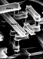
6 Source: Intel Nature of Interconnect Local Interconnect Pentium Pro (R) Pentium(R) II Pentium (MMX) Pentium (R) Pentium (R) II No of nets (Log Scale) S Local = S Technology Global Interconnect S Global = S Die ,000 10, ,000 Length (u) 6
7 INTERCONNECT Capacitance Introduction 7
8 Capacitance of Wire Interconnect V DD V DD V in C gd12 M2 C db2 V out C g4 M4 V out2 M1 C db1 C w Interconnect C g3 M3 Fanout Simplified Model V in V out C L 8

9 Capacitance: The Parallel Plate Model Too simplistic when W/H ratio become small c int t εdi = kε 0 di di WL H t di L W Current flow Dielectric Electrical-field lines k = 3.9 for SiO 2 Processes are starting to use low-k dielectrics k 3 (or less) as dielectrics use air pockets Substrate S Cwire S S S L 1 S L 9
10 Permittivity 10
 H W - H/2 + (b)")
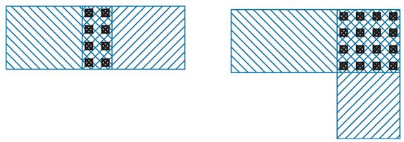
11 Fringing Capacitance Over the years, a steady reduction in the W/H ratio which has even dropped below 1 (a) H W - H/2 + (b) 11

12 Fringing versus Parallel Plate Including fringing cap. Gap (from [Bakoglu89]) 12
13 Interwire Capacitance fringing parallel 13
14 Impact of Interwire Capacitance Interwire capacitance starts to dominate when W becomes smaller than 1.75H (from [Bakoglu89]) 14
 Area cap.")
15 Wiring Capacitances (0.25 mm CMOS) Area cap. af/um2 Fringing cap. af/um 15
16 Example Wire Capacitance Example 4.1: a global clock wire for 1 to 2 cm die size can reach a length of 10 cm. if the wire width is 1um and uses AL1. the wire capacitance is calculated as follows: 16
")
17 MIMI and fringe capacitor Poly-insulator-poly(PIP) Metal-insulator-Metal(MIM) Fringe capacitor 17
18 INTERCONNECT Resisitance Introduction 18
19 Wire Resistance R = L H W H L Sheet Resistance R o W R 1 R 2 19
20 Two conductor with equal R 20
21 Interconnect Resistance 21
22 Example Wire Resistance Example 4.2: A 10 cm long and 1 μm wide aluminum wire is routed on the first aluminum layer. Assuming a sheet resistance for Al of Ω/. The total wire resistance is calculated as follows: 22
23 Resistance Estimation 23
24 Example : Parasitic R&C (1/5) 24

25 Example : Parasitic R&C (2/5) 25
26 Example : Parasitic R&C (3/5) 26
27 Example : Parasitic R&C (4/5) 27

28 Example : Parasitic R&C (4/5) 28
29 Example : Parasitic C (1/5) 29
30 Example : Parasitic C (2/5) 30
31 Example : Parasitic C (3/5) 31
32 Example : Parasitic C (4/5) 32
33 Example : Parasitic C (5/5) 33
34 Interconnect Scaling Effect Assume W (wire width), H (wire thickness), t (oxide thickness) all scaled down by S (S > 1). Assume local wire length L scaled down by S ( S > 1) and global wire scaled up by Sg(Sg< 1). 34
35 Interconnect Design Selective Scaling Try not to scale the wire thickness (H) Better interconnect material Copper (Cu) or silicides (better conductivity) Low-k material (lower capacitance) Advanced interconnect topology more interconnect layers thin-denseat lower layers; fat-widely-spacedat higher layers 35
36 Sheet Resistance 36
37 Modern Interconnect 37
38 Resistor layout Meander structure Undoped high-resistivity polysilicon ohm/square 38
39 Crosstalk Floating line Driven line Miller effect Shielding Routing Low-k interconnect Encoding 39
40 Capacitive Coupling to Floating Line 40

41 Capacitive Crosstalk 41

42 Coupling Disturbance 42

43 Capacitive Coupling to Driven Line A step voltage change on line-x results in a transient on line-y For a step VX= 0->2.5V, VY is first charged to ΔV k = Y τ = τ C Y aggressor victim CXY + C = XY R R 1 1+ k aggressor victim + C Then discharges via R Y to 0 with time const (C (C ΔV Y X X + C XY XY ) ) 43
44 ΔV k Capacitive Coupling to Driven Line A step voltage change on line-x results in a transient on line-y For a step VX= 0->2.5V, VY is first charged to = Y τ = τ C Y aggressor victim CXY + C = XY R R 1 1+ k aggressor victim (C (C ΔV Y X X + C + C XY XY ) ) Aggressor Victim (undriven): 50% Victim (half size driver): 16% Victim (equal size driver): 8% Victim (double size driver): 4% t (ps) 44
45 Design Tips for Crosstalk Avoid floating nodes Floating nodes vulnerable to crosstalk Do not run wires in parallel for too long Increase the rise and fall time if possible Use differential signaling Less sensitive to noise Using shielding wires or layers to isolate signal lines 45

46 Shielding 46

47 Miller Effect of Crosstalk Delay depends on activity in neighboring wires When aggressor & victim lines switch in opposite directions, there exists Miller effect. 47
48 Impact of Crosstalk on Delay 48
49 Avoid Crosstalk by Encoding Delay variation is reduced to 2%. Area & capacitance increase by 5%. 49
![Interconnect Organization Dense Wire Fabric ([Kathri2001]) Wires on adjacent layers are routed orthogonally.](/docs-images/82/85897915/images/50-0.jpg "Signals on the same layer are separated by VDD and GND shields(used in FPGAs) V = V DD, S = Signal, G = GND")
50 Interconnect Organization Dense Wire Fabric ([Kathri2001]) Wires on adjacent layers are routed orthogonally. Signals on the same layer are separated by VDD and GND shields(used in FPGAs) V = V DD, S = Signal, G = GND 50
51 Interconnect Modeling 51
52 The Lumped C Model V out Driver c wire C lumped dv dt out V R out V driver in 0 V out ( t) (1 e t ) V, R driver C lumped R driver V out t pd = RCln 2 = 0.69RC = R'C V in C lumped 52
53 Lumped RC Model 53

54 Elmore Delay of RC-Network 54

55 Delay Elmore Delay Another Solution 55
56 Elmore Delay of RC Chain 56
57 Distributed versus Lumped 57
58 Distributed RC Distributed RC-line 58
59 Distributed Wire Model 59
60 Step Step-response of Diffusion response of Diffusion Eqn 60
61 Lumped vs Distributed Models Table 4-7 Step Response of Lumped and Distributed RC Networks: Points of Interest 61
62 Lumped & Distributed Together 62

63 example 63
64 Delay 64
(15625Π)=781ohm. The total capacitance is (0.2fF/um).")
65 Example Consider a 5mm long, 0.32um wide metal2 wire in a 180nm process. The sheet resistance is 0.05ohm/sheet and the capacitance is 0.2fF/um. Construct a 3-segment π-model for the wire Solution:The wire is 5000um/0.32um=15625 squares in length. The total resistance is (0.05ohm/Π)(15625Π)=781ohm. The total capacitance is (0.2fF/um).5000um=1pF. Each π-segment has onethird of this resistance and capacitance. The π-model is shown 65

66 Example -elmore model RC tree Figure shows a gate driving wires to two destinations. The gate is represented as a voltage source with effective resistance R1. the two receivers are located at nodes 3 and 4. the wire to node 3 is long enough that it is represented with a pair of π-segments, while the wire to node 4 is represented with a single segment. Find the Elmore delay from input x to each receiver The Elmore delays are T D3 =R 1 C 1 +(R 1 +R 2 )C 2 +(R 1 +R 2 +R 3 )C 3 +R 1 C 4 T D4 =R 1 C 1 +R 1 C 2 +R 1 C 3 +(R 1 +R 4 )C 4 66

67 Design rules 67
68 A close solution Delay time is τ ( V Break chain and Insert buffer n ) n CR k 0 eq k CR eq n( n 1) 2 68
69 Transmission gate delay optimization Total delay time Assume all has n transmission gate,break chain every m switchs,buffer delay time is t buf t p 0.69[ 0.69CR n m eq m( m 1) CReq ] ( 2 n( m 1) n ( 1) t 2 m n m buf 1) t buf 69

70 Optimal number of switch m optimal m optimal t p m t p 0 m n ntbuf 0.69CReq 2 2 m tbuf CR eq 0 It is independent with n 70

71 Samsung DDR-3 4Gb 71
72 homework 72
The Wire. Digital Integrated Circuits A Design Perspective. Jan M. Rabaey Anantha Chandrakasan Borivoje Nikolic. July 30, 2002
 Digital Integrated Circuits A Design Perspective Jan M. Rabaey Anantha Chandrakasan Borivoje Nikolic The Wire July 30, 2002 1 The Wire transmitters receivers schematics physical 2 Interconnect Impact on
Digital Integrated Circuits (83-313) Lecture 5: Interconnect. Semester B, Lecturer: Adam Teman TAs: Itamar Levi, Robert Giterman 1
 Lecture 5: Interconnect. Semester B, Lecturer: Adam Teman TAs: Itamar Levi, Robert Giterman 1") Digital Integrated Circuits (83-313) Lecture 5: Interconnect Semester B, 2015-16 Lecturer: Adam Teman TAs: Itamar Levi, Robert Giterman 1 What will we learn today? 1 A First Glance at Interconnect 2 3
Digital Integrated Circuits (83-313) Lecture 5: Interconnect Semester B, 2015-16 Lecturer: Adam Teman TAs: Itamar Levi, Robert Giterman 1 What will we learn today? 1 A First Glance at Interconnect 2 3
Lecture 9: Interconnect
 Digital Integrated Circuits (83-313) Lecture 9: Interconnect Semester B, 2016-17 Lecturer: Dr. Adam Teman TAs: Itamar Levi, Robert Giterman 23 May 2017 Disclaimer: This course was prepared, in its entirety,
The Wire EE141. Microelettronica
 The Wire 1 Interconnect Impact on Chip 2 Example: a Bus Network transmitters receivers schematics physical 3 Wire Models All-inclusive model Capacitance-only 4 Impact of Interconnect Parasitics Interconnect
Interconnects. Wire Resistance Wire Capacitance Wire RC Delay Crosstalk Wire Engineering Repeaters. ECE 261 James Morizio 1
 Interconnects Wire Resistance Wire Capacitance Wire RC Delay Crosstalk Wire Engineering Repeaters ECE 261 James Morizio 1 Introduction Chips are mostly made of wires called interconnect In stick diagram,
EE141-Spring 2007 Digital Integrated Circuits. Administrative Stuff. Last Lecture. Wires. Interconnect Impact on Chip. The Wire
 EE141-Spring 2007 Digital Integrated Circuits ecture 10 Administrative Stuff No ab this week Midterm 1 on Tu! HW5 to be posted by next Friday Due Fr. March 2 5pm Introduction to wires 1 2 ast ecture ast
CMPEN 411 VLSI Digital Circuits Spring 2012
 CMPEN 411 VLSI Digital Circuits Spring 2012 Lecture 09: Resistance & Inverter Dynamic View [Adapted from Rabaey s Digital Integrated Circuits, Second Edition, 2003 J. Rabaey, A. Chandrakasan, B. Nikolic]
Interconnects. Introduction
 Interconnects Wire Resistance Wire Capacitance Wire RC Delay Crosstalk Wire Engineering Repeaters ECE 261 Krish Chakrabarty 1 Introduction Chips are mostly made of ires called interconnect In stick diagram,
Integrated Circuits & Systems
 Federal University of Santa Catarina Center for Technology Computer Science & Electronics Engineering Integrated Circuits & Systems INE 5442 Lecture 7 Interconnections 1: wire resistance, capacitance,
Capacitance - 1. The parallel plate capacitor. Capacitance: is a measure of the charge stored on each plate for a given voltage such that Q=CV
 Capacitance - 1 The parallel plate capacitor Capacitance: is a measure of the charge stored on each plate for a given voltage such that Q=CV Charge separation in a parallel-plate capacitor causes an internal
EECS 151/251A Spring 2018 Digital Design and Integrated Circuits. Instructors: Nick Weaver & John Wawrzynek. Lecture 12 EE141
 EECS 151/251A Spring 2018 Digital Design and Integrated Circuits Instructors: Nick Weaver & John Wawrzynek Lecture 12 1 Wire Models All-inclusive model Capacitance-only 2 Capacitance Capacitance: The Parallel
ECE260B CSE241A Winter Interconnects. Website:
 ECE260B CSE241A Winter 2004 Interconnects Website: http://vlsicad.ucsd.edu/courses/ece260b-w04 ECE 260B CSE 241A Interconnects 1 Outline Interconnects Resistance Capacitance and Inductance Delay ECE 260B
VLSI GATE LEVEL DESIGN UNIT - III P.VIDYA SAGAR ( ASSOCIATE PROFESSOR) Department of Electronics and Communication Engineering, VBIT
 Department of Electronics and Communication Engineering, VBIT") VLSI UNIT - III GATE LEVEL DESIGN P.VIDYA SAGAR ( ASSOCIATE PROFESSOR) contents GATE LEVEL DESIGN : Logic Gates and Other complex gates, Switch logic, Alternate gate circuits, Time Delays, Driving large
VLSI UNIT - III GATE LEVEL DESIGN P.VIDYA SAGAR ( ASSOCIATE PROFESSOR) contents GATE LEVEL DESIGN : Logic Gates and Other complex gates, Switch logic, Alternate gate circuits, Time Delays, Driving large
Lecture 23. Dealing with Interconnect. Impact of Interconnect Parasitics
 Lecture 23 Dealing with Interconnect Impact of Interconnect Parasitics Reduce Reliability Affect Performance Classes of Parasitics Capacitive Resistive Inductive 1 INTERCONNECT Dealing with Capacitance
CARNEGIE MELLON UNIVERSITY DEPARTMENT OF ELECTRICAL AND COMPUTER ENGINEERING DIGITAL INTEGRATED CIRCUITS FALL 2002
 CARNEGIE MELLON UNIVERSITY DEPARTMENT OF ELECTRICAL AND COMPUTER ENGINEERING 18-322 DIGITAL INTEGRATED CIRCUITS FALL 2002 Final Examination, Monday Dec. 16, 2002 NAME: SECTION: Time: 180 minutes Closed
EE141-Spring 2008 Digital Integrated Circuits EE141. Announcements EECS141 EE141. Lecture 24: Wires
 EE141-Spring 2008 Digital Integrated Circuits Lecture 24: Wires 1 Announcements Hw 8 posted last graded homework Project phase II feedback to be expected anytime 2 Material Last Lecture: Wire capacitance
ECE520 VLSI Design. Lecture 8: Interconnect Manufacturing and Modeling. Payman Zarkesh-Ha
 ECE520 VLSI Design Lecture 8: Interconnect Manufacturing and Modeling Payman Zarkesh-Ha Office: ECE Bldg. 230B Office hours: Wednesday 2:00-3:00PM or by appointment E-mail: pzarkesh@unm.edu Slide: 1 Review
ESE 570: Digital Integrated Circuits and VLSI Fundamentals
 ESE 570: Digital Integrated Circuits and VLSI Fundamentals Lec 24: April 19, 2018 Crosstalk and Wiring, Transmission Lines Lecture Outline! Crosstalk! Repeaters in Wiring! Transmission Lines " Where transmission
! Crosstalk. ! Repeaters in Wiring. ! Transmission Lines. " Where transmission lines arise? " Lossless Transmission Line.
 ESE 570: Digital Integrated Circuits and VLSI Fundamentals Lec 24: April 19, 2018 Crosstalk and Wiring, Transmission Lines Lecture Outline! Crosstalk! Repeaters in Wiring! Transmission Lines " Where transmission
VLSI Design and Simulation
 VLSI Design and Simulation Performance Characterization Topics Performance Characterization Resistance Estimation Capacitance Estimation Inductance Estimation Performance Characterization Inverter Voltage
CPE/EE 427, CPE 527 VLSI Design I L13: Wires, Design for Speed. Course Administration
 CPE/EE 427, CPE 527 VLSI Design I L3: Wires, Design for Speed Department of Electrical and Computer Engineering University of labama in Huntsville leksandar Milenkovic ( www.ece.uah.edu/~milenka ) www.ece.uah.edu/~milenka/cpe527-05f
Digital Integrated Circuits A Design Perspective
 Semiconductor Memories Adapted from Chapter 12 of Digital Integrated Circuits A Design Perspective Jan M. Rabaey et al. Copyright 2003 Prentice Hall/Pearson Outline Memory Classification Memory Architectures
Lecture 12 CMOS Delay & Transient Response
 EE 471: Transport Phenomena in Solid State Devices Spring 2018 Lecture 12 CMOS Delay & Transient Response Bryan Ackland Department of Electrical and Computer Engineering Stevens Institute of Technology
Announcements. EE141- Fall 2002 Lecture 25. Interconnect Effects I/O, Power Distribution
 - Fall 2002 Lecture 25 Interconnect Effects I/O, Power Distribution Announcements Homework 9 due next Tuesday Hardware lab this week Project phase 2 due in two weeks 1 Today s Lecture Impact of interconnects»
Very Large Scale Integration (VLSI)
") Very Large Scale Integration (VLSI) Lecture 4 Dr. Ahmed H. Madian Ah_madian@hotmail.com Dr. Ahmed H. Madian-VLSI Contents Delay estimation Simple RC model Penfield-Rubenstein Model Logical effort Delay
Very Large Scale Integration (VLSI) Lecture 4 Dr. Ahmed H. Madian Ah_madian@hotmail.com Dr. Ahmed H. Madian-VLSI Contents Delay estimation Simple RC model Penfield-Rubenstein Model Logical effort Delay
Topics to be Covered. capacitance inductance transmission lines
 Topics to be Covered Circuit Elements Switching Characteristics Power Dissipation Conductor Sizes Charge Sharing Design Margins Yield resistance capacitance inductance transmission lines Resistance of
Lecture 7 Circuit Delay, Area and Power
 Lecture 7 Circuit Delay, Area and Power lecture notes from S. Mitra Intro VLSI System course (EE271) Introduction to VLSI Systems 1 Circuits and Delay Introduction to VLSI Systems 2 Power, Delay and Area:
EE115C Digital Electronic Circuits Homework #5
 EE115C Digital Electronic Circuits Homework #5 Due Thursday, May 13, 6pm @ 56-147E EIV Problem 1 Elmore Delay Analysis Calculate the Elmore delay from node A to node B using the values for the resistors
Lecture 4: CMOS Transistor Theory
 Introduction to CMOS VLSI Design Lecture 4: CMOS Transistor Theory David Harris, Harvey Mudd College Kartik Mohanram and Steven Levitan University of Pittsburgh Outline q Introduction q MOS Capacitor q
THE INVERTER. Inverter
 THE INVERTER DIGITAL GATES Fundamental Parameters Functionality Reliability, Robustness Area Performance» Speed (delay)» Power Consumption» Energy Noise in Digital Integrated Circuits v(t) V DD i(t) (a)
Spiral 2 7. Capacitance, Delay and Sizing. Mark Redekopp
 2-7.1 Spiral 2 7 Capacitance, Delay and Sizing Mark Redekopp 2-7.2 Learning Outcomes I understand the sources of capacitance in CMOS circuits I understand how delay scales with resistance, capacitance
GMU, ECE 680 Physical VLSI Design 1
 ECE680: Physical VLSI Design Chapter VIII Semiconductor Memory (chapter 12 in textbook) 1 Chapter Overview Memory Classification Memory Architectures The Memory Core Periphery Reliability Case Studies
ENEE 359a Digital VLSI Design
 SLIDE 1 ENEE 359a Digital VLSI Design & Logical Effort Prof. blj@ece.umd.edu Credit where credit is due: Slides contain original artwork ( Jacob 2004) as well as material taken liberally from Irwin & Vijay
Semiconductor Memories
 Semiconductor References: Adapted from: Digital Integrated Circuits: A Design Perspective, J. Rabaey UCB Principles of CMOS VLSI Design: A Systems Perspective, 2nd Ed., N. H. E. Weste and K. Eshraghian
Interconnect s Role in Deep Submicron. Second class to first class
 Interconnect s Role in Deep Submicron Dennis Sylvester EE 219 November 3, 1998 Second class to first class Interconnect effects are no longer secondary # of wires # of devices More metal levels RC delay
ECE260B CSE241A Winter Interconnects. Website:
 ECE260B CSE241A Winter 2007 Interconnects Website: http://vlsicad.ucsd.edu/courses/ece260b-w07 ECE 260B CSE 241A Interconnects 1 Outline Interconnect Scaling and Power Resistance Capacitance and Inductance
10/16/2008 GMU, ECE 680 Physical VLSI Design
 ECE680: Physical VLSI Design Chapter VI Coping with Interconnect 1 Impact of Interconnect Parasitics Reduce Robustness Affect Performance Increase delay Increase power dissipation Classes of Parasitics
Digital Integrated Circuits A Design Perspective. Semiconductor. Memories. Memories
 Digital Integrated Circuits A Design Perspective Semiconductor Chapter Overview Memory Classification Memory Architectures The Memory Core Periphery Reliability Case Studies Semiconductor Memory Classification
Lecture 5: DC & Transient Response
 Lecture 5: DC & Transient Response Outline q Pass Transistors q DC Response q Logic Levels and Noise Margins q Transient Response q RC Delay Models q Delay Estimation 2 Activity 1) If the width of a transistor
Interconnect (2) Buffering Techniques.Transmission Lines. Lecture Fall 2003
 Buffering Techniques.Transmission Lines. Lecture Fall 2003") Interconnect (2) Buffering Techniques.Transmission Lines Lecture 12 18-322 Fall 2003 A few announcements Partners Lab Due Times Midterm 1 is nearly here Date: 10/14/02, time: 3:00-4:20PM, place: in class
Interconnect (2) Buffering Techniques.Transmission Lines Lecture 12 18-322 Fall 2003 A few announcements Partners Lab Due Times Midterm 1 is nearly here Date: 10/14/02, time: 3:00-4:20PM, place: in class
Homework #2 10/6/2016. C int = C g, where 1 t p = t p0 (1 + C ext / C g ) = t p0 (1 + f/ ) f = C ext /C g is the effective fanout
 = t p0 (1 + f/ ) f = C ext /C g is the effective fanout") 0/6/06 Homework # Lecture 8, 9: Sizing and Layout of omplex MOS Gates Reading: hapter 4, sections 4.3-4.5 October 3 & 5, 06 hapter, section.5.5 Prof. R. Iris ahar Weste & Harris vailable on course webpage
0/6/06 Homework # Lecture 8, 9: Sizing and Layout of omplex MOS Gates Reading: hapter 4, sections 4.3-4.5 October 3 & 5, 06 hapter, section.5.5 Prof. R. Iris ahar Weste & Harris vailable on course webpage
5.0 CMOS Inverter. W.Kucewicz VLSICirciuit Design 1
 5.0 CMOS Inverter W.Kucewicz VLSICirciuit Design 1 Properties Switching Threshold Dynamic Behaviour Capacitance Propagation Delay nmos/pmos Ratio Power Consumption Contents W.Kucewicz VLSICirciuit Design
The Inverter. Digital Integrated Circuits A Design Perspective. Jan M. Rabaey Anantha Chandrakasan Borivoje Nikolic
 Digital Integrated Circuits A Design Perspective Jan M. Rabaey Anantha Chandrakasan Borivoje Nikolic The Inverter Revised from Digital Integrated Circuits, Jan M. Rabaey el, 2003 Propagation Delay CMOS
10. Performance. Summary
 10. Performance Summary Interconnect Parameters: Capacitance, Resistance, Inductance Electrical Wire Models Lumped C model Lumped RC model RC chain model Distributed RC line model Transmission line model
MOS Transistor Theory
 MOS Transistor Theory So far, we have viewed a MOS transistor as an ideal switch (digital operation) Reality: less than ideal EE 261 Krish Chakrabarty 1 Introduction So far, we have treated transistors
Integrated Circuits & Systems
 Federal University of Santa Catarina Center for Technology Computer Science & Electronics Engineering Integrated Circuits & Systems INE 5442 Lecture 14 The CMOS Inverter: dynamic behavior (sizing, inverter
The Physical Structure (NMOS)
") The Physical Structure (NMOS) Al SiO2 Field Oxide Gate oxide S n+ Polysilicon Gate Al SiO2 SiO2 D n+ L channel P Substrate Field Oxide contact Metal (S) n+ (G) L W n+ (D) Poly 1 Transistor Resistance Two
The Physical Structure (NMOS) Al SiO2 Field Oxide Gate oxide S n+ Polysilicon Gate Al SiO2 SiO2 D n+ L channel P Substrate Field Oxide contact Metal (S) n+ (G) L W n+ (D) Poly 1 Transistor Resistance Two
SEMICONDUCTOR MEMORIES
 SEMICONDUCTOR MEMORIES Semiconductor Memory Classification RWM NVRWM ROM Random Access Non-Random Access EPROM E 2 PROM Mask-Programmed Programmable (PROM) SRAM FIFO FLASH DRAM LIFO Shift Register CAM
The CMOS Inverter: A First Glance
 The CMOS Inverter: A First Glance V DD V in V out C L CMOS Properties Full rail-to-rail swing Symmetrical VTC Propagation delay function of load capacitance and resistance of transistors No static power
CMOS Transistors, Gates, and Wires
 CMOS Transistors, Gates, and Wires Should the hardware abstraction layers make today s lecture irrelevant? pplication R P C W / R W C W / 6.375 Complex Digital Systems Christopher atten February 5, 006
ESE 570: Digital Integrated Circuits and VLSI Fundamentals
 ESE 570: Digital Integrated Circuits and VLSI Fundamentals Lec 15: March 3, 2016 Combination Logic: Ratioed & Pass Logic, and Performance Lecture Outline! CMOS NOR2 Worst Case Analysis! Pass Transistor
9/18/2008 GMU, ECE 680 Physical VLSI Design
 ECE680: Physical VLSI Design Chapter III CMOS Device, Inverter, Combinational circuit Logic and Layout Part 3 Combinational Logic Gates (textbook chapter 6) 9/18/2008 GMU, ECE 680 Physical VLSI Design
The CMOS Inverter: A First Glance
 The CMOS Inverter: A First Glance V DD S D V in V out C L D S CMOS Inverter N Well V DD V DD PMOS 2λ PMOS Contacts In Out In Out Metal 1 NMOS Polysilicon NMOS GND CMOS Inverter: Steady State Response V
Circuits. L5: Fabrication and Layout -2 ( ) B. Mazhari Dept. of EE, IIT Kanpur. B. Mazhari, IITK. G-Number
 B. Mazhari Dept. of EE, IIT Kanpur. B. Mazhari, IITK. G-Number") EE610: CMOS Analog Circuits L5: Fabrication and Layout -2 (12.8.2013) B. Mazhari Dept. of EE, IIT Kanpur 44 Passive Components: Resistor Besides MOS transistors, sometimes one requires to implement passive
EE610: CMOS Analog Circuits L5: Fabrication and Layout -2 (12.8.2013) B. Mazhari Dept. of EE, IIT Kanpur 44 Passive Components: Resistor Besides MOS transistors, sometimes one requires to implement passive
Lecture 4: DC & Transient Response
 Introduction to CMOS VLSI Design Lecture 4: DC & Transient Response David Harris Harvey Mudd College Spring 004 Outline DC Response Logic Levels and Noise Margins Transient Response Delay Estimation Slide
Hw 6 and 7 Graded and available Project Phase 2 Graded Project Phase 3 Launch Today
 EECS141 1 Hw 8 Posted Last one to be graded Due Friday April 30 Hw 6 and 7 Graded and available Project Phase 2 Graded Project Phase 3 Launch Today EECS141 2 1 6 5 4 3 2 1 0 1.5 2 2.5 3 3.5 4 Frequency
EE141- Fall 2002 Lecture 27. Memory EE141. Announcements. We finished all the labs No homework this week Projects are due next Tuesday 9am EE141
 - Fall 2002 Lecture 27 Memory Announcements We finished all the labs No homework this week Projects are due next Tuesday 9am 1 Today s Lecture Memory:» SRAM» DRAM» Flash Memory 2 Floating-gate transistor
UNIVERSITY OF CALIFORNIA College of Engineering Department of Electrical Engineering and Computer Sciences. Professor Oldham Fall 1999
 UNIVERSITY OF CLIFORNI College of Engineering Department of Electrical Engineering and Computer Sciences Professor Oldham Fall 1999 EECS 40 FINL EXM 13 December 1999 Name: Last, First Student ID: T: Kusuma
ELEN0037 Microelectronic IC Design. Prof. Dr. Michael Kraft
 ELEN0037 Microelectronic IC Design Prof. Dr. Michael Kraft Lecture 2: Technological Aspects Technology Passive components Active components CMOS Process Basic Layout Scaling CMOS Technology Integrated
EE115C Digital Electronic Circuits Homework #6
 Problem 1 Sizing of adder blocks Electrical Engineering Department Spring 2010 EE115C Digital Electronic Circuits Homework #6 Solution Figure 1: Mirror adder. Study the mirror adder cell (textbook, pages
Next, we check the race condition to see if the circuit will work properly. Note that the minimum logic delay is a single sum.
 UNIVERSITY OF CALIFORNIA College of Engineering Department of Electrical Engineering and Computer Sciences Last modified on May 1, 2003 by Dejan Markovic (dejan@eecs.berkeley.edu) Prof. Jan Rabaey EECS
DC and Transient. Courtesy of Dr. Daehyun Dr. Dr. Shmuel and Dr.
 DC and Transient Courtesy of Dr. Daehyun Lim@WSU, Dr. Harris@HMC, Dr. Shmuel Wimer@BIU and Dr. Choi@PSU http://csce.uark.edu +1 (479) 575-604 yrpeng@uark.edu Pass Transistors We have assumed source is
CS/EE N-type Transistor
 CS/EE 6710 MOS Transistor Models Electrical Effects Propagation Delay N-type Transistor D + G Vds i electrons +Vgs S - 1 Another Cutaway View Thanks to National Central University for Some images Vgs Forms
MOSFET: Introduction
 E&CE 437 Integrated VLSI Systems MOS Transistor 1 of 30 MOSFET: Introduction Metal oxide semiconductor field effect transistor (MOSFET) or MOS is widely used for implementing digital designs Its major
Homework Assignment #5 EE 477 Spring 2017 Professor Parker
 Homework Assignment #5 EE 477 Spring 2017 Professor Parker Question 1: (15%) Compute the worst-case rising and falling RC time constants at point B of the circuit below using the Elmore delay method. Assume
CMOS logic gates. João Canas Ferreira. March University of Porto Faculty of Engineering
 CMOS logic gates João Canas Ferreira University of Porto Faculty of Engineering March 2016 Topics 1 General structure 2 General properties 3 Cell layout João Canas Ferreira (FEUP) CMOS logic gates March
ECE 497 JS Lecture - 18 Noise in Digital Circuits
 ECE 497 JS Lecture - 18 Noise in Digital Circuits Spring 2004 Jose E. Schutt-Aine Electrical & Computer Engineering University of Illinois jose@emlab.uiuc.edu 1 Announcements Thursday April 15 th Speaker:
Lecture 6: DC & Transient Response
 Lecture 6: DC & Transient Response Slides courtesy of Deming Chen Slides based on the initial set from David Harris CMOS VLSI Design Outline Pass Transistors DC Response Logic Levels and Noise Margins
Integrated Circuits & Systems
 Federal University of Santa Catarina Center for Technology Computer Science & Electronics Engineering Integrated Circuits & Systems INE 5442 Lecture 13 The CMOS Inverter: dynamic behavior (delay) guntzel@inf.ufsc.br
EEC 216 Lecture #3: Power Estimation, Interconnect, & Architecture. Rajeevan Amirtharajah University of California, Davis
 EEC 216 Lecture #3: Power Estimation, Interconnect, & Architecture Rajeevan Amirtharajah University of California, Davis Outline Announcements Review: PDP, EDP, Intersignal Correlations, Glitching, Top
Digital Integrated Circuits EECS 312. Review. Fringe vs. parallel plate capacitance. Rent s rule. Impact of inter-wire capacitance
 4 8 6 IM ES9 ipolar Fujitsu VP IM 9S Pulsar 4 IM 9 IM RY6 D yber 5 IM 48 IM RY4 IM 8 pache Fujitsu M8 IM 7 Merced IM 6 IM Vacuum Pentium II(DSIP) 95 96 97 98 99 NTT Fujitsu M-78 Year of announcement IM
Lecture Outline. ESE 570: Digital Integrated Circuits and VLSI Fundamentals. Review: 1st Order RC Delay Models. Review: Two-Input NOR Gate (NOR2)
") ESE 570: Digital Integrated Circuits and VLSI Fundamentals Lec 14: March 1, 2016 Combination Logic: Ratioed and Pass Logic Lecture Outline! CMOS Gates Review " CMOS Worst Case Analysis! Ratioed Logic Gates!
ESE 570: Digital Integrated Circuits and VLSI Fundamentals Lec 14: March 1, 2016 Combination Logic: Ratioed and Pass Logic Lecture Outline! CMOS Gates Review " CMOS Worst Case Analysis! Ratioed Logic Gates!
and V DS V GS V T (the saturation region) I DS = k 2 (V GS V T )2 (1+ V DS )
 I DS = k 2 (V GS V T )2 (1+ V DS )") ECE 4420 Spring 2005 Page 1 FINAL EXAMINATION NAME SCORE /100 Problem 1O 2 3 4 5 6 7 Sum Points INSTRUCTIONS: This exam is closed book. You are permitted four sheets of notes (three of which are your sheets
ECE 4420 Spring 2005 Page 1 FINAL EXAMINATION NAME SCORE /100 Problem 1O 2 3 4 5 6 7 Sum Points INSTRUCTIONS: This exam is closed book. You are permitted four sheets of notes (three of which are your sheets
Lecture 25. Semiconductor Memories. Issues in Memory
 Lecture 25 Semiconductor Memories Issues in Memory Memory Classification Memory Architectures TheMemoryCore Periphery 1 Semiconductor Memory Classification RWM NVRWM ROM Random Access Non-Random Access
Low Power VLSI Circuits and Systems Prof. Ajit Pal Department of Computer Science and Engineering Indian Institute of Technology, Kharagpur
 Low Power VLSI Circuits and Systems Prof. Ajit Pal Department of Computer Science and Engineering Indian Institute of Technology, Kharagpur Lecture No. # 08 MOS Inverters - III Hello, and welcome to today
Lecture #39. Transistor Scaling
 Lecture #39 ANNOUNCEMENT Pick up graded HW assignments and exams (78 Cory) Lecture #40 will be the last formal lecture. Class on Friday will be dedicated to a course review (with sample problems). Discussion
EE382M-14 CMOS Analog Integrated Circuit Design
 EE382M-14 CMOS Analog Integrated Circuit Design Lecture 3, MOS Capacitances, Passive Components, and Layout of Analog Integrated Circuits MOS Capacitances Type of MOS transistor capacitors Depletion capacitance
ECE 497 JS Lecture - 18 Impact of Scaling
 ECE 497 JS Lecture - 18 Impact of Scaling Spring 2004 Jose E. Schutt-Aine Electrical & Computer Engineering University of Illinois jose@emlab.uiuc.edu 1 Announcements Thursday April 8 th Speaker: Prof.
University of Pennsylvania Department of Electrical Engineering. ESE 570 Midterm Exam March 14, 2013 FORMULAS AND DATA
 University of Pennsylvania Department of Electrical Engineering ESE 570 Midterm Exam March 4, 03 FORMULAS AND DATA. PHYSICAL CONSTANTS: n i = intrinsic concentration undoped) silicon =.45 x 0 0 cm -3 @
DesignConEast 2005 Track 4: Power and Packaging (4-WA1)
") DesignConEast 2005 Track 4: Power and Packaging (4-WA1) Design of a Low-Power Differential Repeater Using Low-Voltage Swing and Charge Recycling Authors: Brock J. LaMeres, University of Colorado / Sunil
DesignConEast 2005 Track 4: Power and Packaging (4-WA1) Design of a Low-Power Differential Repeater Using Low-Voltage Swing and Charge Recycling Authors: Brock J. LaMeres, University of Colorado / Sunil
CMOS Cross Section. EECS240 Spring Dimensions. Today s Lecture. Why Talk About Passives? EE240 Process
 EECS240 Spring 202 CMOS Cross Section Metal p - substrate p + diffusion Lecture 2: CMOS Technology and Passive Devices Poly n - well n + diffusion Elad Alon Dept. of EECS EECS240 Lecture 2 4 Today s Lecture
MOSFET and CMOS Gate. Copy Right by Wentai Liu
 MOSFET and CMOS Gate CMOS Inverter DC Analysis - Voltage Transfer Curve (VTC) Find (1) (2) (3) (4) (5) (6) V OH min, V V OL min, V V IH min, V V IL min, V OHmax OLmax IHmax ILmax NM L = V ILmax V OL max
A capacitor is a device that stores electric charge (memory devices). A capacitor is a device that stores energy E = Q2 2C = CV 2
. A capacitor is a device that stores energy E = Q2 2C = CV 2") Capacitance: Lecture 2: Resistors and Capacitors Capacitance (C) is defined as the ratio of charge (Q) to voltage (V) on an object: C = Q/V = Coulombs/Volt = Farad Capacitance of an object depends on geometry
Capacitance: Lecture 2: Resistors and Capacitors Capacitance (C) is defined as the ratio of charge (Q) to voltage (V) on an object: C = Q/V = Coulombs/Volt = Farad Capacitance of an object depends on geometry
Lecture 5: DC & Transient Response
 Lecture 5: DC & Transient Response Outline Pass Transistors DC Response Logic Levels and Noise Margins Transient Response RC Delay Models Delay Estimation 2 Pass Transistors We have assumed source is grounded
Digital Microelectronic Circuits ( )
") Digital Microelectronic ircuits (361-1-3021 ) Presented by: Dr. Alex Fish Lecture 5: Parasitic apacitance and Driving a Load 1 Motivation Thus far, we have learned how to model our essential building block,
Digital Microelectronic ircuits (361-1-3021 ) Presented by: Dr. Alex Fish Lecture 5: Parasitic apacitance and Driving a Load 1 Motivation Thus far, we have learned how to model our essential building block,
EE5780 Advanced VLSI CAD
 EE5780 Advanced VLSI CAD Lecture 4 DC and Transient Responses, Circuit Delays Zhuo Feng 4.1 Outline Pass Transistors DC Response Logic Levels and Noise Margins Transient Response RC Delay Models Delay
EECS240 Spring Today s Lecture. Lecture 2: CMOS Technology and Passive Devices. Lingkai Kong EECS. EE240 CMOS Technology
 EECS240 Spring 2013 Lecture 2: CMOS Technology and Passive Devices Lingkai Kong EECS Today s Lecture EE240 CMOS Technology Passive devices Motivation Resistors Capacitors (Inductors) Next time: MOS transistor
Digital Integrated Circuits EECS 312. Midterm exam 1 II. Homework 3 walkthrough. Review. Rent s rule. Inter-wire capacitance
 8 6 IM ES9 ipolar Fujitsu VP IM 9S NTT Fujitsu M-78 IM 9 D yber 5 Year of announcement IM RY5 IM RY7 Pulsar IM RY6 IM RY MOS Jayhawk(dual) T-Rex Mckinley IM GP Prescott Squadrons IM 9 Pentium IM 8 IM 8
Fig. 1 CMOS Transistor Circuits (a) Inverter Out = NOT In, (b) NOR-gate C = NOT (A or B)
 Inverter Out = NOT In, (b) NOR-gate C = NOT (A or B)") 1 Introduction to Transistor-Level Logic Circuits 1 By Prawat Nagvajara At the transistor level of logic circuits, transistors operate as switches with the logic variables controlling the open or closed
1 Introduction to Transistor-Level Logic Circuits 1 By Prawat Nagvajara At the transistor level of logic circuits, transistors operate as switches with the logic variables controlling the open or closed
Semiconductor memories
 Semiconductor memories Semiconductor Memories Data in Write Memory cell Read Data out Some design issues : How many cells? Function? Power consuption? Access type? How fast are read/write operations? Semiconductor
EE 560 CHIP INPUT AND OUTPUT (I/0) CIRCUITS. Kenneth R. Laker, University of Pennsylvania
 CIRCUITS. Kenneth R. Laker, University of Pennsylvania") 1 EE 560 CHIP INPUT AND OUTPUT (I/0) CIRCUITS 2 -> ESD PROTECTION CIRCUITS (INPUT PADS) -> ON-CHIP CLOCK GENERATION & DISTRIBUTION -> OUTPUT PADS -> ON-CHIP NOISE DUE TO PARASITIC INDUCTANCE -> SUPER BUFFER
1 EE 560 CHIP INPUT AND OUTPUT (I/0) CIRCUITS 2 -> ESD PROTECTION CIRCUITS (INPUT PADS) -> ON-CHIP CLOCK GENERATION & DISTRIBUTION -> OUTPUT PADS -> ON-CHIP NOISE DUE TO PARASITIC INDUCTANCE -> SUPER BUFFER
Switched-Capacitor Circuits David Johns and Ken Martin University of Toronto
 Switched-Capacitor Circuits David Johns and Ken Martin University of Toronto (johns@eecg.toronto.edu) (martin@eecg.toronto.edu) University of Toronto 1 of 60 Basic Building Blocks Opamps Ideal opamps usually
Electrical Characterization of 3D Through-Silicon-Vias
 Electrical Characterization of 3D Through-Silicon-Vias F. Liu, X. u, K. A. Jenkins, E. A. Cartier, Y. Liu, P. Song, and S. J. Koester IBM T. J. Watson Research Center Yorktown Heights, NY 1598, USA Phone:
University of Toronto. Final Exam
 University of Toronto Final Exam Date - Apr 18, 011 Duration:.5 hrs ECE334 Digital Electronics Lecturer - D. Johns ANSWER QUESTIONS ON THESE SHEETS USING BACKS IF NECESSARY 1. Equation sheet is on last
Fundamentals of ANALOG TO DIGITAL CONVERTERS: Part I.3. Technology
 Fundamentals of ANALOG TO DIGITAL CONVERTERS: Part I.3 Technology January 019 Texas A&M University 1 Spring, 019 Well-Diffusion Resistor Example shows two long resistors for K range Alternatively, serpentine
Analysis of TSV-to-TSV Coupling with High-Impedance Termination in 3D ICs
 Analysis of -to- Coupling with -Impedance Termination in 3D ICs Taigon Song, Chang Liu, Dae Hyun Kim, and Sung Kyu Lim School of Electrical and Computer Engineering, Georgia Institute of Technology, U.S.A.
VLSI Design I; A. Milenkovic 1
 ourse dministration PE/EE 47, PE 57 VLSI Design I L3: Wires, Design for Speed Department of Electrical and omputer Engineering University of labama in Huntsville leksandar Milenkovic (.ece.uah.edu/~milenka
Practice 7: CMOS Capacitance
 Practice 7: CMOS Capacitance Digital Electronic Circuits Semester A 2012 MOSFET Capacitances MOSFET Capacitance Components 3 Gate to Channel Capacitance In general, the gate capacitance is similar to a
EECS 141: FALL 05 MIDTERM 1
 University of California College of Engineering Department of Electrical Engineering and Computer Sciences D. Markovic TuTh 11-1:3 Thursday, October 6, 6:3-8:pm EECS 141: FALL 5 MIDTERM 1 NAME Last SOLUTION
LAYOUT TECHNIQUES. Dr. Ivan Grech
 LAYOUT TECHNIQUES OUTLINE Transistor Layout Resistor Layout Capacitor Layout Floor planning Mixed A/D Layout Automatic Analog Layout Layout Techniques Main Layers in a typical Double-Poly, Double-Metal