Lecture 21: Packaging, Power, & Clock
|
|
|
- Edgar Banks
- 6 years ago
- Views:
Transcription

1 Lecture 21: Packaging, Power, & Clock
2 Outline Packaging Power Distribution Clock Distribution 2
3 Packages Package functions Electrical connection of signals and power from chip to board Little delay or distortion Mechanical connection of chip to board Removes heat produced on chip Protects chip from mechanical damage Compatible with thermal expansion Inexpensive to manufacture and test 3

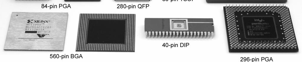
4 Package Types Through-hole vs. surface mount 4
5 Chip-to-Package Bonding Traditionally, chip is surrounded by pad frame Metal pads on μm pitch Gold bond wires attach pads to package Lead frame distributes signals in package Metal heat spreader helps with cooling 5
6 Advanced Packages Bond wires contribute parasitic inductance Fancy packages have many signal, power layers Like tiny printed circuit boards Flip-chip places connections across surface of die rather than around periphery Top level metal pads covered with solder balls Chip flips upside down Carefully aligned to package (done blind!) Heated to melt balls Also called C4 (Controlled Collapse Chip Connection) 6
7 Package Parasitics Use many V DD, GND in parallel Inductance, I DD Package Signal Pins Signal Pads Chip Chip V DD Chip GND Bond Wire Lead Frame Package Capacitor Board V DD Board GND 7
8 Heat Dissipation 60 W light bulb has surface area of 120 cm 2 Itanium 2 die dissipates 130 W over 4 cm 2 Chips have enormous power densities Cooling is a serious challenge Package spreads heat to larger surface area Heat sinks may increase surface area further Fans increase airflow rate over surface area Liquid cooling used in extreme cases ($$$) 8
9 Thermal Resistance ΔT = θ ja P ΔT: temperature rise on chip θ ja : thermal resistance of chip junction to ambient P: power dissipation on chip Thermal resistances combine like resistors Series and parallel θ ja = θ jp + θ pa Series combination 9
10 Example Your chip has a heat sink with a thermal resistance to the package of 4.0 C/W. The resistance from chip to package is 1 C/W. The system box ambient temperature may reach 55 C. The chip temperature must not exceed 100 C. What is the maximum chip power dissipation? ( C) / (4 + 1 C/W) = 9 W 10

11 Temperature Sensor Monitor die temperature and throttle performance if it gets too hot Use a pair of pnp bipolar transistors Vertical pnp available in CMOS qv BE I = I e V = kt c s BE kt ln q I I c s kt I I kt I kt Δ VBE = VBE1 VBE 2 = = = m q I I q I q c1 c2 c1 ln ln ln ln s s c2 Voltage difference is proportional to absolute temp Measure with on-chip A/D converter 11
12 Power Distribution Power Distribution Network functions Carry current from pads to transistors on chip Maintain stable voltage with low noise Provide average and peak power demands Provide current return paths for signals Avoid electromigration & self-heating wearout Consume little chip area and wire Easy to lay out 12
13 Power Requirements V DD = V DDnominal V droop Want V droop < +/- 10% of V DD Sources of V droop IR drops L di/dt noise I DD changes on many time scales Power Max clock gating Average Min Time 13
14 IR Drop A chip draws 24 W from a 1.2 V supply. The power supply impedance is 5 mω. What is the IR drop? I DD = 24 W / 1.2 V = 20 A IR drop = (20 A)(5 mω) = 100 mv 14
15 L di/dt Noise A 1.2 V chip switches from an idle mode consuming 5W to a full-power mode consuming 53 W. The transition takes 10 clock cycles at 1 GHz. The supply inductance is 0.1 nh. What is the L di/dt droop? ΔI = (53 W 5 W)/(1.2 V) = 40 A Δt = 10 cycles * (1 ns / cycle) = 10 ns L di/dt droop = (0.1 nh) * (40 A / 10 ns) = 0.4 V 15
16 Bypass Capacitors Need low supply impedance at all frequencies Ideal capacitors have impedance decreasing with ω Real capacitors have parasitic R and L Leads to resonant frequency of capacitor Ω 1 μf 0.25 nh impedance frequency (Hz) 16
17 Power System Model Power comes from regulator on system board Board and package add parasitic R and L Bypass capacitors help stabilize supply voltage But capacitors also have parasitic R and L Simulate system for time and frequency responses Voltage Regulator Printed Circuit Board Planes Package and Pins Solder Bumps Chip V DD Bulk Capacitor Ceramic Capacitor Package Capacitor On-Chip Capacitor On-Chip Current Demand Board Package 17
18 Frequency Response Multiple capacitors in parallel Large capacitor near regulator has low impedance at low frequencies But also has a low self-resonant frequency Small capacitors near chip and on chip have low impedance at high frequencies Choose caps to get low impedance at all frequencies impedance frequency (Hz) 18
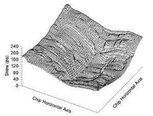
19 Example: Pentium 4 Power supply impedance for Pentium 4 Spike near 100 MHz caused by package L Step response to sudden supply current chain 1 st droop: on-chip bypass caps 2 nd droop: package capacitance 3 rd droop: board capacitance [Xu08] [Wong06] 19
20 Charge Pumps Sometimes a different supply voltage is needed but little current is required 20 V for Flash memory programming Negative body bias for leakage control during sleep Generate the voltage on-chip with a charge pump 20
21 Energy Scavenging Ultra-low power systems can scavenge their energy from the environment rather than needing batteries Solar calculator (solar cells) RFID tags (antenna) Tire pressure monitors powered by vibrational energy of tires (piezoelectric generator) Thin film microbatteries deposited on the chip can store energy for times of peak demand 21
22 Clock Distribution On a small chip, the clock distribution network is just a wire And possibly an inverter for clkb On practical chips, the RC delay of the wire resistance and gate load is very long Variations in this delay cause clock to get to different elements at different times This is called clock skew Most chips use repeaters to buffer the clock and equalize the delay Reduces but doesn t eliminate skew 22
23 Example Skew comes from differences in gate and wire delay With right buffer sizing, clk 1 and clk 2 could ideally arrive at the same time. But power supply noise changes buffer delays clk 2 and clk 3 will always see RC skew 3 mm gclk 3.1 mm 0.5 mm clk pf clk 2 clk pf 0.4 pf 23
24 Review: Skew Impact Ideally full cycle is available for work Skew adds sequencing overhead Increases hold time too F1 clk Q1 D2 clk clk Q1 t pcq Combinational Logic T c t pdq D2 t setup clk F2 t skew ( setup skew ) tpd Tc tpcq + t + t sequencing overhead F1 D2 Q1 clk F2 CL t t t + t cd hold ccq skew clk t skew t hold Q1 t ccq D2 t cd 24
25 Solutions Reduce clock skew Careful clock distribution network design Plenty of metal wiring resources Analyze clock skew Only budget actual, not worst case skews Local vs. global skew budgets Tolerate clock skew Choose circuit structures insensitive to skew 25
26 Clock Dist. Networks Ad hoc Grids H-tree Hybrid 26
27 Clock Grids Use grid on two or more levels to carry clock Make wires wide to reduce RC delay Ensures low skew between nearby points But possibly large skew across die 27


28 Alpha Clock Grids Alpha Alpha Alpha PLL gclk grid gclk grid Alpha Alpha Alpha
29 H-Trees Fractal structure Gets clock arbitrarily close to any point Matched delay along all paths Delay variations cause skew A and B might see big skew A B 29

30 Itanium 2 H-Tree Four levels of buffering: Primary driver Repeater Second-level clock buffer Gater Route around obstructions Repeaters Typical SLCB Locations Primary Buffer 30
31 Hybrid Networks Use H-tree to distribute clock to many points Tie these points together with a grid Ex: IBM Power4, PowerPC H-tree drives sector buffers Buffers drive total of 1024 points All points shorted together with grid 31
Lecture 9: Clocking, Clock Skew, Clock Jitter, Clock Distribution and some FM
 Lecture 9: Clocking, Clock Skew, Clock Jitter, Clock Distribution and some FM Mark McDermott Electrical and Computer Engineering The University of Texas at Austin 9/27/18 VLSI-1 Class Notes Why Clocking?
ESE 570: Digital Integrated Circuits and VLSI Fundamentals
 ESE 570: Digital Integrated Circuits and VLSI Fundamentals Lec 23: April 17, 2018 I/O Circuits, Inductive Noise, CLK Generation Lecture Outline! Packaging! Variation and Testing! I/O Circuits! Inductive
EE 560 CHIP INPUT AND OUTPUT (I/0) CIRCUITS. Kenneth R. Laker, University of Pennsylvania
 CIRCUITS. Kenneth R. Laker, University of Pennsylvania") 1 EE 560 CHIP INPUT AND OUTPUT (I/0) CIRCUITS 2 -> ESD PROTECTION CIRCUITS (INPUT PADS) -> ON-CHIP CLOCK GENERATION & DISTRIBUTION -> OUTPUT PADS -> ON-CHIP NOISE DUE TO PARASITIC INDUCTANCE -> SUPER BUFFER
1 EE 560 CHIP INPUT AND OUTPUT (I/0) CIRCUITS 2 -> ESD PROTECTION CIRCUITS (INPUT PADS) -> ON-CHIP CLOCK GENERATION & DISTRIBUTION -> OUTPUT PADS -> ON-CHIP NOISE DUE TO PARASITIC INDUCTANCE -> SUPER BUFFER
Announcements. EE141- Fall 2002 Lecture 25. Interconnect Effects I/O, Power Distribution
 - Fall 2002 Lecture 25 Interconnect Effects I/O, Power Distribution Announcements Homework 9 due next Tuesday Hardware lab this week Project phase 2 due in two weeks 1 Today s Lecture Impact of interconnects»
Lecture 23. Dealing with Interconnect. Impact of Interconnect Parasitics
 Lecture 23 Dealing with Interconnect Impact of Interconnect Parasitics Reduce Reliability Affect Performance Classes of Parasitics Capacitive Resistive Inductive 1 INTERCONNECT Dealing with Capacitance
PRODUCTION DATA SHEET
 The positive voltage linear regulator is configured with a fixed 3.3V output, featuring low dropout, tight line, load and thermal regulation. VOUT is controlled and predictable as UVLO and output slew
RP mA, Ultra-Low Noise, Ultra-Fast CMOS LDO Regulator. General Description. Features. Applications. Ordering Information. Marking Information
 RP122 3mA, Ultra-Low Noise, Ultra-Fast CMOS LDO Regulator General Description The RP122 is designed for portable RF and wireless applications with demanding performance and space requirements. The RP122
Clock signal in digital circuit is responsible for synchronizing the transfer to the data between processing elements.
 1 2 Introduction Clock signal in digital circuit is responsible for synchronizing the transfer to the data between processing elements. Defines the precise instants when the circuit is allowed to change
CSE241 VLSI Digital Circuits Winter Lecture 07: Timing II
 CSE241 VLSI Digital Circuits Winter 2003 Lecture 07: Timing II CSE241 L3 ASICs.1 Delay Calculation Cell Fall Cap\Tr 0.05 0.2 0.5 0.01 0.02 0.16 0.30 0.5 2.0 0.04 0.32 0.178 0.08 0.64 0.60 1.20 0.1ns 0.147ns
Topics to be Covered. capacitance inductance transmission lines
 Topics to be Covered Circuit Elements Switching Characteristics Power Dissipation Conductor Sizes Charge Sharing Design Margins Yield resistance capacitance inductance transmission lines Resistance of
Spiral 2 7. Capacitance, Delay and Sizing. Mark Redekopp
 2-7.1 Spiral 2 7 Capacitance, Delay and Sizing Mark Redekopp 2-7.2 Learning Outcomes I understand the sources of capacitance in CMOS circuits I understand how delay scales with resistance, capacitance
FPF1003A / FPF1004 IntelliMAX Advanced Load Management Products
 August 2012 FPF1003A / FPF1004 IntelliMAX Advanced Load Management Products Features 1.2 V to 5.5 V Input Voltage Operating Range Typical R DS(ON) : - 30 mω at V IN =5.5 V - 35 mω at V IN =3.3 V ESD Protected:
EE115C Winter 2017 Digital Electronic Circuits. Lecture 19: Timing Analysis
 EE115C Winter 2017 Digital Electronic Circuits Lecture 19: Timing Analysis Outline Timing parameters Clock nonidealities (skew and jitter) Impact of Clk skew on timing Impact of Clk jitter on timing Flip-flop-
Interconnect s Role in Deep Submicron. Second class to first class
 Interconnect s Role in Deep Submicron Dennis Sylvester EE 219 November 3, 1998 Second class to first class Interconnect effects are no longer secondary # of wires # of devices More metal levels RC delay
Lecture 25. Dealing with Interconnect and Timing. Digital Integrated Circuits Interconnect
 Lecture 25 Dealing with Interconnect and Timing Administrivia Projects will be graded by next week Project phase 3 will be announced next Tu.» Will be homework-like» Report will be combined poster Today
SC1301A/B. 2A High Speed Low-Side MOSFET Driver in SOT-23 POWER MANAGEMENT. Applications. Typical Application Circuit
 查询 SC1301B 供应商 Description The is a cost effective single-channel highspeed MOSFET driver. The driver is capable of driving a 1000pF load in 0ns rise/fall time and has a 60ns propagation delay time from
 Distributed by: www.jameco.com 1-800-831-4242 The content and copyrights of the attached material are the property of its owner. September 2001 S7C256 5V/3.3V 32K X 8 CMOS SRM (Common I/O) Features S7C256
PT5108. High-PSRR 500mA LDO GENERAL DESCRIPTION FEATURES APPLICATIONS TYPICAL APPLICATIONS. Ripple Rejection vs Frequency. Ripple Rejection (db)
") GENERAL DESCRIPTION The PT5108 is a low-dropout voltage regulator designed for portable applications that require both low noise performance and board space. Its PSRR at 1kHz is better than 70dB. The PT5108
GENERAL DESCRIPTION The PT5108 is a low-dropout voltage regulator designed for portable applications that require both low noise performance and board space. Its PSRR at 1kHz is better than 70dB. The PT5108
TC ma, Tiny CMOS LDO With Shutdown. General Description. Features. Applications. Package Types SOT-23 SC-70
 1 ma, Tiny CMOS LDO With Shutdown Features Space-saving -Pin SC-7 and SOT-23 Packages Extremely Low Operating Current for Longer Battery Life: 3 µa (typ.) Very Low Dropout Voltage Rated 1 ma Output Current
ESE 570: Digital Integrated Circuits and VLSI Fundamentals
 ESE 570: Digital Integrated Circuits and VLSI Fundamentals Lec 24: April 19, 2018 Crosstalk and Wiring, Transmission Lines Lecture Outline! Crosstalk! Repeaters in Wiring! Transmission Lines " Where transmission
 Distributed by: www.jameco.com 1-800-831-4242 The content and copyrights of the attached material are the property of its owner. DS0026 Dual High-Speed MOS Driver General Description DS0026 is a low cost
MCP9700/9700A MCP9701/9701A
 Low-Power Linear Active Thermistor ICs Features Tiny Analog Temperature Sensor Available Packages: SC-70-5, SOT-23-5, TO-92-3 Wide Temperature Measurement Range: - -40 C to +125 C Accuracy: - ±2 C (max.),
Miniature Electronically Trimmable Capacitor V DD. Maxim Integrated Products 1
 19-1948; Rev 1; 3/01 Miniature Electronically Trimmable Capacitor General Description The is a fine-line (geometry) electronically trimmable capacitor (FLECAP) programmable through a simple digital interface.
FAN ma, Low-IQ, Low-Noise, LDO Regulator
 April 2014 FAN25800 500 ma, Low-I Q, Low-Noise, LDO Regulator Features V IN: 2.3 V to 5.5 V V OUT = 3.3 V (I OUT Max. = 500 ma) V OUT = 5.14 V (I OUT Max. = 250 ma) Output Noise Density at 250 ma and 10
Jin-Fu Li Advanced Reliable Systems (ARES) Lab. Department of Electrical Engineering. Jungli, Taiwan
 Lab. Department of Electrical Engineering. Jungli, Taiwan") Chapter 7 Sequential Circuits Jin-Fu Li Advanced Reliable Systems (ARES) Lab. epartment of Electrical Engineering National Central University it Jungli, Taiwan Outline Latches & Registers Sequencing Timing
Chapter 7 Sequential Circuits Jin-Fu Li Advanced Reliable Systems (ARES) Lab. epartment of Electrical Engineering National Central University it Jungli, Taiwan Outline Latches & Registers Sequencing Timing
! Crosstalk. ! Repeaters in Wiring. ! Transmission Lines. " Where transmission lines arise? " Lossless Transmission Line.
 ESE 570: Digital Integrated Circuits and VLSI Fundamentals Lec 24: April 19, 2018 Crosstalk and Wiring, Transmission Lines Lecture Outline! Crosstalk! Repeaters in Wiring! Transmission Lines " Where transmission
PART. Maxim Integrated Products 1
 9-79; Rev ; 9/ SC7 Inverting Charge Pumps General Description The / monolithic, CMOS chargepump voltage inverters in the ultra-small SC7 package feature a low Ω output resistance, permitting loads up to
10/16/2008 GMU, ECE 680 Physical VLSI Design
 ECE680: Physical VLSI Design Chapter VI Coping with Interconnect 1 Impact of Interconnect Parasitics Reduce Robustness Affect Performance Increase delay Increase power dissipation Classes of Parasitics
DS0026 Dual High-Speed MOS Driver
 Dual High-Speed MOS Driver General Description DS0026 is a low cost monolithic high speed two phase MOS clock driver and interface circuit. Unique circuit design provides both very high speed operation
EMC Considerations for DC Power Design
 EMC Considerations for DC Power Design Tzong-Lin Wu, Ph.D. Department of Electrical Engineering National Sun Yat-sen University Power Bus Noise below 5MHz 1 Power Bus Noise below 5MHz (Solution) Add Bulk
Rg2 Lg2 Rg6 Lg6 Rg7 Lg7. PCB Trace & Plane. Figure 1 Bypass Decoupling Loop
 TECHNICAL NOTE This article was originally published in 1996. INTRODUCTION In order to guarantee better performance from highspeed digital integrated circuits (ICs), manufacturers are tightening power
Compact, Dual-Output Charge Pump
 9-7; Rev ; 7/97 Compact, Dual-Output Charge Pump General Description The is a CMOS charge-pump DC-DC converter in an ultra-small µmax package. It produces positive and negative outputs from a single positive
EE 466/586 VLSI Design. Partha Pande School of EECS Washington State University
 EE 466/586 VLSI Design Partha Pande School of EECS Washington State University pande@eecs.wsu.edu Lecture 8 Power Dissipation in CMOS Gates Power in CMOS gates Dynamic Power Capacitance switching Crowbar
SHM-14 Ultra-Fast, 14-Bit Linear Monolithic Sample-Hold Amplifiers
 INNOVATION and EX C ELL E N C E Ultra-Fast, 1-Bit Linear Monolithic Sample-Hold Amplifiers FEATURES Fast acquisition time: 10ns to ±0.1% 0ns to ±0.0% ns to ±0.01% ±0.001% Nonlinearity 6µV rms output noise
SRAM System Design Guidelines
 Introduction This application note examines some of the important system design considerations an engineer should keep in mind when designing with Cypress SRAMs. It is important to note that while they
CMPEN 411 VLSI Digital Circuits Spring 2012 Lecture 17: Dynamic Sequential Circuits And Timing Issues
 CMPEN 411 VLSI Digital Circuits Spring 2012 Lecture 17: Dynamic Sequential Circuits And Timing Issues [Adapted from Rabaey s Digital Integrated Circuits, Second Edition, 2003 J. Rabaey, A. Chandrakasan,
EE371 - Advanced VLSI Circuit Design
 EE371 - Advanced VLSI Circuit Design Midterm Examination May 7, 2002 Name: No. Points Score 1. 18 2. 22 3. 30 TOTAL / 70 In recognition of and in the spirit of the Stanford University Honor Code, I certify
2 Input NAND Gate L74VHC1G00
 Input NAND Gate The is an advanced high speed CMOS input NAND gate fabricated with silicon gate CMOS technology. It achieves high speed operation similar to equivalent Bipolar Schottky TTL while maintaining
SC70, 1.6V, Nanopower, Beyond-the-Rails Comparators With/Without Reference
 19-1862; Rev 4; 1/7 SC7, 1.6V, Nanopower, Beyond-the-Rails General Description The nanopower comparators in space-saving SC7 packages feature Beyond-the- Rails inputs and are guaranteed to operate down
UNISONIC TECHNOLOGIES CO., LTD L16B45 Preliminary CMOS IC
 UNISONIC TECHNOLOGIES CO., LTD L16B45 Preliminary CMOS IC 16-BIT CONSTANT CURRENT LED SINK DRIVER DESCRIPTION The UTC L16B45 is designed for LED displays. UTC L16B45 contains a serial buffer and data latches
University of Toronto. Final Exam
 University of Toronto Final Exam Date - Apr 18, 011 Duration:.5 hrs ECE334 Digital Electronics Lecturer - D. Johns ANSWER QUESTIONS ON THESE SHEETS USING BACKS IF NECESSARY 1. Equation sheet is on last
GM4275 GM4275 V2.03. Features. Description. Applications. Block Diagram WIDE INPUT RANGE 5V LOW DROPOUT REGULATOR WITH RESET FLAG
 Description The GM4275 series of fixed output, micro-power voltage regulators is designed for applications which require wide input voltage range up to 45V. The GM4275 is an excellent choice for the use
Interconnect (2) Buffering Techniques.Transmission Lines. Lecture Fall 2003
 Buffering Techniques.Transmission Lines. Lecture Fall 2003") Interconnect (2) Buffering Techniques.Transmission Lines Lecture 12 18-322 Fall 2003 A few announcements Partners Lab Due Times Midterm 1 is nearly here Date: 10/14/02, time: 3:00-4:20PM, place: in class
Interconnect (2) Buffering Techniques.Transmission Lines Lecture 12 18-322 Fall 2003 A few announcements Partners Lab Due Times Midterm 1 is nearly here Date: 10/14/02, time: 3:00-4:20PM, place: in class
NTE74HC109 Integrated Circuit TTL High Speed CMOS, Dual J K Positive Edge Triggered Flip Flop w/set & Reset
 NTE74HC109 Integrated Circuit TTL High Speed CMOS, Dual J K Positive Edge Triggered Flip Flop w/set & Reset Description: The NTE74HC109 is a dual J K flip flip with set and reset in a 16 Lead plastic DIP
P4C164 ULTRA HIGH SPEED 8K X 8 STATIC CMOS RAMS FEATURES DESCRIPTION. Full CMOS, 6T Cell. Common Data I/O
 FEATURES Full CMOS, 6T Cell High Speed (Equal Access and Cycle Times) 8/10/12/15/20/25/35/70/100 ns (Commercial) 10/12/15/20/25/35/70/100 ns(industrial) 12/15/20/25/35/45/70/100 ns (Military) Low Power
 GENERAL DESCRIPTION The PT5128 is a dual channel low-dropout voltage regulator designed for portable and wireless applications that require high PSRR, low quiescent current and excellent line and load
Features MIC4468 V S GND. Micrel, Inc Fortune Drive San Jose, CA USA tel + 1 (408) fax + 1 (408)
 fax + 1 (408)") MIC// Quad.-Peak Low-Side MOSFET Driver Bipolar/CMOS/DMOS General Description The MIC// family of -output CMOS buffer/drivers is an expansion from the earlier single- and dual-output drivers, to which
MIC// Quad.-Peak Low-Side MOSFET Driver Bipolar/CMOS/DMOS General Description The MIC// family of -output CMOS buffer/drivers is an expansion from the earlier single- and dual-output drivers, to which
Lecture 6 Power Zhuo Feng. Z. Feng MTU EE4800 CMOS Digital IC Design & Analysis 2010
 EE4800 CMOS Digital IC Design & Analysis Lecture 6 Power Zhuo Feng 6.1 Outline Power and Energy Dynamic Power Static Power 6.2 Power and Energy Power is drawn from a voltage source attached to the V DD
Very Large Scale Integration (VLSI)
") Very Large Scale Integration (VLSI) Lecture 4 Dr. Ahmed H. Madian Ah_madian@hotmail.com Dr. Ahmed H. Madian-VLSI Contents Delay estimation Simple RC model Penfield-Rubenstein Model Logical effort Delay
Very Large Scale Integration (VLSI) Lecture 4 Dr. Ahmed H. Madian Ah_madian@hotmail.com Dr. Ahmed H. Madian-VLSI Contents Delay estimation Simple RC model Penfield-Rubenstein Model Logical effort Delay
Distributing Tomorrow s Technologies For Today s Designs Toll-Free:
 2W, Ultra-High Isolation DIP, Single & DC/DC s Key Features Low Cost 6 Isolation MTBF > 6, Hours Short Circuit Protection Input, and 24 Output,, 1, {, { and {1 Regulated Outputs Low Isolation Capacitance
1μA Ultra-Tiny Shunt Voltage Reference
 EVALUATION KIT AVAILABLE MAX6069 General Description The MAX6069 ultra-low-power shunt references are ideal for space-critical and low-power applications. They are offered in a 4-bump wafer-level package
10 23, 24 21, 22 19, , 14
 MWI -T7T Six-Pack Trench IGBT = S = (sat) typ. = 1.7 Part name (Marking on product) MWI -T7T, 1, 1 1 9 17 NTC 1 3, 1, 19, E773 1 3 7 11 Pin configuration see outlines. 7, 13, 1 Features: Trench IGBT technology
Four-Channel Thermistor Temperature-to-Pulse- Width Converter
 19-234; Rev ; 1/2 General Description The four-channel thermistor temperature-topulse-width converter measures the temperatures of up to four thermistors and converts them to a series of output pulses
Xarxes de distribució del senyal de. interferència electromagnètica, consum, soroll de conmutació.
 Xarxes de distribució del senyal de rellotge. Clock skew, jitter, interferència electromagnètica, consum, soroll de conmutació. (transparències generades a partir de la presentació de Jan M. Rabaey, Anantha
EE241 - Spring 2003 Advanced Digital Integrated Circuits
 EE241 - Spring 2003 Advanced Digital Integrated Circuits Lecture 16 Energy-Recovery Circuits SOI Technology and Circuits Optimal EDP Contours 1 Leakage and Switching ELk 2 = ESw Opt L ln d K tech α avg
NTE74HC173 Integrated Circuit TTL High Speed CMOS, 4 Bit D Type Flip Flop with 3 State Outputs
 NTE74HC173 Integrated Circuit TTL High Speed CMOS, 4 Bit D Type Flip Flop with 3 State Outputs Description: The NTE74HC173 is an high speed 3 State Quad D Type Flip Flop in a 16 Lead DIP type package that
LM50 SOT-23 Single-Supply Centigrade Temperature Sensor
 SOT-23 Single-Supply Centigrade Temperature Sensor General Description The LM50 is a precision integrated-circuit temperature sensor that can sense a 40 C to +125 C temperature range using a single positive
NTE74HC299 Integrated Circuit TTL High Speed CMOS, 8 Bit Universal Shift Register with 3 State Output
 NTE74HC299 Integrated Circuit TTL High Speed CMOS, 8 Bit Universal Shift Register with 3 State Output Description: The NTE74HC299 is an 8 bit shift/storage register with three state bus interface capability
CARNEGIE MELLON UNIVERSITY DEPARTMENT OF ELECTRICAL AND COMPUTER ENGINEERING DIGITAL INTEGRATED CIRCUITS FALL 2002
 CARNEGIE MELLON UNIVERSITY DEPARTMENT OF ELECTRICAL AND COMPUTER ENGINEERING 18-322 DIGITAL INTEGRATED CIRCUITS FALL 2002 Final Examination, Monday Dec. 16, 2002 NAME: SECTION: Time: 180 minutes Closed
LM35 Precision Centigrade Temperature Sensors
 LM35 Precision Centigrade Temperature Sensors General Description The LM35 series are precision integrated-circuit temperature sensors, whose output voltage is linearly proportional to the Celsius (Centigrade)
Lecture 16: Circuit Pitfalls
 Introduction to CMOS VLSI Design Lecture 16: Circuit Pitfalls David Harris Harvey Mudd College Spring 2004 Outline Pitfalls Detective puzzle Given circuit and symptom, diagnose cause and recommend solution
1.2 V to 5.5 V, Slew Rate Controlled Load Switch in TSOT23-6
 1.2 V to 5.5 V, Slew Rate Controlled Load Switch in TSOT23-6 DESCRIPTION is a slew rate controlled load switches designed for 1.2 V to 5.5 V operation. The switch element is of n-channel device that provides
PDN Planning and Capacitor Selection, Part 1
 by Barry Olney column BEYOND DESIGN PDN Planning and Capacitor Selection, Part 1 In my first column on power distribution network (PDN) planning, Beyond Design: Power Distribution Network Planning, I described
EECS 151/251A Homework 5
 EECS 151/251A Homework 5 Due Monday, March 5 th, 2018 Problem 1: Timing The data-path shown below is used in a simple processor. clk rd1 rd2 0 wr regfile 1 0 ALU REG 1 The elements used in the design have
Final Exam. 55:041 Electronic Circuits. The University of Iowa. Fall 2013.
 Final Exam Name: Max: 130 Points Question 1 In the circuit shown, the op-amp is ideal, except for an input bias current I b = 1 na. Further, R F = 10K, R 1 = 100 Ω and C = 1 μf. The switch is opened at
CSE140L: Components and Design Techniques for Digital Systems Lab. Power Consumption in Digital Circuits. Pietro Mercati
 CSE140L: Components and Design Techniques for Digital Systems Lab Power Consumption in Digital Circuits Pietro Mercati 1 About the final Friday 09/02 at 11.30am in WLH2204 ~2hrs exam including (but not
MAX14753 V DD INA0 INA1 INA2 INA3 OUT INB0 INB1 INB2 INB3
 19-4255; Rev 3; 7/10 8-Channel/Dual 4-Channel General Description The are 8-to-1 and dual 4-to-1 high-voltage analog multiplexers. Both devices feature 60Ω (typ) on-resistance with 0.03Ω (typ) on-resistance
Schmitt-Trigger Inverter/ CMOS Logic Level Shifter
 Schmitt-Trigger Inverter/ CMOS Logic Level Shifter with LSTTL Compatible Inputs The is a single gate CMOS Schmitt trigger inverter fabricated with silicon gate CMOS technology. It achieves high speed operation
10. Performance. Summary
 10. Performance Summary Interconnect Parameters: Capacitance, Resistance, Inductance Electrical Wire Models Lumped C model Lumped RC model RC chain model Distributed RC line model Transmission line model
Electrical and Thermal Packaging Challenges for GaN Devices. Paul L. Brohlin Texas Instruments Inc. October 3, 2016
 Electrical and Thermal Packaging Challenges for GaN Devices Paul L. Brohlin Texas Instruments Inc. October 3, 2016 1 Outline Why GaN? Hard-Switching Losses Parasitic Inductance Effects on Switching Thermal
5V/400mA Low Drop Voltage ILE4275 TECHNICAL DATA
 TECHNICAL DATA 5V/400mA Low Drop Voltage ILE4275 is integrated circuits of voltage regulator 5V/400 ma with low-drop voltage. The IC of voltage regulator 5V/400 ma are purposed to supply DC voltage 5V
DATASHEET CA3162. Features. Description. Ordering Information. Pinout. Functional Block Diagram. A/D Converters for 3-Digit Display
 DATASHEET CA A/D Converters for -Digit Display Features Dual Slope A/D Conversion Multiplexed BCD Display Ultra Stable Internal Band Gap Voltage Reference Capable of Reading 99mV Below Ground with Single
ECE321 Electronics I
 ECE321 Electronics I Lecture 1: Introduction to Digital Electronics Payman Zarkesh-Ha Office: ECE Bldg. 230B Office hours: Tuesday 2:00-3:00PM or by appointment E-mail: payman@ece.unm.edu Slide: 1 Textbook
DATASHEET. Features. Applications EL7155. High Performance Pin Driver. FN7279 Rev 3.00 Page 1 of 10. October 24, FN7279 Rev 3.
 DATASHEET EL71 High Performance Pin Driver FN779 Rev 3. The EL71 high performance pin driver with 3-state is suited to many ATE and level-shifting applications. The 3.A peak drive capability makes this
HAL501...HAL506, HAL508 Hall Effect Sensor ICs MICRONAS INTERMETALL MICRONAS. Edition May 5, DS
 MICRONAS INTERMETALL HAL1...HAL, HAL Hall Effect Sensor ICs Edition May, 1997 1--1DS MICRONAS HAL1...HAL HAL Hall Effect Sensor IC in CMOS technology Common Features: switching offset compensation at khz
MODULE 5 Chapter 7. Clocked Storage Elements
 MODULE 5 Chapter 7 Clocked Storage Elements 3/9/2015 1 Outline Background Clocked Storage Elements Timing, terminology, classification Static CSEs Latches Registers Dynamic CSEs Latches Registers 3/9/2015
SP6828/ V Low Power Voltage Inverters V OUT C1+ SP6829 C % Voltage Conversion Efficiency +1.15V to +4.2V Input Voltage Range +1.
 /689 +V Low Power Voltage Inverters 99.9% Voltage Conversion Efficiency +.V to +.V Input Voltage Range +. Guaranteed Start-up Inverts Input Supply Voltage 0µA Quiescent Current for the µa Quiescent Current
Interconnects. Wire Resistance Wire Capacitance Wire RC Delay Crosstalk Wire Engineering Repeaters. ECE 261 James Morizio 1
 Interconnects Wire Resistance Wire Capacitance Wire RC Delay Crosstalk Wire Engineering Repeaters ECE 261 James Morizio 1 Introduction Chips are mostly made of wires called interconnect In stick diagram,
MAU100 Series. 1W, Miniature SIP, Single & Dual Output DC/DC Converters MINMAX. Block Diagram. Key Features
 MAU Series W, Miniature SIP, Single & DC/DC s Key Features Efficiency up to 0 Isolation MTBF >,000,000 Hours Low Cost Input,, and Output 3.3,,9,,,{,{9,{ and { Temperature Performance -0 to UL 9V-0 Package
Features. Pinout. PART NUMBER PART MARKING TAPE & REEL PKG PKG. DWG. # EL7156CNZ (Note) (No longer available, recommended replacement: EL7156CSZ)
 (No longer available, recommended replacement: EL7156CSZ)") DATASHEET EL76 High Performance Pin Driver The EL76 high performance pin driver with three-state is suited to many ATE and level-shifting applications. The 3.A peak drive capability makes this part an
DATASHEET EL76 High Performance Pin Driver The EL76 high performance pin driver with three-state is suited to many ATE and level-shifting applications. The 3.A peak drive capability makes this part an
Switched-Capacitor Circuits David Johns and Ken Martin University of Toronto
 Switched-Capacitor Circuits David Johns and Ken Martin University of Toronto (johns@eecg.toronto.edu) (martin@eecg.toronto.edu) University of Toronto 1 of 60 Basic Building Blocks Opamps Ideal opamps usually
CD54HC11, CD74HC11, CD54HCT11, CD74HCT11
 CDHC, CD7HC, CDHCT, CD7HCT Data sheet acquired from Harris Semiconductor SCHS7E August 997 - Revised September 00 High-Speed CMOS Logic Triple -Input AND Gate [ /Title (CD HCT, CD7 HC, CD7 HCT ) /Subject
L16: Power Dissipation in Digital Systems. L16: Spring 2007 Introductory Digital Systems Laboratory
 L16: Power Dissipation in Digital Systems 1 Problem #1: Power Dissipation/Heat Power (Watts) 100000 10000 1000 100 10 1 0.1 4004 80088080 8085 808686 386 486 Pentium proc 18KW 5KW 1.5KW 500W 1971 1974
Low-Cost, Micropower, Low-Dropout, High-Output-Current, SOT23 Voltage References
 19-1613; Rev 3; 3/2 Low-Cost, Micropower, Low-Dropout, General Description The are low-cost, low-dropout (LDO), micropower voltage references. These three-terminal references are available with output
MM74C908 Dual CMOS 30-Volt Relay Driver
 Dual CMOS 30-Volt Relay Driver General Description The MM74C908 is a general purpose dual high voltage driver capable of sourcing a minimum of 250 ma at V OUT = V CC 3V, and T J = 65 C. The MM74C908 consists
ESE 570: Digital Integrated Circuits and VLSI Fundamentals
 ESE 570: Digital Integrated Circuits and VLSI Fundamentals Lec 23: April 13, 2017 Variation; I/O Circuits, Inductive Noise Lecture Outline! Design Quality " Variation! Packaging! Variation and Testing!
Precision, Micropower, Low-Dropout, High- Output-Current, SO-8 Voltage References
 19-165; Rev ; 7/ Precision, Micropower, Low-Dropout, High- General Description The MAX6167 are precision, low-dropout, micropower voltage references. These three-terminal devices operate with an input
*1. Attention should be paid to the power dissipation of the package when the output current is large.
 S-1313 Series www.ablic.com www.ablicinc.com SUPER LOW CURRENT CONSUMPTION LOW DROPOUT CMOS VOLTAGE REGULATOR ABLIC Inc., 211-216 Rev.2.1_1 The S-1313 Series, developed by using the CMOS technology, is
DATASHEET CD4093BMS. Features. Pinout. Functional Diagram. Applications. Description. CMOS Quad 2-Input NAND Schmitt Triggers
 DATASHEET CD9BMS CMOS Quad -Input NAND Schmitt Triggers FN Rev. December 199 Features High Voltage Types (V Rating) Schmitt Trigger Action on Each Input With No External Components Hysteresis Voltage Typically.9V
RT9166B. 600mA, Ultra-Fast Transient Response Linear Regulator. General Description. Features. Ordering Information. Applications. Pin Configurations
 Ordering Information Output Voltage 12 : 1.2V Note : Richtek products are : RoHS compliant and compatible with the current requirements of IPC/JEDEC J-STD-020. Suitable for use in SnPb or Pb-free soldering
Evaluating Power. Introduction. Power Evaluation. for Altera Devices. Estimating Power Consumption
 Evaluating Power for Altera Devices May 1999, ver. 3 Application Note 74 Introduction A critical element of system reliability is the capacity of electronic devices to safely dissipate the heat generated
E40M Review - Part 1
 E40M Review Part 1 Topics in Part 1 (Today): KCL, KVL, Power Devices: V and I sources, R Nodal Analysis. Superposition Devices: Diodes, C, L Time Domain Diode, C, L Circuits Topics in Part 2 (Wed): MOSFETs,
MM74C912 6-Digit BCD Display Controller/Driver
 6-Digit BCD Display Controller/Driver General Description The display controllers are interface elements, with memory, that drive a 6-digit, 8-segment LED display. The display controllers receive data
MAU200 Series. 1W, High Isolation SIP, Single & Dual Output DC/DC Converters MINMAX. Block Diagram. Key Features
 Component Distributors, Inc. ~ www.cdiweb.com ~ sales@cdiweb.com ~ -0--33 W, High Isolation SIP, Single & DC/DC s Key Features Efficiency up to 00 Isolation MTBF >,000,000 Hours Low Cost Input, and Output
LSIC1MO120E V N-channel, Enhancement-mode SiC MOSFET
 LSIC1MO12E8, 12 V, 8 mohm, TO-247-3L LSIC1MO12E8 12 V N-channel, Enhancement-mode SiC MOSFET RoHS Pb Product Summary Characteristics Value Unit V DS 12 V Typical R DS(ON) 8 mω I D ( T C 1 C) 25 A Circuit
April 2004 AS7C3256A
 pril 2004 S7C3256 3.3V 32K X 8 CMOS SRM (Common I/O) Features Pin compatible with S7C3256 Industrial and commercial temperature options Organization: 32,768 words 8 bits High speed - 10/12/15/20 ns address
Discontinued Product
 Discontinued Product This device is no longer in production. The device should not be purchased for new design applications. Samples are no longer available. Date of status change: November 1, 21 Recommended
Regulated 3.3V Charge Pump MAX679
 19-1217; Rev ; 4/97 Regulated 3.3 Charge Pump General Description The step-up, regulated charge pump generates a 3.3 ±4% output voltage from a 1.8 to 3.6 input voltage (two alkaline, NiCd, or NiMH; or
MM74C150 MM82C19 16-Line to 1-Line Multiplexer 3-STATE 16-Line to 1-Line Multiplexer
 MM74C150 MM82C19 16-Line to 1-Line Multiplexer 3-STATE 16-Line to 1-Line Multiplexer General Description The MM74C150 and MM82C19 multiplex 16 digital lines to 1 output. A 4-bit address code determines
Continuous-Time Switch Family
 Features and enefits Continuous-time operation Fast power-on time Low noise Stable operation over full operating temperature range Reverse battery protection Solid-state reliability Factory-programmed