ECEN474/704: (Analog) VLSI Circuit Design Fall 2016
|
|
|
- Cecil Sutton
- 6 years ago
- Views:
Transcription


1 ECEN474/704: (Analog) VLSI Circuit Design Fall 016 Lecture 5: Layout Techniques Sam Palermo Analog & Mixed-Signal Center Texas A&M University
2 Announcements Exam1 is on 9/9 It will be in WEB 36C :0-3:45PM (10 extra minutes) Closed book w/ one standard note sheet 8.5 x11 front & back Bring your calculator Covers material through lecture 5 Previous years exam 1s are posted on the website for reference Reference Material Razavi Chapter 18 & 19
3 Agenda MOS Fabrication Sequence CMOS Design Rules Layout Techniques Layout Examples 3
4 P+ Fundamentals on Layout Techniques: N-Well CMOS Technologies N+ P+ N Substrate is always connected to the most negative voltage, and is shared by all N-type transistors N-Well 4
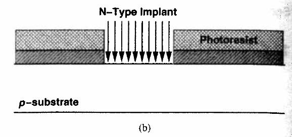
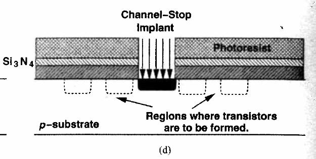
5 MOS Fabrication Sequence [Razavi] 5

6 MOS Fabrication Sequence [Razavi] 6
![MOS Fabrication Sequence [Razavi] Front-End](/docs-images/73/68814460/images/7-0.jpg "Back-End A silicide step, where highly")


7 MOS Fabrication Sequence [Razavi] Front-End Back-End A silicide step, where highly conductive metal is deposited on the gate and diffusion regions, reduces transistor terminal resistance To prevent potential gatesource/drain shorting an oxide spacer is first formed before silicide deposition 7

8 Contact and Metal Fabrication [Razavi] 8
9 Transistor Geometries -based design rules allow a process and feature sizeindependent way of setting mask dimensions to scale Due to complexity of modern processing, not used often today X L Minimum drawing feature = Assume w.c. mask alignment <0.75 Relative misalignment between masks is <1.5 AGate W * L AD, AS W * X PS, PS W X (3 sides) X depends on contact size 5 in this example 9
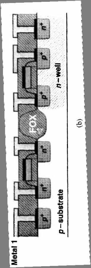
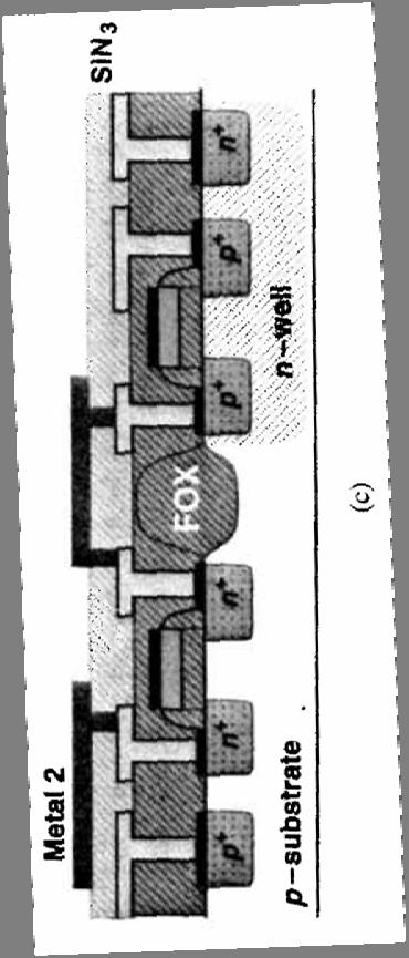
10 BASIC SCNA CMOS LAYERS Physical Layer N-well Silicon Nitride Polysilicon Layer 1 Polysilicon Layer P+ Ion Implant N+ Ion Implant Contact cut to n+/p_ Metal 1 Via Oxide Cuts Metal Pad Contact (Overglass) P-channel MOSFET CVD Oxide Drain Metal 1 Source Poly Gate p+ Gate Oxide n-well Bulk p+ p substrate Bulk N-channel MOSFET CVD Oxide Metal 1 Source Drain Poly Gate n+ Gate Oxide p substrate n+ 10 Bulk
11 X Design Rule Basics d S Minimum width and spacing Depletion regions (a) Mask definition n+ Nd X Implanted dopants p, Na (b) After annealing Patterning sequence for a doped n+ line. x p n+ Nd S p, Na X n+ x Metal n+ d (a) Contact size p, Na Metal n+ (b) Side view Geometry of a contact cut n+ n+ p, Na Depletion regions due to parallel n+ lines 11 (a) Masking Design (b) Registration tolerance Contact spacing rule
12 Nselect Active area border Active Poly gate s Nselect n+ p-substrate Active n+ p-substrate W Gate overhang in MOSFET layout Poly gate Poly gate (a) Correct mask sizing (b) Incorrect mask sizing Formation of n+ regions in an n-channel MOSFET Active area border (a) No overhang (b) With misalignment Effect of misalignment without overhang Resist Poly gate s poly Metal Metal Metal W substrate substrate substrate Gate spacing form an n+ edge (a) Resist pattern (b) Isotropic etch (c) anisotropic etch Effect of misalignment without overhang 1
13 Mask Number Mask Layer 1 NWELL ACTIVE Nselect Active Poly 3 POLY W' W 4 SELECT 5 POLY CONTACT 6 ACTIVE CONTACT 7 METAL1 8 VIA L' n+ n+ L FrontView Side View 9 METAL 10 PAD 11 POLY Difference between the drawn and physical values for channel length and the channel width Design Rule Layers 13
14 Polysilicon Gate n+ Gate Oxide p substrate (Bulk) Bulk n+ Metal Drain Polysilicon Gate W Field oxide n+ L n+ p L' x ox Structure of a n-channel MOSFET Active contact n+/p+ n+/p+ Poly Example of Layout Rules or Poly contact 14 Perspective view of an n-channel MOSFET Minimum transistor width is set by minimum diffusion width or 3 (check with TA) Often, we use a use a slightly larger minimum that is equal to the contact height (4 in this example)
15 N-channel MOSFET ECEN CVD Oxide Metal 1 Source Poly Gate Drain P-channel MOSFET CVD Oxide Drain Metal 1 Source Poly Gate n+ n+ Gate Oxide p substrate p+ Gate Oxide p+ n-well Bulk p substrate Gate Bulk (a) Cross section Bulk Gate Source Drain Drain Source Bulk (b) Circuit symbol Bulk n+ Poly n+ W L (c) Top 15 view
16 Stick Diagrams Poly Metal 1 G D N+/P+ Contact S (a) Definitions (b) MOSFET V DD V DD V DD M p M p M p In V in V out In Out Out M n M n Gnd M n Gnd Stick diagrams for the CMOS Inverter 16
17 The CMOS Inverter V DD V DD V DD M p M p M p In V in V out In Out Out M n M n Gnd M n Gnd W p N-Well n+ Metal VDD Lp Metal V DD p+ pfet nfet Metal GND p+ L N L p Metal Out pfet Poly In nfet W N W p n+ W N Basic Inverter Layout 17 L N Alternate Inverter Layout
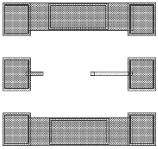
18 Standard Cells: VDD, VSS and output run in Parallel Metal V DD pfet B MpB MpA Vo MnB Out CMOS NAND logic gate A MnA A n+ B nfet Metal GND Metal V DD MpA pfet p+ MpB A B Vo nfet Out MnA MnB CMOS NOR logic gate A B Metal GND 18
19 Wide Analog Transistor: Analog techniques Unacceptable drain and source resistance Stray resistances in transistor structure Contacts short the distributed resistance of diffused areas Most of the current will be shrunk to this side Current is spread 19
20 Transistor orientation Orientation is important in analog circuits for matching purposes 0
21 Stacked Transistors Wide transistors need to be split Parallel connection of n elements (n = 4 for this example) Contact space is shared among transistors Parasitic capacitances are reduced (important for high speed ) Gate resistance is reduced Drain Gate Source Note that parasitic capacitors are lesser at the drain 1
22 Matched Transistors Simple layouts are prone to process variations, e.g. V T, KP, C ox Matched transistors require elaborated layout techniques M1 M Process Variations Drain M1 Differential pair requiring matched transistors Drain M Source

23 Interdigitized Layout Averages the process variations among transistors Common terminal is like a serpentine 3
24 Why Interdigitized? M1 M M M1 M1 M M M1 KP=1 KP KP3 KP4 KP5 KP6 KP7 KP8 Process variations are averaged among transistors KPs for M1:KP1+KP4+KP5+KP8 (Avg=4.5) M:KP+KP3+KP6+KP7 (Avg=4.5) Technique maybe good for matching dc conditions Uneven total drain area between M1 and M. This is undesirable for ac conditions: capacitors and other parameters may not be equal A more robust approach is needed (Use dummies if needed!!) 4

25 A method of achieving better capacitive matching : Using the previous slide values, we would have M with KP=3.5 and M1 with KP=5.5 Each transistor is split in four equal parts interleaved in two by two s. So that for one pair of pieces of the same transistor we have currents flowing in opposite direction. Transistors have the same source and drain area and perimeters, but this topology is more susceptible to gradients 5 (not common centroid)
26 Common Centroid Layouts Usually routing is more complex M1 M M1 M M M1 M M1 M1 M M1 M M M1 M M CENTROID (complex layout) M1: 8 transistors (0,3) (0,1) (1,) (1,0) (,3) (,1) (3,) (3,0) M: 8 transistors (0,) (0,0) (1,3) (1,1 (,) (,0) (3,3) (3,1) 6
!")
27 Common Centroid Layouts Split into parallel connections of even parts Half of them will have the drain at the right side and half at the left Be careful how you route the common terminal Cross talk (effect of distributed capacitors RF applications)! 7


28 Many contacts placed close to one another reduces series resistance and make the surface of metal connection smoother than when we use only one contact; this prevents microcraks in metal; Splitting the transistor in a number of equal part connected in parallel reduces the area of each transistor and so reduces further the parasitic capacitances, but accuracy might be degraded! 8
29 Integrated Resistors Highly resistive layers (p +, n +, well or polysilicon) R defines the resistance of a square of the layer Accuracy less than 30% Current flow L t Resistivity (volumetric measure of material s resistive characteristic) (-cm) W Sheet resistance (measure of the resistance of a uniform film with arbitrary thickness t R = /t ( ) W L W L R = R contact + (L/W) R 9
30 Diffusion resistors Diffused resistance p-substrate Diffused resistance well resistance Pinched n-well resistance 30
31 Poly Resistors First polysilicon resistance First polysilicon resistance with a well shielding Second polysilicon resistance Second polysilicon resistance with a well shielding 31
32 TYPICAL INTEGRATED RESISTORS R R cont L W R L W Type of layer n + diff Sheet Resistance W/ Accuracy % 0-40 Temperature Coefficient ppm/ o C 00-1K Voltage Coefficient ppm/v p + diff K n - well K - 4K K 10K p - well 3K - 6K K 10K pinched n - well 6K - 10K K pinched p - well 9K - 13K K first poly second poly Special poly sheet resistance for some analog processes might be as high as 1. K/ 3
33 Large Resistors In order to implement large resistors : Use long strips (large L/W) Use layers with high sheet resistance (bad performances see previous table) High temperature coefficient and non-linearityt Layout : rectangular serpentine R L W R L W x j Estimating the resistance in the corners can be difficult 33

34 Well-Diffusion Resistor Example shows two long resistors for K range Alternatively, serpentine shapes can be used Noise problems from the body Substrate bias surrounding the well Substrate bias between the parallel strips Dummies 34
35 Factors affecting accuracy : Plastic packages cause a large pressure on the die (= 800 Atm.). It determines a variation of the resistivity. For <100> material the variation is unisotropic, so the minimum is obtained if the resistance have a 45 o orientation. compensated Temperature : Temperature gradient on the chip may produce thermal induced mismatch. uncompensated 35
36 Etching Wet etching : isotropic (undercut effect) HF for SiO ; H 3 PO 4 for Al x for polysilicon may be m with standard deviation m. Reactive ion etching (R.I.E.)(plasma etching associated to bombardment ) : unisotropic. x for polysilicon is 0.05 m with standard deviation 0.01 m Boundary : The etching depends on the boundary conditions Use dummy strips 36


37 Side diffusion effect : Contribution of endings Side Diffusion widens R R is not constant with W Impact of R cont depends on relative geometry Best to always use a resistor W that is at least as large as the contact Interdigitized structure : 37
38 MOS Capacitors [Razavi] One of the most dense capacitors available (ff/um ) Often used to de-couple DC power supply and bias signals Capacitor non-linearity can be important if used in the signal path 38


")
39 Integrated Capacitors Poly -Diffusion Poly -Poly Metal1 -Poly [Razavi] Vertical Metal Sandwich Lateral Metal-Oxide-Metal (MOM) [Wang] [Ho] 39


40 Poly1 - Poly Capacitor Poly Poly 1 Area is determined by poly Problems undercut effects nonuniform dielectric thickness matching among capacitors 40
41 Factor affecting RELATIVE accuracy/matching Oxide damage Impurities Bias condition Bias history (for CVD) Stress Temperature Grow rate Poly grain size t t ox ox ox ox y y Real Area of Poly x x Etching Alignment L W ; L W C C 1 0.1% C C r r t t ox ox L L W W Note, the absolute C may vary as high as 0% due to process variations 41
42 Accuracy of integrated capacitors Perimeter imperfections effect the total capacitance: C = C A A A = (x-x)(y- y) = xy - xy - yx + 4x y Assuming that x = y = e A = xy - e(x + y) + 4(e) A xy - e(x + y) C e = - e(x + y) The relative error is = C e /C = -e(x + y) / xy C A = capacitance per unit area y y Real Area of Poly x x Then maximize the area and minimize the perimeter use squares!!! 4
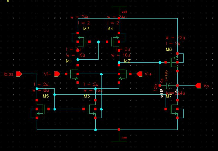
43 Capacitor Matching If we want to match the ratio of two caps C 1 and C C C 1 C C 1, ideal, ideal 1 e 1 e To minimize the error in the cap ratio, we need to have e 1 =e. This implies that the Perimeter/Area should be equal. Generally, we break up both caps C 1 and C into square unit caps, C u 1 Au x u 43
44 Capacitor Matching If both C 1 and C are integer multiples of C u, then simply use I 1 unit caps for C 1 and I unit caps for C Perimeter as a unit cap. Area Why is the non - unit cap Because we don' t want a than C. but none smaller than. 1 C C 1 If C1 I1Cu and C ICu 1 then we want the non - unit cap, C u I I 1 C C Overall, we want to use as C u f C u f nu? u u C u, 1 where f cap smaller than the unit cap, or bigger C u many unit caps as f, is a fraction, to have equal possible, 44
45 Capacitor Matching How to size C nu? Define N 1 f For matching P P x nu u nu From N definition Nx Nx 0 Plugging this into the previous expression, we can solve for y y nu nu A A y x nu u nu u u y nu If you want y P A N nu nu nu u N N Nx x A A u nu nu u P A N u u xnu y 4x x u nu x nu nu xu nu y u Nx y nu choose " ", y nu x nu choose "-" y nu 45
46 Capacitor Matching 46 u u u nu u nu nu u nu nu u nu u u u u C I C C N N N x y N N N x y y x N x y x N x f N f N C f C I C C f C I C to set generally we have the flexibility to size Although, 1 and 1 where 1 and 1 If 1
")
47 Common Centroid Capacitor Layout Unit capacitors are connected in parallel to form a larger capacitance Typically the ratio among capacitors is what matters The error in one capacitor is proportional to perimeter-area ratio Use dummies for better matching (See Razavi Book, page 75) 47
48 Approximate Common Centroid Structure C 1 C C 3 C 4 C 5 TC 1 TC TC 3 TC 4 TC 5 C = C 1 C 3 = C 1 C 4 = 4C 1 C 5 = 8C 1 48
49 Floating Capacitors Be aware of parasitic capacitors Polysilicon-Polysilicon: Bottom plate capacitance is comparable (10-30 %) with the poly-poly capacitance poly C P1 poly1 C P C P C 1 C P1 C1 C P substrate CP1, CP are very small (1-5 % of C1) CP is around % of C1 Metal1-Metal: More clean, but the capacitance per micrometer square is smaller. Good option for very high frequency applications ( C~ pf). C P1 metal metal1 C 1 C P Thick oxide substrate CP is very small (1-5 % of C1) 49
50 Analog Cell Layout Key Points Use transistors with the same orientation Minimize S/D contact area by stacking transistors (to reduce parasitic capacitance to substrate) Respect symmetries Use low resistive paths when current needs to be carried (to avoid parasitic voltage drops) Shield critical nodes (to avoid undesired noise injection) Include guard rings everywhere; e.g. Substrate/well should not have regions larger than 50 um without guard protections (latchup issues) 50
![Bipolar Transistors Latchup [Razavi] Equivalent Circuit Potential for parasitic BJTs (Vertical PNP and Lateral NPN) to form a positive feedback loop circuit If circuit is triggered, due to](/docs-images/73/68814460/images/51-0.jpg "current injected into substrate, then a large current can be drawn through the circuit and cause damage Important to minimize substrate and well resistance with many contacts/guard rings")
51 Bipolar Transistors Latchup [Razavi] Equivalent Circuit Potential for parasitic BJTs (Vertical PNP and Lateral NPN) to form a positive feedback loop circuit If circuit is triggered, due to current injected into substrate, then a large current can be drawn through the circuit and cause damage Important to minimize substrate and well resistance with many contacts/guard rings 51
52 Stacked Layout for Analog Cells Stack of elements with the same width Transistors with even number of parts have the source (drain) on both sides of the stack Transistors with odd number of parts have the source on one end and the drain on the other. If matching is critical use dummies If different transistors share a same node they can be combined in the same stack to share the area of the same node (less parasitics) Use superimposed or side by side stacks to integrate the cell 5
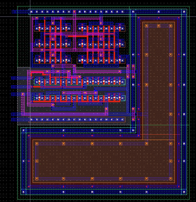
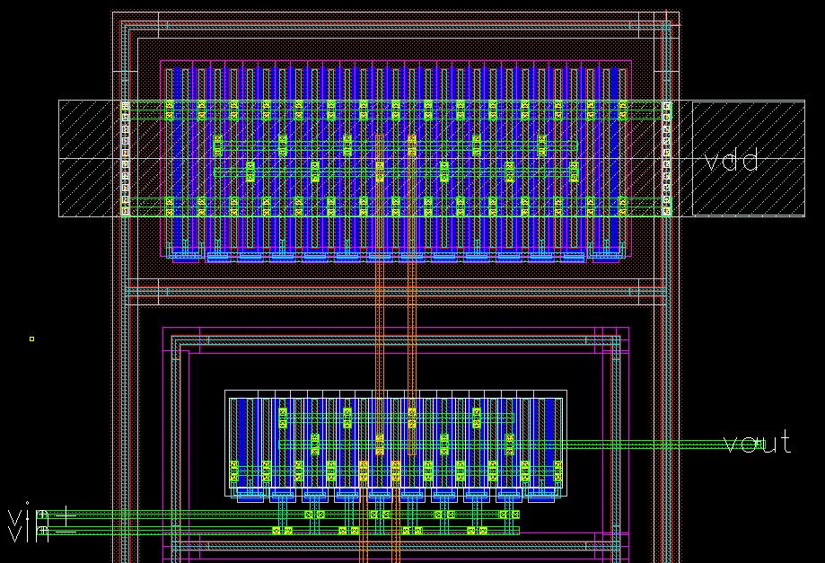
53 M1 and M must match. Layout is interdigitized M3 and M4 must match. M6 must be wider by 4*M3 M7 must be *M5 Layout is an interconnection of 3 stacks; for NMOS and 1 for PMOS Capacitor made by poly-poly Not the best floorplan, but OK M3 M4 M3 M6 M6 M6 M6 M4 M1 M M6 M1 M M1 M M1 M C M5 M8 M7 M5 M7 M7 M7 M7 M5 M8 Pay attention to your floor plan! It is critical for minimizing iterations: Identify the critical elements 53
54 54
55 55
56 Following slides were provided by some of Dr. Silva s graduate students. Special thanks to Fabian Silva-Rivas, Venkata Gadde, Marvin Onabajo, Cho-Ying Lu, Raghavendra Kulkarni and Jusung Kim 56
 3. Resistors for V CM 4.Capacitors (Common centroid)")
57 4 1 3 Figure: Layout of a single stage fully differential amplifier and its CMFB circuit I/p NMOS diff pair. PMOS (Interdigitated) 3. Resistors for V CM 4.Capacitors (Common centroid)

58 Resistive network Capacitive network (Common centroid) Fully differential amplifier Figure: Layout of a second order Active 58 RC low-pass Filter (Bi-quad)

59 3-bit quantizer in Jazz 0.18μm CMOS technology S/H: sample-and-hold circuit that is used to sample the continuous-input signal Core: contains matched differential pairs and resistors to create accurate reference levels for the analog-todigital conversion Latches: store the output bits; provide interface to digital circuitry with rail-to-rail voltage levels 59
 clocked at 400MHz The sensitive")
60 High-speed D-Flip-Flop in Jazz 0.18μm CMOS technology Resolves a small differential input with 10mV < V p-p < 150mV in less than 360ps Provides digital output (differential, rail-to-rail) clocked at 400MHz The sensitive input stage (1 st differential pair) has a 60separate analog supply line to isolate it from the noise on the supply line caused by switching of digital circuitry
:")
61 Design example (industrial quality): Simplest OTA 61

62 Overall amplifier: Have a look on the guard rings and additional well! 6

63 BIAS: you may be able to see the dummies, symmetry and S/D connections 63

64 From downstairs Differential pair 64
65 65

66 Details on the P-type current mirrors 66
67 Q-value of Spiral Inductors in CMOS Process Most of the following slides were taken from Seminar by: Park, Sang Wook TAMU,


68 What is Q? energy stored Q average power dissipated Simple Inductor Model: Q L R s s Integrated Spiral Inductor Pi Model 68
69 De-Embedding 69
70 Equivalent Circuit & Calculation Cs Port1 Ls Rs Port 9 8 Q-factor 7 Cox1 Cox Csub Rsub Csub Rsub Frequncy (GHz) Equivalent Circuit Parameter Calculation 70
 W : Width (=14.")
71 Layout & Structure Metal-6 (thickness=um) N : # of Turns Metal-5 under path Via-5 R : Radius Oxide Substrate S : Space (=1.5um) W : Width (=14.5um) 71

 octagon (R=60) square (R=30)")
 Shape : Octagon > Square")
72 9 8 7 Shape & Radius Layout Split 1 Q-factor NxWxS (4.5x15x1.5) square (R=60) octagon (R=60) 3 1 square (R=60) octagon (R=60) square (R=30) octagon (R=30) square (R=30) Frequncy (GHz) Shape : Octagon > Square Radius : 60 > 30 7 octagon (R=30)
 material none nwell poly metal1 Q-factor")
 0 1 3 4 5 6 Frequncy (GHz) none nwell poly metal 1")
73 Layout Split PGS (Patterned Ground Shield) material none nwell poly metal1 Q-factor NxRxWxS (4.5x60x15x1.5) Frequncy (GHz) none nwell poly metal 1 PGS : Poly > Nwell > none > Metal1 73
 none poly PGS(wide) SGS poly 3 1 none poly PGS(wide) nonsal poly SGS nonsal poly PGS poly PGS 0 0 1 3 4 5 6 Frequncy (GHz) GS : Poly PGS > Poly(nonsal) SGS > Poly(nonsal)")
74 Layout Split 3 GS (Ground Shield) type Q-factor NxRxWxS (4.5x60x15x1.5) none poly PGS(wide) SGS poly 3 1 none poly PGS(wide) nonsal poly SGS nonsal poly PGS poly PGS Frequncy (GHz) GS : Poly PGS > Poly(nonsal) SGS > Poly(nonsal) PGS > none PGS = patterned ground shield SGS = solid ground shield 74 nonsal poly SGS poly PGS
 M 6 M 5/6 M 4/5/6 0 0 1 3 4 5 6 Frequncy (GHz) M 3/4/5/6 Stack : M6 > M5/6 > M4/5/6 > M3/4/5/6 75")
75 M 6 M 5/6 M 4/5/6 M 3/4/5/6 Metal Stack Layout Split 4 Q-factor NxRxWxS (4.5x60x15x1.5) M 6 M 5/6 M 4/5/ Frequncy (GHz) M 3/4/5/6 Stack : M6 > M5/6 > M4/5/6 > M3/4/5/6 75

76 TAMU Mixed-Signal Research Chip A 10 Gb/s Hybrid ADC-Based Receiver w/ Embedded Analog and Per-Symbol Dynamically Enabled Digital Equalization 10GS/s asynchronous SAR ADC with embedded 3-tap FFE Digital equalizer with 4-tap FFE and 3-tap DFE Fabricated in GP 65nm CMOS BER w/ 36.4dB Loss Channel A. Shafik et al, A 10Gb/s Hybrid ADC-Based Receiver with Embedded 3-Tap Analog FFE and Dynamically-Enabled Digital Equalization in 65nm CMOS, ISSCC 015. A. Shafik et al, A 10 Gb/s Hybrid ADC-Based Receiver With Embedded Analog and Per-Symbol Dynamically Enabled Digital Equalization, JSSC
77 Next Time Table-Based (g m /I D ) Design Examples 77
ECEN474: (Analog) VLSI Circuit Design Fall 2012
 VLSI Circuit Design Fall 2012") ECEN474: (Analog) VLSI Circuit Design Fall 2012 Lecture 5: Layout Techniques Sam Palermo Analog & Mixed-Signal Center Texas A&M University Announcements HW1 due today at 5PM For grad students, confirm
ECEN474: (Analog) VLSI Circuit Design Fall 2012 Lecture 5: Layout Techniques Sam Palermo Analog & Mixed-Signal Center Texas A&M University Announcements HW1 due today at 5PM For grad students, confirm
ECEN474: (Analog) VLSI Circuit Design Fall 2010
 VLSI Circuit Design Fall 2010") ECEN474: (Analog) VLSI Circuit Design Fall 2010 Lecture 6: Layout Techniques Sam Palermo Analog & Mixed-Signal Center Texas A&M University Announcements Lab 2 next week Has a prelab Upgrading Cadence version
ECEN474: (Analog) VLSI Circuit Design Fall 2010 Lecture 6: Layout Techniques Sam Palermo Analog & Mixed-Signal Center Texas A&M University Announcements Lab 2 next week Has a prelab Upgrading Cadence version
Fundamentals of ANALOG TO DIGITAL CONVERTERS: Part I.3. Technology
 Fundamentals of ANALOG TO DIGITAL CONVERTERS: Part I.3 Technology January 019 Texas A&M University 1 Spring, 019 Well-Diffusion Resistor Example shows two long resistors for K range Alternatively, serpentine
CMOS Cross Section. EECS240 Spring Dimensions. Today s Lecture. Why Talk About Passives? EE240 Process
 EECS240 Spring 202 CMOS Cross Section Metal p - substrate p + diffusion Lecture 2: CMOS Technology and Passive Devices Poly n - well n + diffusion Elad Alon Dept. of EECS EECS240 Lecture 2 4 Today s Lecture
EECS240 Spring Today s Lecture. Lecture 2: CMOS Technology and Passive Devices. Lingkai Kong EECS. EE240 CMOS Technology
 EECS240 Spring 2013 Lecture 2: CMOS Technology and Passive Devices Lingkai Kong EECS Today s Lecture EE240 CMOS Technology Passive devices Motivation Resistors Capacitors (Inductors) Next time: MOS transistor
LAYOUT TECHNIQUES. Dr. Ivan Grech
 LAYOUT TECHNIQUES OUTLINE Transistor Layout Resistor Layout Capacitor Layout Floor planning Mixed A/D Layout Automatic Analog Layout Layout Techniques Main Layers in a typical Double-Poly, Double-Metal
CMOS Cross Section. EECS240 Spring Today s Lecture. Dimensions. CMOS Process. Devices. Lecture 2: CMOS Technology and Passive Devices
 EECS240 Spring 2008 CMOS Cross Section Metal p - substrate p + diffusion Lecture 2: CMOS echnology and Passive Devices Poly n - well n + diffusion Elad Alon Dept. of EECS EECS240 Lecture 2 4 oday s Lecture
Lecture 4: CMOS Transistor Theory
 Introduction to CMOS VLSI Design Lecture 4: CMOS Transistor Theory David Harris, Harvey Mudd College Kartik Mohanram and Steven Levitan University of Pittsburgh Outline q Introduction q MOS Capacitor q
ELEN0037 Microelectronic IC Design. Prof. Dr. Michael Kraft
 ELEN0037 Microelectronic IC Design Prof. Dr. Michael Kraft Lecture 2: Technological Aspects Technology Passive components Active components CMOS Process Basic Layout Scaling CMOS Technology Integrated
VLSI VLSI CIRCUIT DESIGN PROCESSES P.VIDYA SAGAR ( ASSOCIATE PROFESSOR) Department of Electronics and Communication Engineering, VBIT
 Department of Electronics and Communication Engineering, VBIT") VLSI VLSI CIRCUIT DESIGN PROCESSES P.VIDYA SAGAR ( ASSOCIATE PROFESSOR) SYLLABUS UNIT II VLSI CIRCUIT DESIGN PROCESSES: VLSI Design Flow, MOS Layers, Stick Diagrams, Design Rules and Layout, 2 m CMOS Design
VLSI VLSI CIRCUIT DESIGN PROCESSES P.VIDYA SAGAR ( ASSOCIATE PROFESSOR) SYLLABUS UNIT II VLSI CIRCUIT DESIGN PROCESSES: VLSI Design Flow, MOS Layers, Stick Diagrams, Design Rules and Layout, 2 m CMOS Design
CMOS Devices. PN junctions and diodes NMOS and PMOS transistors Resistors Capacitors Inductors Bipolar transistors
 CMOS Devices PN junctions and diodes NMOS and PMOS transistors Resistors Capacitors Inductors Bipolar transistors PN Junctions Diffusion causes depletion region D.R. is insulator and establishes barrier
Lecture 0: Introduction
 Lecture 0: Introduction Introduction q Integrated circuits: many transistors on one chip q Very Large Scale Integration (VLSI): bucketloads! q Complementary Metal Oxide Semiconductor Fast, cheap, low power
EE382M-14 CMOS Analog Integrated Circuit Design
 EE382M-14 CMOS Analog Integrated Circuit Design Lecture 3, MOS Capacitances, Passive Components, and Layout of Analog Integrated Circuits MOS Capacitances Type of MOS transistor capacitors Depletion capacitance
VLSI GATE LEVEL DESIGN UNIT - III P.VIDYA SAGAR ( ASSOCIATE PROFESSOR) Department of Electronics and Communication Engineering, VBIT
 Department of Electronics and Communication Engineering, VBIT") VLSI UNIT - III GATE LEVEL DESIGN P.VIDYA SAGAR ( ASSOCIATE PROFESSOR) contents GATE LEVEL DESIGN : Logic Gates and Other complex gates, Switch logic, Alternate gate circuits, Time Delays, Driving large
VLSI UNIT - III GATE LEVEL DESIGN P.VIDYA SAGAR ( ASSOCIATE PROFESSOR) contents GATE LEVEL DESIGN : Logic Gates and Other complex gates, Switch logic, Alternate gate circuits, Time Delays, Driving large
MOS Transistor Properties Review
 MOS Transistor Properties Review 1 VLSI Chip Manufacturing Process Photolithography: transfer of mask patterns to the chip Diffusion or ion implantation: selective doping of Si substrate Oxidation: SiO
MOS Transistor I-V Characteristics and Parasitics
 ECEN454 Digital Integrated Circuit Design MOS Transistor I-V Characteristics and Parasitics ECEN 454 Facts about Transistors So far, we have treated transistors as ideal switches An ON transistor passes
ECEN 474/704 Lab 2: Layout Design
 ECEN 474/704 Lab 2: Layout esign Objectives Learn Techniques for successful integrated circuit layout design. Introduction In this lab you will learn in detail how to generate a simple transistor layout.
Digital Integrated Circuits A Design Perspective
 Semiconductor Memories Adapted from Chapter 12 of Digital Integrated Circuits A Design Perspective Jan M. Rabaey et al. Copyright 2003 Prentice Hall/Pearson Outline Memory Classification Memory Architectures
Topics to be Covered. capacitance inductance transmission lines
 Topics to be Covered Circuit Elements Switching Characteristics Power Dissipation Conductor Sizes Charge Sharing Design Margins Yield resistance capacitance inductance transmission lines Resistance of
Microelectronics Part 1: Main CMOS circuits design rules
 GBM8320 Dispositifs Médicaux telligents Microelectronics Part 1: Main CMOS circuits design rules Mohamad Sawan et al. Laboratoire de neurotechnologies Polystim! http://www.cours.polymtl.ca/gbm8320/! med-amine.miled@polymtl.ca!
MOS Transistor Theory
 MOS Transistor Theory So far, we have viewed a MOS transistor as an ideal switch (digital operation) Reality: less than ideal EE 261 Krish Chakrabarty 1 Introduction So far, we have treated transistors
Device Models (PN Diode, MOSFET )
") Device Models (PN Diode, MOSFET ) Instructor: Steven P. Levitan steve@ece.pitt.edu TA: Gayatri Mehta, José Martínez Book: Digital Integrated Circuits: A Design Perspective; Jan Rabaey Lab Notes: Handed
Device Models (PN Diode, MOSFET ) Instructor: Steven P. Levitan steve@ece.pitt.edu TA: Gayatri Mehta, José Martínez Book: Digital Integrated Circuits: A Design Perspective; Jan Rabaey Lab Notes: Handed
Circuits. L5: Fabrication and Layout -2 ( ) B. Mazhari Dept. of EE, IIT Kanpur. B. Mazhari, IITK. G-Number
 B. Mazhari Dept. of EE, IIT Kanpur. B. Mazhari, IITK. G-Number") EE610: CMOS Analog Circuits L5: Fabrication and Layout -2 (12.8.2013) B. Mazhari Dept. of EE, IIT Kanpur 44 Passive Components: Resistor Besides MOS transistors, sometimes one requires to implement passive
EE610: CMOS Analog Circuits L5: Fabrication and Layout -2 (12.8.2013) B. Mazhari Dept. of EE, IIT Kanpur 44 Passive Components: Resistor Besides MOS transistors, sometimes one requires to implement passive
Section 12: Intro to Devices
 Section 12: Intro to Devices Extensive reading materials on reserve, including Robert F. Pierret, Semiconductor Device Fundamentals EE143 Ali Javey Bond Model of Electrons and Holes Si Si Si Si Si Si Si
MOSFET: Introduction
 E&CE 437 Integrated VLSI Systems MOS Transistor 1 of 30 MOSFET: Introduction Metal oxide semiconductor field effect transistor (MOSFET) or MOS is widely used for implementing digital designs Its major
ECE 497 JS Lecture - 12 Device Technologies
 ECE 497 JS Lecture - 12 Device Technologies Spring 2004 Jose E. Schutt-Aine Electrical & Computer Engineering University of Illinois jose@emlab.uiuc.edu 1 NMOS Transistor 2 ρ Source channel charge density
Lecture 3: CMOS Transistor Theory
 Lecture 3: CMOS Transistor Theory Outline Introduction MOS Capacitor nmos I-V Characteristics pmos I-V Characteristics Gate and Diffusion Capacitance 2 Introduction So far, we have treated transistors
ECE 342 Electronic Circuits. Lecture 6 MOS Transistors
 ECE 342 Electronic Circuits Lecture 6 MOS Transistors Jose E. Schutt-Aine Electrical & Computer Engineering University of Illinois jesa@illinois.edu 1 NMOS Transistor Typically L = 0.1 to 3 m, W = 0.2
EEC 118 Lecture #2: MOSFET Structure and Basic Operation. Rajeevan Amirtharajah University of California, Davis Jeff Parkhurst Intel Corporation
 EEC 118 Lecture #2: MOSFET Structure and Basic Operation Rajeevan Amirtharajah University of California, Davis Jeff Parkhurst Intel Corporation Announcements Lab 1 this week, report due next week Bring
ESE 570: Digital Integrated Circuits and VLSI Fundamentals
 ESE 570: Digital Integrated Circuits and VLSI Fundamentals Lec 4: January 23, 2018 MOS Transistor Theory, MOS Model Penn ESE 570 Spring 2018 Khanna Lecture Outline! CMOS Process Enhancements! Semiconductor
P. R. Nelson 1 ECE418 - VLSI. Midterm Exam. Solutions
 P. R. Nelson 1 ECE418 - VLSI Midterm Exam Solutions 1. (8 points) Draw the cross-section view for A-A. The cross-section view is as shown below.. ( points) Can you tell which of the metal1 regions is the
Introduction and Background
 Analog CMOS Integrated Circuit Design Introduction and Background Dr. Jawdat Abu-Taha Department of Electrical and Computer Engineering Islamic University of Gaza jtaha@iugaza.edu.ps 1 Marking Assignments
ECE 342 Electronic Circuits. 3. MOS Transistors
 ECE 342 Electronic Circuits 3. MOS Transistors Jose E. Schutt-Aine Electrical & Computer Engineering University of Illinois jschutt@emlab.uiuc.edu 1 NMOS Transistor Typically L = 0.1 to 3 m, W = 0.2 to
Lecture 12: MOSFET Devices
 Lecture 12: MOSFET Devices Gu-Yeon Wei Division of Engineering and Applied Sciences Harvard University guyeon@eecs.harvard.edu Wei 1 Overview Reading S&S: Chapter 5.1~5.4 Supplemental Reading Background
ESE 570: Digital Integrated Circuits and VLSI Fundamentals
 ESE 570: Digital Integrated Circuits and VLSI Fundamentals Lec 4: January 29, 2019 MOS Transistor Theory, MOS Model Penn ESE 570 Spring 2019 Khanna Lecture Outline! CMOS Process Enhancements! Semiconductor
Device Models (PN Diode, MOSFET )
") Device Models (PN Diode, MOSFET ) Instructor: Steven P. Levitan steve@ece.pitt.edu TA: Gayatri Mehta, José Martínez Book: Digital Integrated Circuits: A Design Perspective; Jan Rabaey Lab Notes: Handed
Device Models (PN Diode, MOSFET ) Instructor: Steven P. Levitan steve@ece.pitt.edu TA: Gayatri Mehta, José Martínez Book: Digital Integrated Circuits: A Design Perspective; Jan Rabaey Lab Notes: Handed
Lecture 040 Integrated Circuit Technology - II (5/11/03) Page ECE Frequency Synthesizers P.E. Allen
 Page ECE Frequency Synthesizers P.E. Allen") Lecture 040 Integrated Circuit Technology - II (5/11/03) Page 040-1 LECTURE 040 INTEGRATED CIRCUIT TECHNOLOGY - II (Reference [7,8]) Objective The objective of this presentation is: 1.) Illustrate and
Lecture 040 Integrated Circuit Technology - II (5/11/03) Page 040-1 LECTURE 040 INTEGRATED CIRCUIT TECHNOLOGY - II (Reference [7,8]) Objective The objective of this presentation is: 1.) Illustrate and
ECEN474/704: (Analog) VLSI Circuit Design Spring 2018
 VLSI Circuit Design Spring 2018") ECEN474/704: (Analog) SI Circuit Design Spring 2018 ecture 2: MOS ransistor Modeling Sam Palermo Analog & Mixed-Signal Center exas A&M University Announcements If you haven t already, turn in your 0.18um
ECEN474/704: (Analog) SI Circuit Design Spring 2018 ecture 2: MOS ransistor Modeling Sam Palermo Analog & Mixed-Signal Center exas A&M University Announcements If you haven t already, turn in your 0.18um
EECS 312: Digital Integrated Circuits Midterm Exam 2 December 2010
 Signature: EECS 312: Digital Integrated Circuits Midterm Exam 2 December 2010 obert Dick Show your work. Derivations are required for credit; end results are insufficient. Closed book. No electronic mental
EE115C Winter 2017 Digital Electronic Circuits. Lecture 3: MOS RC Model, CMOS Manufacturing
 EE115C Winter 2017 Digital Electronic Circuits Lecture 3: MOS RC Model, CMOS Manufacturing Agenda MOS Transistor: RC Model (pp. 104-113) S R on D CMOS Manufacturing Process (pp. 36-46) S S C GS G G C GD
ENEE 359a Digital VLSI Design
 SLIDE 1 ENEE 359a Digital VLSI Design & Logical Effort Prof. blj@ece.umd.edu Credit where credit is due: Slides contain original artwork ( Jacob 2004) as well as material taken liberally from Irwin & Vijay
Lecture 150 Basic IC Processes (10/10/01) Page ECE Analog Integrated Circuits and Systems P.E. Allen
 Page ECE Analog Integrated Circuits and Systems P.E. Allen") Lecture 150 Basic IC Processes (10/10/01) Page 1501 LECTURE 150 BASIC IC PROCESSES (READING: TextSec. 2.2) INTRODUCTION Objective The objective of this presentation is: 1.) Introduce the fabrication of
Lecture 150 Basic IC Processes (10/10/01) Page 1501 LECTURE 150 BASIC IC PROCESSES (READING: TextSec. 2.2) INTRODUCTION Objective The objective of this presentation is: 1.) Introduce the fabrication of
Semiconductor Memories
 Semiconductor References: Adapted from: Digital Integrated Circuits: A Design Perspective, J. Rabaey UCB Principles of CMOS VLSI Design: A Systems Perspective, 2nd Ed., N. H. E. Weste and K. Eshraghian
Lecture 12: MOS Capacitors, transistors. Context
 Lecture 12: MOS Capacitors, transistors Context In the last lecture, we discussed PN diodes, and the depletion layer into semiconductor surfaces. Small signal models In this lecture, we will apply those
Semiconductor memories
 Semiconductor memories Semiconductor Memories Data in Write Memory cell Read Data out Some design issues : How many cells? Function? Power consuption? Access type? How fast are read/write operations? Semiconductor
Lecture 11: MOS Transistor
 Lecture 11: MOS Transistor Prof. Niknejad Lecture Outline Review: MOS Capacitors Regions MOS Capacitors (3.8 3.9) CV Curve Threshold Voltage MOS Transistors (4.1 4.3): Overview Cross-section and layout
Digital Integrated Circuits A Design Perspective. Semiconductor. Memories. Memories
 Digital Integrated Circuits A Design Perspective Semiconductor Chapter Overview Memory Classification Memory Architectures The Memory Core Periphery Reliability Case Studies Semiconductor Memory Classification
Lecture 020 Review of CMOS Technology (09/01/03) Page 020-1
 Page 020-1") Lecture 020 Review of CMOS Technology (09/01/03) Page 020-1 LECTURE 020 REVIEW OF CMOS TECHNOLOGY INTRODUCTION Objective Provide sufficient background to understand the limits and capabilities of CMOS
Lecture 020 Review of CMOS Technology (09/01/03) Page 020-1 LECTURE 020 REVIEW OF CMOS TECHNOLOGY INTRODUCTION Objective Provide sufficient background to understand the limits and capabilities of CMOS
Today s lecture. EE141- Spring 2003 Lecture 4. Design Rules CMOS Inverter MOS Transistor Model
 - Spring 003 Lecture 4 Design Rules CMOS Inverter MOS Transistor Model Today s lecture Design Rules The CMOS inverter at a glance An MOS transistor model for manual analysis Important! Labs start next
! CMOS Process Enhancements. ! Semiconductor Physics. " Band gaps. " Field Effects. ! MOS Physics. " Cut-off. " Depletion.
 ESE 570: Digital Integrated Circuits and VLSI Fundamentals Lec 4: January 3, 018 MOS Transistor Theory, MOS Model Lecture Outline! CMOS Process Enhancements! Semiconductor Physics " Band gaps " Field Effects!
! CMOS Process Enhancements. ! Semiconductor Physics. " Band gaps. " Field Effects. ! MOS Physics. " Cut-off. " Depletion.
 ESE 570: Digital Integrated Circuits and VLSI Fundamentals Lec 4: January 9, 019 MOS Transistor Theory, MOS Model Lecture Outline CMOS Process Enhancements Semiconductor Physics Band gaps Field Effects
UNIVERSITY OF CALIFORNIA College of Engineering Department of Electrical Engineering and Computer Sciences. Professor Oldham Fall 1999
 UNIVERSITY OF CLIFORNI College of Engineering Department of Electrical Engineering and Computer Sciences Professor Oldham Fall 1999 EECS 40 FINL EXM 13 December 1999 Name: Last, First Student ID: T: Kusuma
The Devices. Jan M. Rabaey
 The Devices Jan M. Rabaey Goal of this chapter Present intuitive understanding of device operation Introduction of basic device equations Introduction of models for manual analysis Introduction of models
EE 230 Lecture 31. THE MOS TRANSISTOR Model Simplifcations THE Bipolar Junction TRANSISTOR
 EE 23 Lecture 3 THE MOS TRANSISTOR Model Simplifcations THE Bipolar Junction TRANSISTOR Quiz 3 Determine I X. Assume W=u, L=2u, V T =V, uc OX = - 4 A/V 2, λ= And the number is? 3 8 5 2? 6 4 9 7 Quiz 3
CMPEN 411 VLSI Digital Circuits. Lecture 03: MOS Transistor
 CMPEN 411 VLSI Digital Circuits Lecture 03: MOS Transistor Kyusun Choi [Adapted from Rabaey s Digital Integrated Circuits, Second Edition, 2003 J. Rabaey, A. Chandrakasan, B. Nikolic] CMPEN 411 L03 S.1
Interconnects. Wire Resistance Wire Capacitance Wire RC Delay Crosstalk Wire Engineering Repeaters. ECE 261 James Morizio 1
 Interconnects Wire Resistance Wire Capacitance Wire RC Delay Crosstalk Wire Engineering Repeaters ECE 261 James Morizio 1 Introduction Chips are mostly made of wires called interconnect In stick diagram,
ECE 546 Lecture 10 MOS Transistors
 ECE 546 Lecture 10 MOS Transistors Spring 2018 Jose E. Schutt-Aine Electrical & Computer Engineering University of Illinois jesa@illinois.edu NMOS Transistor NMOS Transistor N-Channel MOSFET Built on p-type
ENEE 359a Digital VLSI Design
 SLIDE 1 ENEE 359a Digital VLSI Design Prof. blj@eng.umd.edu Credit where credit is due: Slides contain original artwork ( Jacob 2004) as well as material taken liberally from Irwin & Vijay s CSE477 slides
Characteristics of Passive IC Devices
 008/Oct 8 esistors Characteristics of Passive IC Devices Poly esistance Diffusion esistance Well esistance Parasitic esistance Capacitors Poly Capacitors MOS Capacitors MIM Capacitors Parasitic Capacitors
Chapter 4 Field-Effect Transistors
 Chapter 4 Field-Effect Transistors Microelectronic Circuit Design Richard C. Jaeger Travis N. Blalock 5/5/11 Chap 4-1 Chapter Goals Describe operation of MOSFETs. Define FET characteristics in operation
Lecture 7 Circuit Delay, Area and Power
 Lecture 7 Circuit Delay, Area and Power lecture notes from S. Mitra Intro VLSI System course (EE271) Introduction to VLSI Systems 1 Circuits and Delay Introduction to VLSI Systems 2 Power, Delay and Area:
The Inverter. Digital Integrated Circuits A Design Perspective. Jan M. Rabaey Anantha Chandrakasan Borivoje Nikolic
 Digital Integrated Circuits A Design Perspective Jan M. Rabaey Anantha Chandrakasan Borivoje Nikolic The Inverter Revised from Digital Integrated Circuits, Jan M. Rabaey el, 2003 Propagation Delay CMOS
Digital Integrated Circuits (83-313) Lecture 5: Interconnect. Semester B, Lecturer: Adam Teman TAs: Itamar Levi, Robert Giterman 1
 Lecture 5: Interconnect. Semester B, Lecturer: Adam Teman TAs: Itamar Levi, Robert Giterman 1") Digital Integrated Circuits (83-313) Lecture 5: Interconnect Semester B, 2015-16 Lecturer: Adam Teman TAs: Itamar Levi, Robert Giterman 1 What will we learn today? 1 A First Glance at Interconnect 2 3
Digital Integrated Circuits (83-313) Lecture 5: Interconnect Semester B, 2015-16 Lecturer: Adam Teman TAs: Itamar Levi, Robert Giterman 1 What will we learn today? 1 A First Glance at Interconnect 2 3
Lecture 210 Physical Aspects of ICs (12/15/01) Page 210-1
 Page 210-1") Lecture 210 Physical Aspects of ICs (12/15/01) Page 210-1 LECTURE 210 PHYSICAL ASPECTS OF ICs (READING: Text-Sec. 2.5, 2.6, 2.8) INTRODUCTION Objective Illustrate the physical aspects of integrated circuits
Lecture 210 Physical Aspects of ICs (12/15/01) Page 210-1 LECTURE 210 PHYSICAL ASPECTS OF ICs (READING: Text-Sec. 2.5, 2.6, 2.8) INTRODUCTION Objective Illustrate the physical aspects of integrated circuits
ECE520 VLSI Design. Lecture 23: SRAM & DRAM Memories. Payman Zarkesh-Ha
 ECE520 VLSI Design Lecture 23: SRAM & DRAM Memories Payman Zarkesh-Ha Office: ECE Bldg. 230B Office hours: Wednesday 2:00-3:00PM or by appointment E-mail: pzarkesh@unm.edu Slide: 1 Review of Last Lecture
Introduction to CMOS VLSI. Chapter 2: CMOS Transistor Theory. Harris, 2004 Updated by Li Chen, Outline
 Introduction to MOS VLSI Design hapter : MOS Transistor Theory copyright@david Harris, 004 Updated by Li hen, 010 Outline Introduction MOS apacitor nmos IV haracteristics pmos IV haracteristics Gate and
Self-study problems and questions Processing and Device Technology, FFF110/FYSD13
 Self-study problems and questions Processing and Device Technology, FFF110/FYSD13 Version 2016_01 In addition to the problems discussed at the seminars and at the lectures, you can use this set of problems
Lecture 25. Semiconductor Memories. Issues in Memory
 Lecture 25 Semiconductor Memories Issues in Memory Memory Classification Memory Architectures TheMemoryCore Periphery 1 Semiconductor Memory Classification RWM NVRWM ROM Random Access Non-Random Access
Chapter 3 Basics Semiconductor Devices and Processing
 Chapter 3 Basics Semiconductor Devices and Processing Hong Xiao, Ph. D. www2.austin.cc.tx.us/hongxiao/book.htm Hong Xiao, Ph. D. www2.austin.cc.tx.us/hongxiao/book.htm 1 Objectives Identify at least two
Lecture 23: Negative Resistance Osc, Differential Osc, and VCOs
 EECS 142 Lecture 23: Negative Resistance Osc, Differential Osc, and VCOs Prof. Ali M. Niknejad University of California, Berkeley Copyright c 2005 by Ali M. Niknejad A. M. Niknejad University of California,
Extensive reading materials on reserve, including
 Section 12: Intro to Devices Extensive reading materials on reserve, including Robert F. Pierret, Semiconductor Device Fundamentals EE143 Ali Javey Bond Model of Electrons and Holes Si Si Si Si Si Si Si
3. Design a stick diagram for the PMOS logic shown below [16] Y = (A + B).C. 4. Design a layout diagram for the CMOS logic shown below [16]
![3. Design a stick diagram for the PMOS logic shown below [16] Y = (A + B).C. 4. Design a layout diagram for the CMOS logic shown below [16]](/thumbs/96/128765118.jpg "3. Design a stick diagram for the PMOS logic shown below [16] Y = (A + B).C. 4. Design a layout diagram for the CMOS logic shown below [16]") Code No: RR420203 Set No. 1 1. (a) Find g m and r ds for an n-channel transistor with V GS = 1.2V; V tn = 0.8V; W/L = 10; µncox = 92 µa/v 2 and V DS = Veff + 0.5V The out put impedance constant. λ = 95.3
Code No: RR420203 Set No. 1 1. (a) Find g m and r ds for an n-channel transistor with V GS = 1.2V; V tn = 0.8V; W/L = 10; µncox = 92 µa/v 2 and V DS = Veff + 0.5V The out put impedance constant. λ = 95.3
Introduction to CMOS VLSI Design Lecture 1: Introduction
 Introduction to CMOS VLSI Design Lecture 1: Introduction David Harris, Harvey Mudd College Kartik Mohanram and Steven Levitan University of Pittsburgh Introduction Integrated circuits: many transistors
Digital Integrated Circuits. The Wire * Fuyuzhuo. *Thanks for Dr.Guoyong.SHI for his slides contributed for the talk. Digital IC.
 Digital Integrated Circuits The Wire * Fuyuzhuo *Thanks for Dr.Guoyong.SHI for his slides contributed for the talk Introduction The Wire transmitters receivers schematics physical 2 Interconnect Impact
MOS Transistor Theory
 CHAPTER 3 MOS Transistor Theory Outline 2 1. Introduction 2. Ideal I-V Characteristics 3. Nonideal I-V Effects 4. C-V Characteristics 5. DC Transfer Characteristics 6. Switch-level RC Delay Models MOS
CMOS Digital Integrated Circuits Lec 13 Semiconductor Memories
 Lec 13 Semiconductor Memories 1 Semiconductor Memory Types Semiconductor Memories Read/Write (R/W) Memory or Random Access Memory (RAM) Read-Only Memory (ROM) Dynamic RAM (DRAM) Static RAM (SRAM) 1. Mask
EE105 - Fall 2005 Microelectronic Devices and Circuits
 EE105 - Fall 005 Microelectronic Devices and Circuits ecture 7 MOS Transistor Announcements Homework 3, due today Homework 4 due next week ab this week Reading: Chapter 4 1 ecture Material ast lecture
Fig. 1 CMOS Transistor Circuits (a) Inverter Out = NOT In, (b) NOR-gate C = NOT (A or B)
 Inverter Out = NOT In, (b) NOR-gate C = NOT (A or B)") 1 Introduction to Transistor-Level Logic Circuits 1 By Prawat Nagvajara At the transistor level of logic circuits, transistors operate as switches with the logic variables controlling the open or closed
1 Introduction to Transistor-Level Logic Circuits 1 By Prawat Nagvajara At the transistor level of logic circuits, transistors operate as switches with the logic variables controlling the open or closed
EE241 - Spring 2000 Advanced Digital Integrated Circuits. References
 EE241 - Spring 2000 Advanced Digital Integrated Circuits Lecture 26 Memory References Rabaey, Digital Integrated Circuits Memory Design and Evolution, VLSI Circuits Short Course, 1998.» Gillingham, Evolution
AE74 VLSI DESIGN JUN 2015
 Q.2 a. Write down the different levels of integration of IC industry. (4) b. With neat sketch explain briefly PMOS & NMOS enhancement mode transistor. N-MOS enhancement mode transistor:- This transistor
The Devices: MOS Transistors
 The Devices: MOS Transistors References: Semiconductor Device Fundamentals, R. F. Pierret, Addison-Wesley Digital Integrated Circuits: A Design Perspective, J. Rabaey et.al. Prentice Hall NMOS Transistor
SEMICONDUCTOR MEMORIES
 SEMICONDUCTOR MEMORIES Semiconductor Memory Classification RWM NVRWM ROM Random Access Non-Random Access EPROM E 2 PROM Mask-Programmed Programmable (PROM) SRAM FIFO FLASH DRAM LIFO Shift Register CAM
Lecture 5: CMOS Transistor Theory
 Lecture 5: CMOS Transistor Theory Slides courtesy of Deming Chen Slides based on the initial set from David Harris CMOS VLSI Design Outline q q q q q q q Introduction MOS Capacitor nmos I-V Characteristics
Lecture Outline. ESE 570: Digital Integrated Circuits and VLSI Fundamentals. Review: 1st Order RC Delay Models. Review: Two-Input NOR Gate (NOR2)
") ESE 570: Digital Integrated Circuits and VLSI Fundamentals Lec 14: March 1, 2016 Combination Logic: Ratioed and Pass Logic Lecture Outline! CMOS Gates Review " CMOS Worst Case Analysis! Ratioed Logic Gates!
ESE 570: Digital Integrated Circuits and VLSI Fundamentals Lec 14: March 1, 2016 Combination Logic: Ratioed and Pass Logic Lecture Outline! CMOS Gates Review " CMOS Worst Case Analysis! Ratioed Logic Gates!
Hw 6 and 7 Graded and available Project Phase 2 Graded Project Phase 3 Launch Today
 EECS141 1 Hw 8 Posted Last one to be graded Due Friday April 30 Hw 6 and 7 Graded and available Project Phase 2 Graded Project Phase 3 Launch Today EECS141 2 1 6 5 4 3 2 1 0 1.5 2 2.5 3 3.5 4 Frequency
6.012 Electronic Devices and Circuits
 Page 1 of 10 YOUR NAME Department of Electrical Engineering and Computer Science Massachusetts Institute of Technology 6.012 Electronic Devices and Circuits Exam No. 2 Thursday, November 5, 2009 7:30 to
EE 434 Lecture 12. Process Flow (wrap up) Device Modeling in Semiconductor Processes
 Device Modeling in Semiconductor Processes") EE 434 Lecture 12 Process Flow (wrap up) Device Modeling in Semiconductor Processes Quiz 6 How have process engineers configured a process to assure that the thickness of the gate oxide for the p-channel
EE 434 Lecture 12 Process Flow (wrap up) Device Modeling in Semiconductor Processes Quiz 6 How have process engineers configured a process to assure that the thickness of the gate oxide for the p-channel
ENGR890 Digital VLSI Design Fall Lecture 4: CMOS Inverter (static view)
") ENGR89 Digital VLSI Design Fall 5 Lecture 4: CMOS Inverter (static view) [Adapted from Chapter 5 of Digital Integrated Circuits, 3, J. Rabaey et al.] [Also borrowed from Vijay Narayanan and Mary Jane Irwin]
ENGR89 Digital VLSI Design Fall 5 Lecture 4: CMOS Inverter (static view) [Adapted from Chapter 5 of Digital Integrated Circuits, 3, J. Rabaey et al.] [Also borrowed from Vijay Narayanan and Mary Jane Irwin]
The K-Input Floating-Gate MOS (FGMOS) Transistor
 Transistor") The K-Input Floating-Gate MOS (FGMOS) Transistor C 1 V D C 2 V D I V D I V S Q C 1 C 2 V S V K Q V K C K Layout V B V K C K Circuit Symbols V S Control Gate Floating Gate Interpoly Oxide Field Oxide Gate
The K-Input Floating-Gate MOS (FGMOS) Transistor C 1 V D C 2 V D I V D I V S Q C 1 C 2 V S V K Q V K C K Layout V B V K C K Circuit Symbols V S Control Gate Floating Gate Interpoly Oxide Field Oxide Gate
EE 560 CHIP INPUT AND OUTPUT (I/0) CIRCUITS. Kenneth R. Laker, University of Pennsylvania
 CIRCUITS. Kenneth R. Laker, University of Pennsylvania") 1 EE 560 CHIP INPUT AND OUTPUT (I/0) CIRCUITS 2 -> ESD PROTECTION CIRCUITS (INPUT PADS) -> ON-CHIP CLOCK GENERATION & DISTRIBUTION -> OUTPUT PADS -> ON-CHIP NOISE DUE TO PARASITIC INDUCTANCE -> SUPER BUFFER
1 EE 560 CHIP INPUT AND OUTPUT (I/0) CIRCUITS 2 -> ESD PROTECTION CIRCUITS (INPUT PADS) -> ON-CHIP CLOCK GENERATION & DISTRIBUTION -> OUTPUT PADS -> ON-CHIP NOISE DUE TO PARASITIC INDUCTANCE -> SUPER BUFFER
Thin Film Transistors (TFT)
") Thin Film Transistors (TFT) a-si TFT - α-si:h (Hydrogenated amorphous Si) deposited with a PECVD system (low temp. process) replaces the single crystal Si substrate. - Inverted staggered structure with
Thin Film Transistors (TFT) a-si TFT - α-si:h (Hydrogenated amorphous Si) deposited with a PECVD system (low temp. process) replaces the single crystal Si substrate. - Inverted staggered structure with
nmos IC Design Report Module: EEE 112
 nmos IC Design Report Author: 1302509 Zhao Ruimin Module: EEE 112 Lecturer: Date: Dr.Zhao Ce Zhou June/5/2015 Abstract This lab intended to train the experimental skills of the layout designing of the
CS 152 Computer Architecture and Engineering
 CS 152 Computer Architecture and Engineering Lecture 12 VLSI II 2005-2-24 John Lazzaro (www.cs.berkeley.edu/~lazzaro) TAs: Ted Hong and David Marquardt www-inst.eecs.berkeley.edu/~cs152/ Last Time: Device
2. (2pts) What is the major difference between an epitaxial layer and a polysilicon layer?
 What is the major difference between an epitaxial layer and a polysilicon layer?") EE 330 Exam 1 Spring 2017 Name Instructions: Students may bring 1 page of notes (front and back) to this exam and a calculator but the use of any device that has wireless communication capability is prohibited.
EE 330 Exam 1 Spring 2017 Name Instructions: Students may bring 1 page of notes (front and back) to this exam and a calculator but the use of any device that has wireless communication capability is prohibited.
Interconnects. Introduction
 Interconnects Wire Resistance Wire Capacitance Wire RC Delay Crosstalk Wire Engineering Repeaters ECE 261 Krish Chakrabarty 1 Introduction Chips are mostly made of ires called interconnect In stick diagram,
EE 230 Lecture 33. Nonlinear Circuits and Nonlinear Devices. Diode BJT MOSFET
 EE 230 Lecture 33 Nonlinear Circuits and Nonlinear Devices Diode BJT MOSFET Review from Last Time: n-channel MOSFET Source Gate L Drain W L EFF Poly Gate oxide n-active p-sub depletion region (electrically
GMU, ECE 680 Physical VLSI Design 1
 ECE680: Physical VLSI Design Chapter VIII Semiconductor Memory (chapter 12 in textbook) 1 Chapter Overview Memory Classification Memory Architectures The Memory Core Periphery Reliability Case Studies
CMOS Inverter (static view)
") Review: Design Abstraction Levels SYSTEM CMOS Inverter (static view) + MODULE GATE [Adapted from Chapter 5. 5.3 CIRCUIT of G DEVICE Rabaey s Digital Integrated Circuits,, J. Rabaey et al.] S D Review:
Review: Design Abstraction Levels SYSTEM CMOS Inverter (static view) + MODULE GATE [Adapted from Chapter 5. 5.3 CIRCUIT of G DEVICE Rabaey s Digital Integrated Circuits,, J. Rabaey et al.] S D Review:
EE105 - Fall 2006 Microelectronic Devices and Circuits
 EE105 - Fall 2006 Microelectronic Devices and Circuits Prof. Jan M. Rabaey (jan@eecs) Lecture 7: MOS Transistor Some Administrative Issues Lab 2 this week Hw 2 due on We Hw 3 will be posted same day MIDTERM
Electronic Devices and Circuits Lecture 18 - Single Transistor Amplifier Stages - Outline Announcements. Notes on Single Transistor Amplifiers
 6.012 Electronic Devices and Circuits Lecture 18 Single Transistor Amplifier Stages Outline Announcements Handouts Lecture Outline and Summary Notes on Single Transistor Amplifiers Exam 2 Wednesday night,