LAYOUT TECHNIQUES. Dr. Ivan Grech
|
|
|
- Stuart Berry
- 5 years ago
- Views:
Transcription
1 LAYOUT TECHNIQUES
2 OUTLINE Transistor Layout Resistor Layout Capacitor Layout Floor planning Mixed A/D Layout Automatic Analog Layout
3 Layout Techniques Main Layers in a typical Double-Poly, Double-Metal Process: Polysilicon - 1 Polysilicon - 2 Metal - 1 Metal - 2 N-Diffusion P-Diffusion Contacts (Vias) Metal-1 / Metal -2 Metal-1 / N-Diffusion Metal-1 / P-Diffusion Metal-1 / Polysilicon-1 Metal-1 / Polysilicon-2 Substrate is usually p-type (need n-well/tub for PMOS)

4 Basic layout of an MOS transistor
5 MOS Transistor Layout I Accurate aspect ratio (rectangular structures only) Minimise parasitic resistance in series with source and drain contacts (use multiple contacts) Reduce gate series resistance by minimising PolySi length (affects frequency response) Split transistors with large W/L ratio into smaller transistors in parallel: reduction in gate resistance reduction source/drain resistance reduction of substrate parasitic capacitance

6 Layout of an MOS transistor

7 Poor/Correct Layout of an MOS transistor
8 Wide transistor split into n parallel parts

9 Layout of a split transistor (n = 4)
 Interdigitated (c) Common")
10 Layout of a differential pair (a) Normal (b) Interdigitated (c) Common Centroid

11 Charge injection cancellation
12 MOS Transistor Layout II For matched transistors: Same orientation Same boundary conditions (use dummy devices) Physically close Interdigitized structures (e.g. differential pairs) Common centroid method Avoid minimum size structures
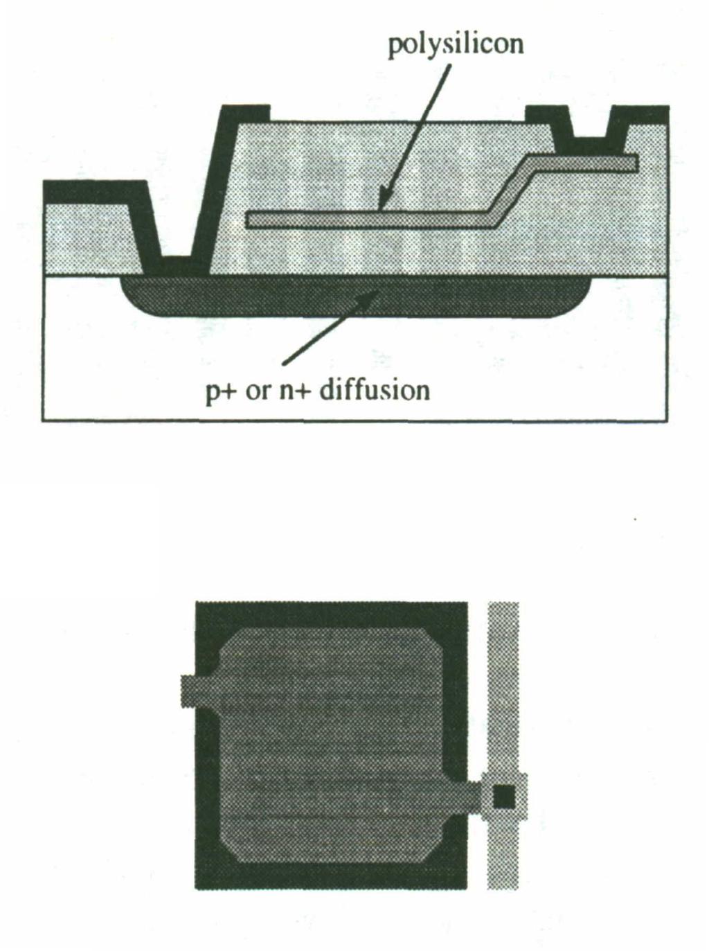
13 Resistor Layout I Resistor types Polysilicon 1 / 2 Diffusion (P + / N + ) Well - used for high value resistors Resistance determine by layer sheet resistance: R=R L/W For linear resistors: Polysilicon is used (other types of resistors are voltage dependent) There is also a problem of maximum signal swing for diffusion & well resistors - require that parasitic p-n junction remains reverse biased For well resistors, substrate diffusions need to be placed in order to achieve insulation between adjacent strips

14 Resistor layouts
15 Resistor Layout II Usually large L-values are required to achieve adequate resistance - use of serpentine structures Main problems: Corners (difficult to estimate actual value - estimated as /2) Undercut causes width reduction - use large width to limit random component undercut variations Undercut is a function of boundary conditions - use dummy strips suitable terminations have to be used (ohmic contacts only ) - depend on resistive layer used resistance variation with position - use common centriod & interdigitized structures temperature effects can be reduced by placing resistors on the same isotherm shielding has to be used in mixed mode ICs

16 Layout of a resistor made by well diffusion

17 Layout of 2 matched interdigitated resistors
18 Matched devices on the same isotherm
19 Capacitor Layout I Layers used for capacitors plates: metal, poly, diffusions Layers used as dielectric silicon oxide or polysilicon oxide Most common linear capacitor (used in SC / SI blocks) Poly1 - Poly2 capacitor Capacitance given by: C = ε 0 ε R A/t (1-10pF typical C) Capacitance value is determined by the smaller plate area For good matching capacitor values should be an integer multiple of some unit capacitor value (usually pf)
20 Polysilicon-diffusion capacitor


21 Layout of two matched capacitors Common Centroid Symmetry

22 Polysilicon-polysilicon capacitor with shielding well
23 Capacitor Layout II Problems associated with integrated capacitors: Undercut effect A* = WL(1-αP/A) i.e actual area affected by Perimeter/Area (P/A) ratio Parasitic capacitance (especially to substrate - can be non-linear) Field fringing effects (often neglected in calculation) In order to achieve good capacitor matching: Use common centroid arrangement Dummy boundary devices Use same P/A ratio in the layout of capacitors whose values are not integer multiples of a unit value Use a protective (shielding) well surrounded by a guard ring (substrate contacts) Use matched metal lines and terminations

24 Layout of a non-integer multiple of a unit capacitor
25 Layout-Oriented Design Determine components to be matched Accuracy should rely on component ratios rather than absolute values Each component should be sized to be an integral number of a unit size Components to be matched should be physically placed near to each other Avoid minimum dimensions on components to be accurately matched Design performance (at least to a first order approximation) should be independent of : temperature V T absolute component values intrinsic transconductance
Fundamentals of ANALOG TO DIGITAL CONVERTERS: Part I.3. Technology
 Fundamentals of ANALOG TO DIGITAL CONVERTERS: Part I.3 Technology January 019 Texas A&M University 1 Spring, 019 Well-Diffusion Resistor Example shows two long resistors for K range Alternatively, serpentine
CMOS Devices. PN junctions and diodes NMOS and PMOS transistors Resistors Capacitors Inductors Bipolar transistors
 CMOS Devices PN junctions and diodes NMOS and PMOS transistors Resistors Capacitors Inductors Bipolar transistors PN Junctions Diffusion causes depletion region D.R. is insulator and establishes barrier
EE382M-14 CMOS Analog Integrated Circuit Design
 EE382M-14 CMOS Analog Integrated Circuit Design Lecture 3, MOS Capacitances, Passive Components, and Layout of Analog Integrated Circuits MOS Capacitances Type of MOS transistor capacitors Depletion capacitance
ECEN 474/704 Lab 2: Layout Design
 ECEN 474/704 Lab 2: Layout esign Objectives Learn Techniques for successful integrated circuit layout design. Introduction In this lab you will learn in detail how to generate a simple transistor layout.
Lecture 210 Physical Aspects of ICs (12/15/01) Page 210-1
 Page 210-1") Lecture 210 Physical Aspects of ICs (12/15/01) Page 210-1 LECTURE 210 PHYSICAL ASPECTS OF ICs (READING: Text-Sec. 2.5, 2.6, 2.8) INTRODUCTION Objective Illustrate the physical aspects of integrated circuits
Lecture 210 Physical Aspects of ICs (12/15/01) Page 210-1 LECTURE 210 PHYSICAL ASPECTS OF ICs (READING: Text-Sec. 2.5, 2.6, 2.8) INTRODUCTION Objective Illustrate the physical aspects of integrated circuits
Lecture 3: CMOS Transistor Theory
 Lecture 3: CMOS Transistor Theory Outline Introduction MOS Capacitor nmos I-V Characteristics pmos I-V Characteristics Gate and Diffusion Capacitance 2 Introduction So far, we have treated transistors
ELEN0037 Microelectronic IC Design. Prof. Dr. Michael Kraft
 ELEN0037 Microelectronic IC Design Prof. Dr. Michael Kraft Lecture 2: Technological Aspects Technology Passive components Active components CMOS Process Basic Layout Scaling CMOS Technology Integrated
Circuits. L5: Fabrication and Layout -2 ( ) B. Mazhari Dept. of EE, IIT Kanpur. B. Mazhari, IITK. G-Number
 B. Mazhari Dept. of EE, IIT Kanpur. B. Mazhari, IITK. G-Number") EE610: CMOS Analog Circuits L5: Fabrication and Layout -2 (12.8.2013) B. Mazhari Dept. of EE, IIT Kanpur 44 Passive Components: Resistor Besides MOS transistors, sometimes one requires to implement passive
EE610: CMOS Analog Circuits L5: Fabrication and Layout -2 (12.8.2013) B. Mazhari Dept. of EE, IIT Kanpur 44 Passive Components: Resistor Besides MOS transistors, sometimes one requires to implement passive
Lecture 11: MOS Transistor
 Lecture 11: MOS Transistor Prof. Niknejad Lecture Outline Review: MOS Capacitors Regions MOS Capacitors (3.8 3.9) CV Curve Threshold Voltage MOS Transistors (4.1 4.3): Overview Cross-section and layout
Lecture 12: MOS Capacitors, transistors. Context
 Lecture 12: MOS Capacitors, transistors Context In the last lecture, we discussed PN diodes, and the depletion layer into semiconductor surfaces. Small signal models In this lecture, we will apply those
MOS Transistor I-V Characteristics and Parasitics
 ECEN454 Digital Integrated Circuit Design MOS Transistor I-V Characteristics and Parasitics ECEN 454 Facts about Transistors So far, we have treated transistors as ideal switches An ON transistor passes
MOSFET: Introduction
 E&CE 437 Integrated VLSI Systems MOS Transistor 1 of 30 MOSFET: Introduction Metal oxide semiconductor field effect transistor (MOSFET) or MOS is widely used for implementing digital designs Its major
an introduction to Semiconductor Devices
 an introduction to Semiconductor Devices Donald A. Neamen Chapter 6 Fundamentals of the Metal-Oxide-Semiconductor Field-Effect Transistor Introduction: Chapter 6 1. MOSFET Structure 2. MOS Capacitor -
EE 434 Lecture 12. Process Flow (wrap up) Device Modeling in Semiconductor Processes
 Device Modeling in Semiconductor Processes") EE 434 Lecture 12 Process Flow (wrap up) Device Modeling in Semiconductor Processes Quiz 6 How have process engineers configured a process to assure that the thickness of the gate oxide for the p-channel
EE 434 Lecture 12 Process Flow (wrap up) Device Modeling in Semiconductor Processes Quiz 6 How have process engineers configured a process to assure that the thickness of the gate oxide for the p-channel
MOS Transistor Theory
 MOS Transistor Theory So far, we have viewed a MOS transistor as an ideal switch (digital operation) Reality: less than ideal EE 261 Krish Chakrabarty 1 Introduction So far, we have treated transistors
2. (2pts) What is the major difference between an epitaxial layer and a polysilicon layer?
 What is the major difference between an epitaxial layer and a polysilicon layer?") EE 330 Exam 1 Spring 2017 Name Instructions: Students may bring 1 page of notes (front and back) to this exam and a calculator but the use of any device that has wireless communication capability is prohibited.
EE 330 Exam 1 Spring 2017 Name Instructions: Students may bring 1 page of notes (front and back) to this exam and a calculator but the use of any device that has wireless communication capability is prohibited.
ESE 570: Digital Integrated Circuits and VLSI Fundamentals
 ESE 570: Digital Integrated Circuits and VLSI Fundamentals Lec 4: January 29, 2019 MOS Transistor Theory, MOS Model Penn ESE 570 Spring 2019 Khanna Lecture Outline! CMOS Process Enhancements! Semiconductor
EE115C Winter 2017 Digital Electronic Circuits. Lecture 3: MOS RC Model, CMOS Manufacturing
 EE115C Winter 2017 Digital Electronic Circuits Lecture 3: MOS RC Model, CMOS Manufacturing Agenda MOS Transistor: RC Model (pp. 104-113) S R on D CMOS Manufacturing Process (pp. 36-46) S S C GS G G C GD
EE 435. Lecture 37. Parasitic Capacitances in MOS Devices. String DAC Parasitic Capacitances
 EE 435 Lecture 37 Parasitic Capacitances in MOS Devices String DAC Parasitic Capacitances Parasitic Capacitors in MOSFET (will initially consider two) Parasitic Capacitors in MOSFET C GCH Parasitic Capacitors
MOS Transistor Properties Review
 MOS Transistor Properties Review 1 VLSI Chip Manufacturing Process Photolithography: transfer of mask patterns to the chip Diffusion or ion implantation: selective doping of Si substrate Oxidation: SiO
ECE 342 Electronic Circuits. Lecture 6 MOS Transistors
 ECE 342 Electronic Circuits Lecture 6 MOS Transistors Jose E. Schutt-Aine Electrical & Computer Engineering University of Illinois jesa@illinois.edu 1 NMOS Transistor Typically L = 0.1 to 3 m, W = 0.2
MOSFET Capacitance Model
 MOSFET Capacitance Model So far we discussed the MOSFET DC models. In real circuit operation, the device operates under time varying terminal voltages and the device operation can be described by: 1 small
University of Pennsylvania Department of Electrical Engineering. ESE 570 Midterm Exam March 14, 2013 FORMULAS AND DATA
 University of Pennsylvania Department of Electrical Engineering ESE 570 Midterm Exam March 4, 03 FORMULAS AND DATA. PHYSICAL CONSTANTS: n i = intrinsic concentration undoped) silicon =.45 x 0 0 cm -3 @
CMOS Cross Section. EECS240 Spring Today s Lecture. Dimensions. CMOS Process. Devices. Lecture 2: CMOS Technology and Passive Devices
 EECS240 Spring 2008 CMOS Cross Section Metal p - substrate p + diffusion Lecture 2: CMOS echnology and Passive Devices Poly n - well n + diffusion Elad Alon Dept. of EECS EECS240 Lecture 2 4 oday s Lecture
CMOS Cross Section. EECS240 Spring Dimensions. Today s Lecture. Why Talk About Passives? EE240 Process
 EECS240 Spring 202 CMOS Cross Section Metal p - substrate p + diffusion Lecture 2: CMOS Technology and Passive Devices Poly n - well n + diffusion Elad Alon Dept. of EECS EECS240 Lecture 2 4 Today s Lecture
Introduction to CMOS VLSI. Chapter 2: CMOS Transistor Theory. Harris, 2004 Updated by Li Chen, Outline
 Introduction to MOS VLSI Design hapter : MOS Transistor Theory copyright@david Harris, 004 Updated by Li hen, 010 Outline Introduction MOS apacitor nmos IV haracteristics pmos IV haracteristics Gate and
SECTION: Circle one: Alam Lundstrom. ECE 305 Exam 5 SOLUTIONS: Spring 2016 April 18, 2016 M. A. Alam and M.S. Lundstrom Purdue University
 NAME: PUID: SECTION: Circle one: Alam Lundstrom ECE 305 Exam 5 SOLUTIONS: April 18, 2016 M A Alam and MS Lundstrom Purdue University This is a closed book exam You may use a calculator and the formula
ESE 570: Digital Integrated Circuits and VLSI Fundamentals
 ESE 570: Digital Integrated Circuits and VLSI Fundamentals Lec 4: January 23, 2018 MOS Transistor Theory, MOS Model Penn ESE 570 Spring 2018 Khanna Lecture Outline! CMOS Process Enhancements! Semiconductor
VLSI Design and Simulation
 VLSI Design and Simulation Performance Characterization Topics Performance Characterization Resistance Estimation Capacitance Estimation Inductance Estimation Performance Characterization Inverter Voltage
Lecture 4: CMOS Transistor Theory
 Introduction to CMOS VLSI Design Lecture 4: CMOS Transistor Theory David Harris, Harvey Mudd College Kartik Mohanram and Steven Levitan University of Pittsburgh Outline q Introduction q MOS Capacitor q
EECS240 Spring Today s Lecture. Lecture 2: CMOS Technology and Passive Devices. Lingkai Kong EECS. EE240 CMOS Technology
 EECS240 Spring 2013 Lecture 2: CMOS Technology and Passive Devices Lingkai Kong EECS Today s Lecture EE240 CMOS Technology Passive devices Motivation Resistors Capacitors (Inductors) Next time: MOS transistor
Class 05: Device Physics II
 Topics: 1. Introduction 2. NFET Model and Cross Section with Parasitics 3. NFET as a Capacitor 4. Capacitance vs. Voltage Curves 5. NFET as a Capacitor - Band Diagrams at V=0 6. NFET as a Capacitor - Accumulation
Lecture 15 OUTLINE. MOSFET structure & operation (qualitative) Review of electrostatics The (N)MOS capacitor
 Review of electrostatics The (N)MOS capacitor") Lecture 15 OUTLINE MOSFET structure & operation (qualitative) Review of electrostatics The (N)MOS capacitor Electrostatics Charge vs. voltage characteristic Reading: Chapter 6.1 6.2.1 EE15 Spring 28 Lecture
Lecture 15 OUTLINE MOSFET structure & operation (qualitative) Review of electrostatics The (N)MOS capacitor Electrostatics Charge vs. voltage characteristic Reading: Chapter 6.1 6.2.1 EE15 Spring 28 Lecture
! CMOS Process Enhancements. ! Semiconductor Physics. " Band gaps. " Field Effects. ! MOS Physics. " Cut-off. " Depletion.
 ESE 570: Digital Integrated Circuits and VLSI Fundamentals Lec 4: January 9, 019 MOS Transistor Theory, MOS Model Lecture Outline CMOS Process Enhancements Semiconductor Physics Band gaps Field Effects
Lecture 040 Integrated Circuit Technology - II (5/11/03) Page ECE Frequency Synthesizers P.E. Allen
 Page ECE Frequency Synthesizers P.E. Allen") Lecture 040 Integrated Circuit Technology - II (5/11/03) Page 040-1 LECTURE 040 INTEGRATED CIRCUIT TECHNOLOGY - II (Reference [7,8]) Objective The objective of this presentation is: 1.) Illustrate and
Lecture 040 Integrated Circuit Technology - II (5/11/03) Page 040-1 LECTURE 040 INTEGRATED CIRCUIT TECHNOLOGY - II (Reference [7,8]) Objective The objective of this presentation is: 1.) Illustrate and
EE105 - Fall 2005 Microelectronic Devices and Circuits
 EE105 - Fall 005 Microelectronic Devices and Circuits ecture 7 MOS Transistor Announcements Homework 3, due today Homework 4 due next week ab this week Reading: Chapter 4 1 ecture Material ast lecture
The Intrinsic Silicon
 The Intrinsic ilicon Thermally generated electrons and holes Carrier concentration p i =n i ni=1.45x10 10 cm-3 @ room temp Generally: n i = 3.1X10 16 T 3/2 e -1.21/2KT cm -3 T= temperature in K o (egrees
EE 434 Lecture 13. Basic Semiconductor Processes Devices in Semiconductor Processes
 EE 434 Lecture 3 Basic Semiconductor Processes Devices in Semiconductor Processes Quiz 9 The top view of a device fabricated in a bulk CMOS process is shown in the figure below a) Identify the device b)
Fundamentals of the Metal Oxide Semiconductor Field-Effect Transistor
 Triode Working FET Fundamentals of the Metal Oxide Semiconductor Field-Effect Transistor The characteristics of energy bands as a function of applied voltage. Surface inversion. The expression for the
Lecture 15 OUTLINE. MOSFET structure & operation (qualitative) Review of electrostatics The (N)MOS capacitor
 Review of electrostatics The (N)MOS capacitor") Lecture 15 OUTLINE MOSFET structure & operation (qualitative) Review of electrostatics The (N)MOS capacitor Electrostatics t ti Charge vs. voltage characteristic Reading: Chapter 6.1 6.2.1 EE105 Fall 2007
Lecture 15 OUTLINE MOSFET structure & operation (qualitative) Review of electrostatics The (N)MOS capacitor Electrostatics t ti Charge vs. voltage characteristic Reading: Chapter 6.1 6.2.1 EE105 Fall 2007
Lecture 5: CMOS Transistor Theory
 Lecture 5: CMOS Transistor Theory Slides courtesy of Deming Chen Slides based on the initial set from David Harris CMOS VLSI Design Outline q q q q q q q Introduction MOS Capacitor nmos I-V Characteristics
Metal-oxide-semiconductor field effect transistors (2 lectures)
") Metal-ide-semiconductor field effect transistors ( lectures) MOS physics (brief in book) Current-voltage characteristics - pinch-off / channel length modulation - weak inversion - velocity saturation -
Metal-ide-semiconductor field effect transistors ( lectures) MOS physics (brief in book) Current-voltage characteristics - pinch-off / channel length modulation - weak inversion - velocity saturation -
CMPEN 411 VLSI Digital Circuits. Lecture 03: MOS Transistor
 CMPEN 411 VLSI Digital Circuits Lecture 03: MOS Transistor Kyusun Choi [Adapted from Rabaey s Digital Integrated Circuits, Second Edition, 2003 J. Rabaey, A. Chandrakasan, B. Nikolic] CMPEN 411 L03 S.1
Fig. 1 CMOS Transistor Circuits (a) Inverter Out = NOT In, (b) NOR-gate C = NOT (A or B)
 Inverter Out = NOT In, (b) NOR-gate C = NOT (A or B)") 1 Introduction to Transistor-Level Logic Circuits 1 By Prawat Nagvajara At the transistor level of logic circuits, transistors operate as switches with the logic variables controlling the open or closed
1 Introduction to Transistor-Level Logic Circuits 1 By Prawat Nagvajara At the transistor level of logic circuits, transistors operate as switches with the logic variables controlling the open or closed
1. The MOS Transistor. Electrical Conduction in Solids
 Electrical Conduction in Solids!The band diagram describes the energy levels for electron in solids.!the lower filled band is named Valence Band.!The upper vacant band is named conduction band.!the distance
MOS Transistors. Prof. Krishna Saraswat. Department of Electrical Engineering Stanford University Stanford, CA
 MOS Transistors Prof. Krishna Saraswat Department of Electrical Engineering S Stanford, CA 94305 saraswat@stanford.edu 1 1930: Patent on the Field-Effect Transistor! Julius Lilienfeld filed a patent describing
Lecture 25. Semiconductor Memories. Issues in Memory
 Lecture 25 Semiconductor Memories Issues in Memory Memory Classification Memory Architectures TheMemoryCore Periphery 1 Semiconductor Memory Classification RWM NVRWM ROM Random Access Non-Random Access
Digital Integrated Circuits A Design Perspective
 Semiconductor Memories Adapted from Chapter 12 of Digital Integrated Circuits A Design Perspective Jan M. Rabaey et al. Copyright 2003 Prentice Hall/Pearson Outline Memory Classification Memory Architectures
EEC 118 Lecture #2: MOSFET Structure and Basic Operation. Rajeevan Amirtharajah University of California, Davis Jeff Parkhurst Intel Corporation
 EEC 118 Lecture #2: MOSFET Structure and Basic Operation Rajeevan Amirtharajah University of California, Davis Jeff Parkhurst Intel Corporation Announcements Lab 1 this week, report due next week Bring
! CMOS Process Enhancements. ! Semiconductor Physics. " Band gaps. " Field Effects. ! MOS Physics. " Cut-off. " Depletion.
 ESE 570: Digital Integrated Circuits and VLSI Fundamentals Lec 4: January 3, 018 MOS Transistor Theory, MOS Model Lecture Outline! CMOS Process Enhancements! Semiconductor Physics " Band gaps " Field Effects!
MOS CAPACITOR AND MOSFET
 EE336 Semiconductor Devices 1 MOS CAPACITOR AND MOSFET Dr. Mohammed M. Farag Ideal MOS Capacitor Semiconductor Devices Physics and Technology Chapter 5 EE336 Semiconductor Devices 2 MOS Capacitor Structure
Lecture 23: Negative Resistance Osc, Differential Osc, and VCOs
 EECS 142 Lecture 23: Negative Resistance Osc, Differential Osc, and VCOs Prof. Ali M. Niknejad University of California, Berkeley Copyright c 2005 by Ali M. Niknejad A. M. Niknejad University of California,
Chapter 2 CMOS Transistor Theory. Jin-Fu Li Department of Electrical Engineering National Central University Jungli, Taiwan
 Chapter 2 CMOS Transistor Theory Jin-Fu Li Department of Electrical Engineering National Central University Jungli, Taiwan Outline Introduction MOS Device Design Equation Pass Transistor Jin-Fu Li, EE,
EE105 - Fall 2006 Microelectronic Devices and Circuits
 EE105 - Fall 2006 Microelectronic Devices and Circuits Prof. Jan M. Rabaey (jan@eecs) Lecture 7: MOS Transistor Some Administrative Issues Lab 2 this week Hw 2 due on We Hw 3 will be posted same day MIDTERM
Lecture 15: MOS Transistor models: Body effects, SPICE models. Context. In the last lecture, we discussed the modes of operation of a MOS FET:
 Lecture 15: MOS Transistor models: Body effects, SPICE models Context In the last lecture, we discussed the modes of operation of a MOS FET: oltage controlled resistor model I- curve (Square-Law Model)
EE 4345 Chapter 6. Derek Johnson Michael Hasni Rex Reeves Michael Custer
 EE 4345 Chapter 6 Derek Johnson Michael Hasni Rex Reeves Michael Custer Coupling AC Signals Constructing timing networks Constructing phase shift networks Feedback loop compensation Semiconductors use:
MOS Transistor Theory
 CHAPTER 3 MOS Transistor Theory Outline 2 1. Introduction 2. Ideal I-V Characteristics 3. Nonideal I-V Effects 4. C-V Characteristics 5. DC Transfer Characteristics 6. Switch-level RC Delay Models MOS
Chapter 4 Field-Effect Transistors
 Chapter 4 Field-Effect Transistors Microelectronic Circuit Design Richard C. Jaeger Travis N. Blalock 5/5/11 Chap 4-1 Chapter Goals Describe operation of MOSFETs. Define FET characteristics in operation
ECE 342 Electronic Circuits. 3. MOS Transistors
 ECE 342 Electronic Circuits 3. MOS Transistors Jose E. Schutt-Aine Electrical & Computer Engineering University of Illinois jschutt@emlab.uiuc.edu 1 NMOS Transistor Typically L = 0.1 to 3 m, W = 0.2 to
VLSI Design The MOS Transistor
 VLSI Design The MOS Transistor Frank Sill Torres Universidade Federal de Minas Gerais (UFMG), Brazil VLSI Design: CMOS Technology 1 Outline Introduction MOS Capacitor nmos I-V Characteristics pmos I-V
ENEE 359a Digital VLSI Design
 SLIDE 1 ENEE 359a Digital VLSI Design & Logical Effort Prof. blj@ece.umd.edu Credit where credit is due: Slides contain original artwork ( Jacob 2004) as well as material taken liberally from Irwin & Vijay
VLSI GATE LEVEL DESIGN UNIT - III P.VIDYA SAGAR ( ASSOCIATE PROFESSOR) Department of Electronics and Communication Engineering, VBIT
 Department of Electronics and Communication Engineering, VBIT") VLSI UNIT - III GATE LEVEL DESIGN P.VIDYA SAGAR ( ASSOCIATE PROFESSOR) contents GATE LEVEL DESIGN : Logic Gates and Other complex gates, Switch logic, Alternate gate circuits, Time Delays, Driving large
VLSI UNIT - III GATE LEVEL DESIGN P.VIDYA SAGAR ( ASSOCIATE PROFESSOR) contents GATE LEVEL DESIGN : Logic Gates and Other complex gates, Switch logic, Alternate gate circuits, Time Delays, Driving large
EE141- Fall 2002 Lecture 27. Memory EE141. Announcements. We finished all the labs No homework this week Projects are due next Tuesday 9am EE141
 - Fall 2002 Lecture 27 Memory Announcements We finished all the labs No homework this week Projects are due next Tuesday 9am 1 Today s Lecture Memory:» SRAM» DRAM» Flash Memory 2 Floating-gate transistor
SEMICONDUCTOR MEMORIES
 SEMICONDUCTOR MEMORIES Semiconductor Memory Classification RWM NVRWM ROM Random Access Non-Random Access EPROM E 2 PROM Mask-Programmed Programmable (PROM) SRAM FIFO FLASH DRAM LIFO Shift Register CAM
Lecture 12 CMOS Delay & Transient Response
 EE 471: Transport Phenomena in Solid State Devices Spring 2018 Lecture 12 CMOS Delay & Transient Response Bryan Ackland Department of Electrical and Computer Engineering Stevens Institute of Technology
MOS Capacitors ECE 2204
 MOS apacitors EE 2204 Some lasses of Field Effect Transistors Metal-Oxide-Semiconductor Field Effect Transistor MOSFET, which will be the type that we will study in this course. Metal-Semiconductor Field
The Physical Structure (NMOS)
") The Physical Structure (NMOS) Al SiO2 Field Oxide Gate oxide S n+ Polysilicon Gate Al SiO2 SiO2 D n+ L channel P Substrate Field Oxide contact Metal (S) n+ (G) L W n+ (D) Poly 1 Transistor Resistance Two
The Physical Structure (NMOS) Al SiO2 Field Oxide Gate oxide S n+ Polysilicon Gate Al SiO2 SiO2 D n+ L channel P Substrate Field Oxide contact Metal (S) n+ (G) L W n+ (D) Poly 1 Transistor Resistance Two
EE141. EE141-Spring 2006 Digital Integrated Circuits. Administrative Stuff. Class Material. Flash Memory. Read-Only Memory Cells MOS OR ROM
 EE141-pring 2006 igital Integrated Circuits Lecture 29 Flash memory Administrative tuff reat job on projects and posters! Homework #10 due today Lab reports due this week Friday lab in 353 Final exam May
Digital Integrated Circuits A Design Perspective. Semiconductor. Memories. Memories
 Digital Integrated Circuits A Design Perspective Semiconductor Chapter Overview Memory Classification Memory Architectures The Memory Core Periphery Reliability Case Studies Semiconductor Memory Classification
VLSI VLSI CIRCUIT DESIGN PROCESSES P.VIDYA SAGAR ( ASSOCIATE PROFESSOR) Department of Electronics and Communication Engineering, VBIT
 Department of Electronics and Communication Engineering, VBIT") VLSI VLSI CIRCUIT DESIGN PROCESSES P.VIDYA SAGAR ( ASSOCIATE PROFESSOR) SYLLABUS UNIT II VLSI CIRCUIT DESIGN PROCESSES: VLSI Design Flow, MOS Layers, Stick Diagrams, Design Rules and Layout, 2 m CMOS Design
VLSI VLSI CIRCUIT DESIGN PROCESSES P.VIDYA SAGAR ( ASSOCIATE PROFESSOR) SYLLABUS UNIT II VLSI CIRCUIT DESIGN PROCESSES: VLSI Design Flow, MOS Layers, Stick Diagrams, Design Rules and Layout, 2 m CMOS Design
Operation and Modeling of. The MOS Transistor. Second Edition. Yannis Tsividis Columbia University. New York Oxford OXFORD UNIVERSITY PRESS
 Operation and Modeling of The MOS Transistor Second Edition Yannis Tsividis Columbia University New York Oxford OXFORD UNIVERSITY PRESS CONTENTS Chapter 1 l.l 1.2 1.3 1.4 1.5 1.6 1.7 Chapter 2 2.1 2.2
6.012 Electronic Devices and Circuits Spring 2005
 6.012 Electronic Devices and Circuits Spring 2005 May 16, 2005 Final Exam (200 points) -OPEN BOOK- Problem NAME RECITATION TIME 1 2 3 4 5 Total General guidelines (please read carefully before starting):
EE105 Fall 2014 Microelectronic Devices and Circuits. NMOS Transistor Capacitances: Saturation Region
 EE105 Fall 014 Microelectronic Devices and Circuits Prof. Ming C. Wu wu@eecs.berkeley.edu 511 Sutardja Dai Hall (SDH) 1 NMOS Transistor Capacitances: Saturation Region Drain no longer connected to channel
Semiconductor memories
 Semiconductor memories Semiconductor Memories Data in Write Memory cell Read Data out Some design issues : How many cells? Function? Power consuption? Access type? How fast are read/write operations? Semiconductor
ECEN474: (Analog) VLSI Circuit Design Fall 2010
 VLSI Circuit Design Fall 2010") ECEN474: (Analog) VLSI Circuit Design Fall 2010 Lecture 6: Layout Techniques Sam Palermo Analog & Mixed-Signal Center Texas A&M University Announcements Lab 2 next week Has a prelab Upgrading Cadence version
ECEN474: (Analog) VLSI Circuit Design Fall 2010 Lecture 6: Layout Techniques Sam Palermo Analog & Mixed-Signal Center Texas A&M University Announcements Lab 2 next week Has a prelab Upgrading Cadence version
! MOS Capacitances. " Extrinsic. " Intrinsic. ! Lumped Capacitance Model. ! First Order Capacitor Summary. ! Capacitance Implications
 ESE 570: Digital Integrated Circuits and VLSI Fundamentals Lec 7: February, 07 MOS SPICE Models, MOS Parasitic Details Lecture Outline! MOS Capacitances " Extrinsic " Intrinsic! Lumped Capacitance Model!
Topics to be Covered. capacitance inductance transmission lines
 Topics to be Covered Circuit Elements Switching Characteristics Power Dissipation Conductor Sizes Charge Sharing Design Margins Yield resistance capacitance inductance transmission lines Resistance of
Charge Storage in the MOS Structure. The Inverted MOS Capacitor (V GB > V Tn )
") The Inverted MO Capacitor (V > V Tn ) We consider the surface potential as Þxed (ÒpinnedÓ) at φ s,max = - φ p φ(x).5 V. V V ox Charge torage in the MO tructure Three regions of operation: Accumulation:
The Inverted MO Capacitor (V > V Tn ) We consider the surface potential as Þxed (ÒpinnedÓ) at φ s,max = - φ p φ(x).5 V. V V ox Charge torage in the MO tructure Three regions of operation: Accumulation:
Integrated Circuits & Systems
 Federal University of Santa Catarina Center for Technology Computer Science & Electronics Engineering Integrated Circuits & Systems INE 5442 Lecture 10 MOSFET part 1 guntzel@inf.ufsc.br ual-well Trench-Isolated
ECEN474: (Analog) VLSI Circuit Design Fall 2012
 VLSI Circuit Design Fall 2012") ECEN474: (Analog) VLSI Circuit Design Fall 2012 Lecture 5: Layout Techniques Sam Palermo Analog & Mixed-Signal Center Texas A&M University Announcements HW1 due today at 5PM For grad students, confirm
ECEN474: (Analog) VLSI Circuit Design Fall 2012 Lecture 5: Layout Techniques Sam Palermo Analog & Mixed-Signal Center Texas A&M University Announcements HW1 due today at 5PM For grad students, confirm
ELEC 3908, Physical Electronics, Lecture 26. MOSFET Small Signal Modelling
 ELEC 3908, Physical Electronics, Lecture 26 MOSFET Small Signal Modelling Lecture Outline MOSFET small signal behavior will be considered in the same way as for the diode and BJT Capacitances will be considered
Capacitors Diodes Transistors. PC200 Lectures. Terry Sturtevant. Wilfrid Laurier University. June 4, 2009
 Wilfrid Laurier University June 4, 2009 Capacitor an electronic device which consists of two conductive plates separated by an insulator Capacitor an electronic device which consists of two conductive
Low Power VLSI Circuits and Systems Prof. Ajit Pal Department of Computer Science and Engineering Indian Institute of Technology, Kharagpur
 Low Power VLSI Circuits and Systems Prof. Ajit Pal Department of Computer Science and Engineering Indian Institute of Technology, Kharagpur Lecture No. # 08 MOS Inverters - III Hello, and welcome to today
LECTURE 3 MOSFETS II. MOS SCALING What is Scaling?
 LECTURE 3 MOSFETS II Lecture 3 Goals* * Understand constant field and constant voltage scaling and their effects. Understand small geometry effects for MOS transistors and their implications modeling and
nmos IC Design Report Module: EEE 112
 nmos IC Design Report Author: 1302509 Zhao Ruimin Module: EEE 112 Lecturer: Date: Dr.Zhao Ce Zhou June/5/2015 Abstract This lab intended to train the experimental skills of the layout designing of the
Semiconductor Memories
 Semiconductor References: Adapted from: Digital Integrated Circuits: A Design Perspective, J. Rabaey UCB Principles of CMOS VLSI Design: A Systems Perspective, 2nd Ed., N. H. E. Weste and K. Eshraghian
ECE 497 JS Lecture - 12 Device Technologies
 ECE 497 JS Lecture - 12 Device Technologies Spring 2004 Jose E. Schutt-Aine Electrical & Computer Engineering University of Illinois jose@emlab.uiuc.edu 1 NMOS Transistor 2 ρ Source channel charge density
Course Administration. CPE/EE 427, CPE 527 VLSI Design I L04: MOS Transistors. Review: CMOS Process at a Glance
 Course Administration CPE/EE 7, CPE 7 VLI esign I L: MO Transistors epartment of Electrical and Computer Engineering University of Alabama in Huntsville Aleksandar Milenkovic ( www.ece.uah.edu/~milenka
Lecture 0: Introduction
 Lecture 0: Introduction Introduction q Integrated circuits: many transistors on one chip q Very Large Scale Integration (VLSI): bucketloads! q Complementary Metal Oxide Semiconductor Fast, cheap, low power
Semiconductor Physics fall 2012 problems
 Semiconductor Physics fall 2012 problems 1. An n-type sample of silicon has a uniform density N D = 10 16 atoms cm -3 of arsenic, and a p-type silicon sample has N A = 10 15 atoms cm -3 of boron. For each
ECEN474/704: (Analog) VLSI Circuit Design Fall 2016
 VLSI Circuit Design Fall 2016") ECEN474/704: (Analog) VLSI Circuit Design Fall 016 Lecture 5: Layout Techniques Sam Palermo Analog & Mixed-Signal Center Texas A&M University Announcements Exam1 is on 9/9 It will be in WEB 36C :0-3:45PM
ECEN474/704: (Analog) VLSI Circuit Design Fall 016 Lecture 5: Layout Techniques Sam Palermo Analog & Mixed-Signal Center Texas A&M University Announcements Exam1 is on 9/9 It will be in WEB 36C :0-3:45PM
ECE-305: Fall 2017 MOS Capacitors and Transistors
 ECE-305: Fall 2017 MOS Capacitors and Transistors Pierret, Semiconductor Device Fundamentals (SDF) Chapters 15+16 (pp. 525-530, 563-599) Professor Peter Bermel Electrical and Computer Engineering Purdue
AE74 VLSI DESIGN JUN 2015
 Q.2 a. Write down the different levels of integration of IC industry. (4) b. With neat sketch explain briefly PMOS & NMOS enhancement mode transistor. N-MOS enhancement mode transistor:- This transistor
Electronics Fets and Mosfets Prof D C Dube Department of Physics Indian Institute of Technology, Delhi
 Electronics Fets and Mosfets Prof D C Dube Department of Physics Indian Institute of Technology, Delhi Module No. #05 Lecture No. #02 FETS and MOSFETS (contd.) In the previous lecture, we studied the working
Lecture 020 Review of CMOS Technology (09/01/03) Page 020-1
 Page 020-1") Lecture 020 Review of CMOS Technology (09/01/03) Page 020-1 LECTURE 020 REVIEW OF CMOS TECHNOLOGY INTRODUCTION Objective Provide sufficient background to understand the limits and capabilities of CMOS
Lecture 020 Review of CMOS Technology (09/01/03) Page 020-1 LECTURE 020 REVIEW OF CMOS TECHNOLOGY INTRODUCTION Objective Provide sufficient background to understand the limits and capabilities of CMOS
The Devices: MOS Transistors
 The Devices: MOS Transistors References: Semiconductor Device Fundamentals, R. F. Pierret, Addison-Wesley Digital Integrated Circuits: A Design Perspective, J. Rabaey et.al. Prentice Hall NMOS Transistor
MOS Transistor Theory MOSFET Symbols Current Characteristics of MOSFET. MOS Symbols and Characteristics. nmos Enhancement Transistor
 MOS Transistor Theory MOSFET Symbols Current Characteristics of MOSFET Calculation of t and Important 2 nd Order Effects SmallSignal Signal MOSFET Model Summary Material from: CMOS LSI Design By Weste
The Inverter. Digital Integrated Circuits A Design Perspective. Jan M. Rabaey Anantha Chandrakasan Borivoje Nikolic
 Digital Integrated Circuits A Design Perspective Jan M. Rabaey Anantha Chandrakasan Borivoje Nikolic The Inverter Revised from Digital Integrated Circuits, Jan M. Rabaey el, 2003 Propagation Delay CMOS
Scaling Issues in Planar FET: Dual Gate FET and FinFETs
 Scaling Issues in Planar FET: Dual Gate FET and FinFETs Lecture 12 Dr. Amr Bayoumi Fall 2014 Advanced Devices (EC760) Arab Academy for Science and Technology - Cairo 1 Outline Scaling Issues for Planar
VLSI Design I; A. Milenkovic 1
 Review: implified CMO Inverter Process CPE/EE 7, CPE 7 VLI esign I L: MO Transistor cut line epartment of Electrical and Computer Engineering University of Alabama in Huntsville Aleksandar Milenkovic (