Sadayuki Yoshitomi. Semiconductor Company 2007/01/25
|
|
|
- Lauren McBride
- 5 years ago
- Views:
Transcription

1 Sadayuki Yoshitomi. Semiconductor Company Copyright 2006, Toshiba Corporation. ASP-DAC 2007
 on silicon. 2. Utilize very-accurate compact model. Looking at the EKV3.0 MOSFET Model. Accuracy of conductance.")
2 . Make the best of Electro-Magnetic (EM) simulation. Is EM simulator applicable for silicon technology? EM simulator enables accurate modeling of passive devices (Inductor and MIM capacitor ) on silicon. 2. Utilize very-accurate compact model. Looking at the EKV3.0 MOSFET Model. Accuracy of conductance. NS effects. 3. Use the Co-simulation Technique for final evaluation. Case:CMOS Amplifier Case2:CMOS VCO Case3:BiCMOS LNA 2
 3")
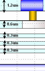
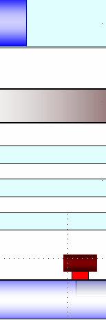
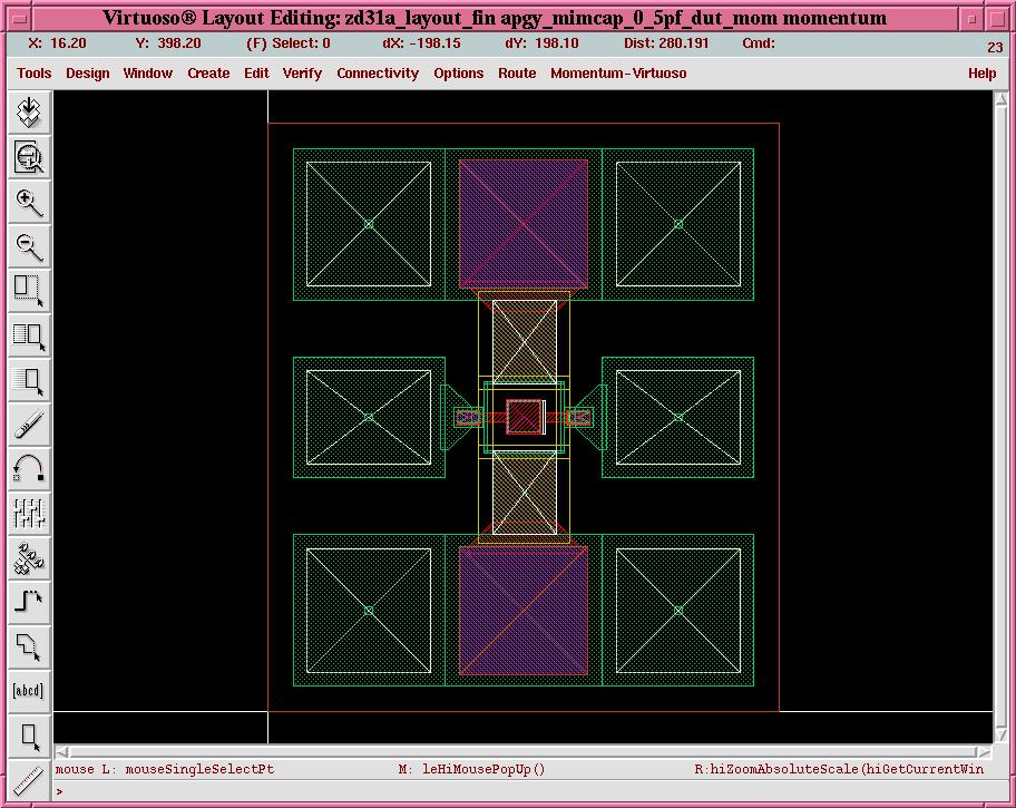
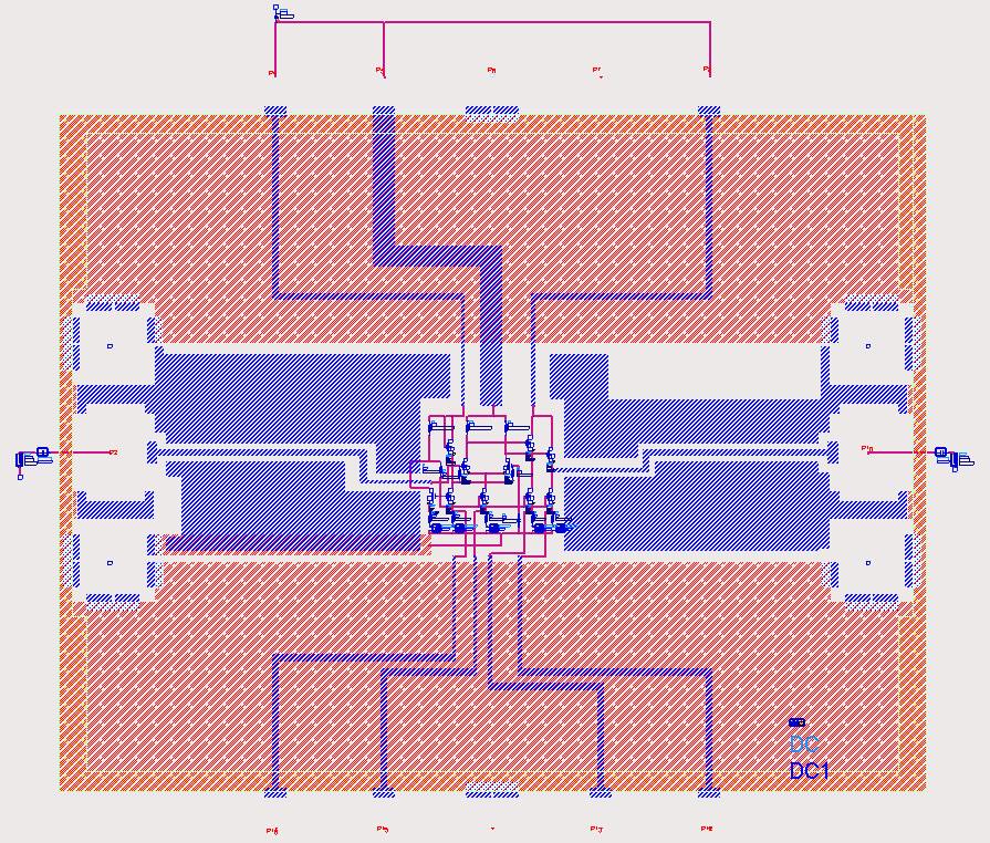
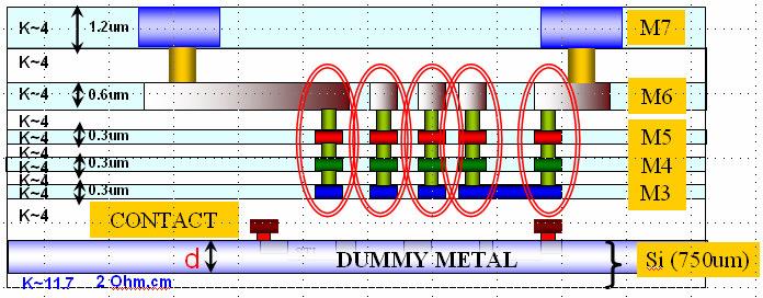
3 A A K~.7.2um 0.6um 0.3um 0.3um 0.3um CONTACT 2 Ohm.cm d STI DUMMY METAL M7 M6 M5 M4 M3 Si (750um) 3

4 Open-PAD 0.~0.0GHz 4

5 Z SUB Z jωc ox = jωc SUB + R SUB 5
6 !"#$ Low Frequency C ox - imagz [ ] R [ ] SUB realz SUB 6
7 !#"#$ High Frequency C SUB = ω R SUB R SUB real ( ) Z SUB 7
8 %&()*+, Insert the metal layer (thickness d ) that covers silicon substrate. This metal layer has the same conductivity as the silicon substrate. Total thickness of silicon substrate should keep the original value. w.o DUMMY Metal Measurement w.o DUMMY Metal Measurement D=50um D=60um D=70um D=80um D=90um D=50um D=60um D=70um D=80um D=90um 8
9 -. &/0 ## $%& #()$*&!" #!" +$%& %$)& 9


10 -.2um M7 0.6um 0.3um 0.3um 0.3um!"#$ % CONTACT STI DUMMY METAL,#!"-,.#!"- /$ 2 M6 M5 M4 M3 & & 0
11 3. Simulator Setup Agilent s RFDE Momentum (2005A or later) 50MHz-26.5GHz (max) RF Mode Mesh Frequency 26.5GHz 20 Cells/Wavelength 3D=ON, Thickconductor=ON, EDGE Mesh=Off Dedicated setup for DUMMY Layers 3D=OFF Thickconductor=OFF EDGE Mesh=ON
12 20um %& S-Parameters & -factor 66um!! #! 2
13 4./ ()0$(ω.()0$ +.(ω / ()$,-.((,-$,-,- ()$(*(ω(+./ (,-$(ω 3
14 -&- Ls (50MHz) Rs (50MHz) Cox(54MHz) Rsub(9.8GHz) Momentum.06 nh.23 Ohm ff 36.9 Ohm Measurement.07 nh.26 Ohm ff 28.3 Ohm 4

15 #%&5 &!! + 5
16 % 6 & 6
 on silicon. 2. Utilize very-accurate compact model. Looking at the EKV3.0 MOSFET Model. Accuracy of conductance.")
17 . Make the best of Electro-Magnetic (EM) simulation. Is EM simulator applicable for silicon technology? EM simulator enables accurate modeling of passive devices (Inductor and MIM capacitor ) on silicon. 2. Utilize very-accurate compact model. Looking at the EKV3.0 MOSFET Model. Accuracy of conductance. NS effects. 3. Use the Co-simulation Technique for final evaluation. Case:CMOS Amplifier Case2:CMOS VCO Case3:BiCMOS LNA 7
18 - -& W.Grabinski MOS-AK, IWCM2007 No. of Model Parameters earlyekv BSIM4v4 BSIM3v3 MMv2 BSIM3v2 HiSIM.2.0 BSIM2 HSP28 BSIM3v3 BSIM BSIM3v2 BSIM4 BSIM2 PCIM HSP28 SP BSIM3v MM9 LEVEL2 BSIM EKV3 EKV2.6 LEVEL3 EKV LEVEL Including L,W,P scaling Without scaling Years Number of DC model parameters vs. the year of the introduction of the model Most recent versions of the EKV, HiSIM, MMand SP models are included Significant growth of the parameter number that includes geometry (W/L) scaling 8
19 *&73&- W.Grabinski MOS-AK, IWCM2007 No. of Model Parameters earlyekv BSIM4v4 BSIM3v3 MMv2 BSIM3v2 HiSIM.2.0 BSIM2 HSP28 BSIM3v3 BSIM BSIM3v2 BSIM4 BSIM2 PCIM HSP28 SP BSIM3v MM9 LEVEL2 BSIM EKV3 EKV2.6 LEVEL3 EKV LEVEL Including L,W,P scaling Without scaling Years Independent mosfet model development based on the roots of the semiconductor physics and the design driven EKV modeling methodology EKV3 preserves coherent charge-based framework for static/dynamic modeling 9
20 &738!"#$ A.Bazigos, EKV3.0 model code & parameter extraction, EKV user meeting/workshop, Nov4-5,
21 &738!#"#$ A.Bazigos, EKV3.0 model code & parameter extraction, EKV user meeting/workshop, Nov4-5,
22 -738&!"$ Started from classic current transport equation I D = µ W I dψ dx s + U T d I dx Description of Ψs by using linearized I dψs = dx n C ox d dx i 2 ID formula with linearized I I D = µ W n i C ox d dx I + U T di dx 3 22
23 23 L x I D x I s = = 0-738&!#"$ -738&!#"$ 4 Inversion charge densities at source and drain Integration of (3) 5 R F id T ox id is T ox is I T I ox i D I I U C n U C n L W d U d C n L W I id is id is + + = + = µ µ 6 7 ( ) ( ) ( ) + µ = D is T ox D is R F U C n L W I 2 2 Diffusion Drift
24 2 * g ch = di dv ch = q i = 4 + i 2 = i G i G i = 4 + i + 2 0nm, 40nm, 0.6um CMOS Technologies included. 24
25 29 & Creating the segmentation of long-channel MOSFETs. General concepts can be found Take finite time for charge to travel throughout the channel. Distribution effect Memory effect 25
26 738&:;4 NMOS CGB BackGate PMOS CGB BackGate 26
27 ;-<: 3>#$%& ()*)+#,(+-)!"##$%& ()*)+#,(+-) /( /( *// // (/ (/ (/ (/ (/ 0(/ 0(/ S 0(/ 0(/ (/ (/ /( /( 0/( 0/(!.!. /( /( /( /( /( 0/( 0/( /( /( 0/( 0/(!"##$%+& ()*)+#,(+-) (/ /( /( /( Lg=2.0um Lg=0.um (6,(7*//8 (6,(7//8 49(5 (6,(7*//8 (6,(7//8 49(5!"##$%& ()*)+#,(+-)* ( 0( 0 0( 0( 0 9: 9; 9< 9( 9 0 9: 9; 2!. 9< 4%5 9( 9!. 4%5!"##$%+& ()*)+#,(+-)*3 ( db(s2) 738 & 3> #$%& ()*)+#,(+-)*3 2 *// // (/ 0(/ (/ (/ 0(/ S /( 0/(!. /( /( 0/( /( 0/( (6,(7*//8 (6,(7//8 49(5 ; - = db(s2) ( 2 9: 9; 9< 9( 9!. 4%5 Vg = 0.4 Volts, Vds=0.2,0.3,0.5,0.8,. and.4volts. 27
28 : 0 Capacitances CGB 0 Rg EKV3.0 Scaling Ratio [A.U] CFGD,CFGS CJDB,CJDS Scaling Ratio [A.U] Measured Lg [um] Lg [um] 0 00 RSUB,RSUB4 0 RSUB2,RSUB3 Scaling Ratio [A.U] 0 Measured EKV3.0 Scaling Ratio [A.U] Measured EKV Lg [um] 0 0. Lg [um] 0 28
29 . Make the best of Electro-Magnetic (EM) simulation. Is EM simulator applicable for silicon technology? EM simulator enables accurate modeling of passive devices (Inductor and MIM capacitor ) on silicon. 2. Utilize very-accurate compact model. Looking at the EKV3.0 MOSFET Model. Accuracy of conductance. NS effects. 3. Use the Co-simulation Technique for final evaluation. Case:CMOS Amplifier Case2:CMOS VCO Case3:BiCMOS LNA 29

30 = - 2 /!! $ 30
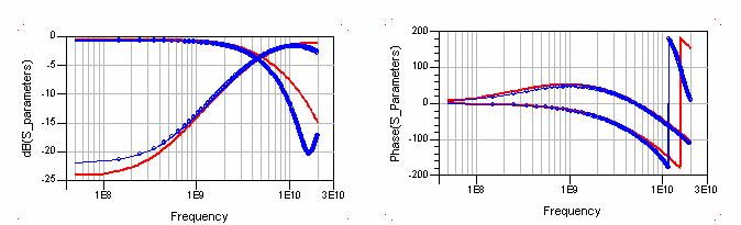
31 Reasonable match has been observed. Further need to improve S2 accuracy!

32 CMOS Power VCO #=#>? 3 5 %29:

33 ; - Transistors -EKV model- 33
34 :!*27+$ Initial simulation with Lumped L model!! Oscillation frequency differs by 0.35 GHz EM-Cosim helps predict circuit behavior with an ultimate accuracy 34


35 = ;+2!6>?$ :; -< &%- <.A 35

36 ; - B-& 36
37 3. &,! 0! +-%23 -+-%23 3 C: 37
38 Simulation Technique for RF-CMOS circuit design. Next generation of Compact Model Provides better accurate conductance and high-frequency behavior. Make the best of Electromagnetic Tools Doing more practice helps to overcome inaccuracy. Worth trying DUMMY METAL. If successful in PAD, successful in EM-Cosim, too.!+;< ; = 38
EKV MOS Transistor Modelling & RF Application
 HP-RF MOS Modelling Workshop, Munich, February 15-16, 1999 EKV MOS Transistor Modelling & RF Application Matthias Bucher, Wladek Grabinski Electronics Laboratory (LEG) Swiss Federal Institute of Technology,
Analysis of Transconductances in Deep Submicron CMOS with EKV 3.0
 MOS Models & Parameter Extraction Workgroup Arbeitskreis MOS Modelle & Parameterextraktion XFAB, Erfurt, Germany, October 2, 2002 Analysis of Transconductances in Deep Submicron CMOS with EKV 3.0 Matthias
Investigation of the Thermal Noise of MOS Transistors under Analog and RF Operating Conditions
 Investigation of the Thermal Noise of MOS Transistors under Analog and RF Operating Conditions Ralf Brederlow 1, Georg Wenig 2, and Roland Thewes 1 1 Infineon Technologies, Corporate Research, 2 Technical
Microelectronics Part 1: Main CMOS circuits design rules
 GBM8320 Dispositifs Médicaux telligents Microelectronics Part 1: Main CMOS circuits design rules Mohamad Sawan et al. Laboratoire de neurotechnologies Polystim! http://www.cours.polymtl.ca/gbm8320/! med-amine.miled@polymtl.ca!
6.012 Electronic Devices and Circuits Spring 2005
 6.012 Electronic Devices and Circuits Spring 2005 May 16, 2005 Final Exam (200 points) -OPEN BOOK- Problem NAME RECITATION TIME 1 2 3 4 5 Total General guidelines (please read carefully before starting):
Advanced Compact Models for MOSFETs
 Advanced Compact Models for MOSFETs Christian Enz, Carlos Galup-Montoro, Gennady Gildenblat, Chenming Hu, Ronald van Langevelde, Mitiko Miura-Mattausch, Rafael Rios, Chih-Tang (Tom) Sah Josef Watts (editor)
Lecture 3: CMOS Transistor Theory
 Lecture 3: CMOS Transistor Theory Outline Introduction MOS Capacitor nmos I-V Characteristics pmos I-V Characteristics Gate and Diffusion Capacitance 2 Introduction So far, we have treated transistors
SECTION: Circle one: Alam Lundstrom. ECE 305 Exam 5 SOLUTIONS: Spring 2016 April 18, 2016 M. A. Alam and M.S. Lundstrom Purdue University
 NAME: PUID: SECTION: Circle one: Alam Lundstrom ECE 305 Exam 5 SOLUTIONS: April 18, 2016 M A Alam and MS Lundstrom Purdue University This is a closed book exam You may use a calculator and the formula
Device Models (PN Diode, MOSFET )
") Device Models (PN Diode, MOSFET ) Instructor: Steven P. Levitan steve@ece.pitt.edu TA: Gayatri Mehta, José Martínez Book: Digital Integrated Circuits: A Design Perspective; Jan Rabaey Lab Notes: Handed
Device Models (PN Diode, MOSFET ) Instructor: Steven P. Levitan steve@ece.pitt.edu TA: Gayatri Mehta, José Martínez Book: Digital Integrated Circuits: A Design Perspective; Jan Rabaey Lab Notes: Handed
Lecture 23: Negative Resistance Osc, Differential Osc, and VCOs
 EECS 142 Lecture 23: Negative Resistance Osc, Differential Osc, and VCOs Prof. Ali M. Niknejad University of California, Berkeley Copyright c 2005 by Ali M. Niknejad A. M. Niknejad University of California,
Lecture 15: MOS Transistor models: Body effects, SPICE models. Context. In the last lecture, we discussed the modes of operation of a MOS FET:
 Lecture 15: MOS Transistor models: Body effects, SPICE models Context In the last lecture, we discussed the modes of operation of a MOS FET: oltage controlled resistor model I- curve (Square-Law Model)
The PSP compact MOSFET model An update
 The PSP compact MOSFET model An update Gert-Jan Smit, Andries Scholten, D.B.M. Klaassen NXP Semiconductors Ronald van Langevelde Philips Research Europe Gennady Gildenblat, Weimin Wu, Xin Li, Amit Jha,
Fundamentals of the Metal Oxide Semiconductor Field-Effect Transistor
 Triode Working FET Fundamentals of the Metal Oxide Semiconductor Field-Effect Transistor The characteristics of energy bands as a function of applied voltage. Surface inversion. The expression for the
EE 330 Lecture 17. MOSFET Modeling CMOS Process Flow
 EE 330 Lecture 17 MOSFET Modeling CMOS Process Flow Review from Last Lecture Limitations of Existing Models V DD V OUT V OUT V DD?? V IN V OUT V IN V IN V DD Switch-Level Models V DD Simple square-law
ECE 546 Lecture 11 MOS Amplifiers
 ECE 546 Lecture MOS Amplifiers Spring 208 Jose E. Schutt-Aine Electrical & Computer Engineering University of Illinois jesa@illinois.edu ECE 546 Jose Schutt Aine Amplifiers Definitions Used to increase
Characterization and modeling of RF-MOSFETs in the millimeter-wave frequency domain. Sadayuki Yoshitomi, Fumie Fujii
 MOS-AK //03 Characterization and modeling of RF-MOSFETs in the millimeter-wave frequency domain Sadayuki Yoshitomi, Fumie Fujii Semiconductor & Storage Products Company Toshiba Corporation Copyright 03,
Lecture 4: CMOS Transistor Theory
 Introduction to CMOS VLSI Design Lecture 4: CMOS Transistor Theory David Harris, Harvey Mudd College Kartik Mohanram and Steven Levitan University of Pittsburgh Outline q Introduction q MOS Capacitor q
Lecture 040 Integrated Circuit Technology - II (5/11/03) Page ECE Frequency Synthesizers P.E. Allen
 Page ECE Frequency Synthesizers P.E. Allen") Lecture 040 Integrated Circuit Technology - II (5/11/03) Page 040-1 LECTURE 040 INTEGRATED CIRCUIT TECHNOLOGY - II (Reference [7,8]) Objective The objective of this presentation is: 1.) Illustrate and
Lecture 040 Integrated Circuit Technology - II (5/11/03) Page 040-1 LECTURE 040 INTEGRATED CIRCUIT TECHNOLOGY - II (Reference [7,8]) Objective The objective of this presentation is: 1.) Illustrate and
The Devices. Digital Integrated Circuits A Design Perspective. Jan M. Rabaey Anantha Chandrakasan Borivoje Nikolic. July 30, 2002
 Digital Integrated Circuits A Design Perspective Jan M. Rabaey Anantha Chandrakasan Borivoje Nikolic The Devices July 30, 2002 Goal of this chapter Present intuitive understanding of device operation Introduction
Device Models (PN Diode, MOSFET )
") Device Models (PN Diode, MOSFET ) Instructor: Steven P. Levitan steve@ece.pitt.edu TA: Gayatri Mehta, José Martínez Book: Digital Integrated Circuits: A Design Perspective; Jan Rabaey Lab Notes: Handed
Device Models (PN Diode, MOSFET ) Instructor: Steven P. Levitan steve@ece.pitt.edu TA: Gayatri Mehta, José Martínez Book: Digital Integrated Circuits: A Design Perspective; Jan Rabaey Lab Notes: Handed
CMOS Devices. PN junctions and diodes NMOS and PMOS transistors Resistors Capacitors Inductors Bipolar transistors
 CMOS Devices PN junctions and diodes NMOS and PMOS transistors Resistors Capacitors Inductors Bipolar transistors PN Junctions Diffusion causes depletion region D.R. is insulator and establishes barrier
Integrated Circuits & Systems
 Federal University of Santa Catarina Center for Technology Computer Science & Electronics Engineering Integrated Circuits & Systems INE 5442 Lecture 10 MOSFET part 1 guntzel@inf.ufsc.br ual-well Trench-Isolated
EECS240 Spring Today s Lecture. Lecture 2: CMOS Technology and Passive Devices. Lingkai Kong EECS. EE240 CMOS Technology
 EECS240 Spring 2013 Lecture 2: CMOS Technology and Passive Devices Lingkai Kong EECS Today s Lecture EE240 CMOS Technology Passive devices Motivation Resistors Capacitors (Inductors) Next time: MOS transistor
EE 330 Lecture 16. MOS Device Modeling p-channel n-channel comparisons Model consistency and relationships CMOS Process Flow
 EE 330 Lecture 16 MOS Device Modeling p-channel n-channel comparisons Model consistency and relationships CMOS Process Flow Review from Last Time Operation Regions by Applications Id I D 300 250 200 150
MOSFET: Introduction
 E&CE 437 Integrated VLSI Systems MOS Transistor 1 of 30 MOSFET: Introduction Metal oxide semiconductor field effect transistor (MOSFET) or MOS is widely used for implementing digital designs Its major
6.776 High Speed Communication Circuits Lecture 10 Noise Modeling in Amplifiers
 6.776 High Speed Communication Circuits Lecture 10 Noise Modeling in Amplifiers Michael Perrott Massachusetts Institute of Technology March 8, 2005 Copyright 2005 by Michael H. Perrott Notation for Mean,
ECE 342 Electronic Circuits. Lecture 6 MOS Transistors
 ECE 342 Electronic Circuits Lecture 6 MOS Transistors Jose E. Schutt-Aine Electrical & Computer Engineering University of Illinois jesa@illinois.edu 1 NMOS Transistor Typically L = 0.1 to 3 m, W = 0.2
1. (50 points, BJT curves & equivalent) For the 2N3904 =(npn) and the 2N3906 =(pnp)
 For the 2N3904 =(npn) and the 2N3906 =(pnp)") HW 3 1. (50 points, BJT curves & equivalent) For the 2N3904 =(npn) and the 2N3906 =(pnp) a) Obtain in Spice the transistor curves given on the course web page except do in separate plots, one for the npn
HW 3 1. (50 points, BJT curves & equivalent) For the 2N3904 =(npn) and the 2N3906 =(pnp) a) Obtain in Spice the transistor curves given on the course web page except do in separate plots, one for the npn
ESE570 Spring University of Pennsylvania Department of Electrical and System Engineering Digital Integrated Cicruits AND VLSI Fundamentals
 University of Pennsylvania Department of Electrical and System Engineering Digital Integrated Cicruits AND VLSI Fundamentals ESE570, Spring 2018 Final Monday, Apr 0 5 Problems with point weightings shown.
MOS Transistors. Prof. Krishna Saraswat. Department of Electrical Engineering Stanford University Stanford, CA
 MOS Transistors Prof. Krishna Saraswat Department of Electrical Engineering S Stanford, CA 94305 saraswat@stanford.edu 1 1930: Patent on the Field-Effect Transistor! Julius Lilienfeld filed a patent describing
EE 330 Lecture 16. Devices in Semiconductor Processes. MOS Transistors
 EE 330 Lecture 16 Devices in Semiconductor Processes MOS Transistors Review from Last Time Model Summary I D I V DS V S I B V BS = 0 0 VS VT W VDS ID = μcox VS VT VDS VS V VDS VS VT L T < W μc ( V V )
Analytical Optimization of High Performance and High Quality Factor MEMS Spiral Inductor
 Progress In Electromagnetics Research M, Vol. 34, 171 179, 2014 Analytical Optimization of High Performance and High Quality Factor MEMS Spiral Inductor Parsa Pirouznia * and Bahram Azizollah Ganji Abstract
EKV Modelling of MOS Varactors and LC Tank Oscillator Design
 EKV Modelling of MOS Varactors and LC Tank Oscillator Design Wolfgang Mathis TET Leibniz Universität Hannover Jan-K. Bremer NXP Hamburg MOS-AK Workshop 01 6. 7. April 01, Dresden Content: Motivation: VCO
Self-heat Modeling of Multi-finger n-mosfets for RF-CMOS Applications
 Self-heat Modeling of Multi-finger n-mosfets for RF-CMOS Applications Hitoshi Aoki and Haruo Kobayashi Faculty of Science and Technology, Gunma University (RMO2D-3) Outline Research Background Purposes
ECE 342 Electronic Circuits. 3. MOS Transistors
 ECE 342 Electronic Circuits 3. MOS Transistors Jose E. Schutt-Aine Electrical & Computer Engineering University of Illinois jschutt@emlab.uiuc.edu 1 NMOS Transistor Typically L = 0.1 to 3 m, W = 0.2 to
EE 330 Lecture 18. Small-signal Model (very preliminary) Bulk CMOS Process Flow
 Bulk CMOS Process Flow") EE 330 Lecture 18 Small-signal Model (very preliminary) Bulk CMOS Process Flow Review from Last Lecture How many models of the MOSFET do we have? Switch-level model (2) Square-law model Square-law model
EE 330 Lecture 18 Small-signal Model (very preliminary) Bulk CMOS Process Flow Review from Last Lecture How many models of the MOSFET do we have? Switch-level model (2) Square-law model Square-law model
Lecture 210 Physical Aspects of ICs (12/15/01) Page 210-1
 Page 210-1") Lecture 210 Physical Aspects of ICs (12/15/01) Page 210-1 LECTURE 210 PHYSICAL ASPECTS OF ICs (READING: Text-Sec. 2.5, 2.6, 2.8) INTRODUCTION Objective Illustrate the physical aspects of integrated circuits
Lecture 210 Physical Aspects of ICs (12/15/01) Page 210-1 LECTURE 210 PHYSICAL ASPECTS OF ICs (READING: Text-Sec. 2.5, 2.6, 2.8) INTRODUCTION Objective Illustrate the physical aspects of integrated circuits
Digital Integrated Circuits A Design Perspective. Jan M. Rabaey Anantha Chandrakasan Borivoje Nikolic. The Devices. July 30, Devices.
 Digital Integrated Circuits A Design Perspective Jan M. Rabaey Anantha Chandrakasan Borivoje Nikolic The July 30, 2002 1 Goal of this chapter Present intuitive understanding of device operation Introduction
University of Pennsylvania Department of Electrical Engineering. ESE 570 Midterm Exam March 14, 2013 FORMULAS AND DATA
 University of Pennsylvania Department of Electrical Engineering ESE 570 Midterm Exam March 4, 03 FORMULAS AND DATA. PHYSICAL CONSTANTS: n i = intrinsic concentration undoped) silicon =.45 x 0 0 cm -3 @
MOSFET Capacitance Model
 MOSFET Capacitance Model So far we discussed the MOSFET DC models. In real circuit operation, the device operates under time varying terminal voltages and the device operation can be described by: 1 small
Fig. 1 CMOS Transistor Circuits (a) Inverter Out = NOT In, (b) NOR-gate C = NOT (A or B)
 Inverter Out = NOT In, (b) NOR-gate C = NOT (A or B)") 1 Introduction to Transistor-Level Logic Circuits 1 By Prawat Nagvajara At the transistor level of logic circuits, transistors operate as switches with the logic variables controlling the open or closed
1 Introduction to Transistor-Level Logic Circuits 1 By Prawat Nagvajara At the transistor level of logic circuits, transistors operate as switches with the logic variables controlling the open or closed
Lecture 12: MOSFET Devices
 Lecture 12: MOSFET Devices Gu-Yeon Wei Division of Engineering and Applied Sciences Harvard University guyeon@eecs.harvard.edu Wei 1 Overview Reading S&S: Chapter 5.1~5.4 Supplemental Reading Background
Lecture 12: MOS Capacitors, transistors. Context
 Lecture 12: MOS Capacitors, transistors Context In the last lecture, we discussed PN diodes, and the depletion layer into semiconductor surfaces. Small signal models In this lecture, we will apply those
MOS Transistor Theory
 CHAPTER 3 MOS Transistor Theory Outline 2 1. Introduction 2. Ideal I-V Characteristics 3. Nonideal I-V Effects 4. C-V Characteristics 5. DC Transfer Characteristics 6. Switch-level RC Delay Models MOS
Compact Modeling of Ultra Deep Submicron CMOS Devices
 Compact Modeling of Ultra Deep Submicron CMOS Devices Wladyslaw Grabinski*, Matthias Bucher, Jean-Michel Sallese, François Krummenacher Swiss Federal Institute of Technology (EPFL), Electronics Laboratory,
MOS Transistor Properties Review
 MOS Transistor Properties Review 1 VLSI Chip Manufacturing Process Photolithography: transfer of mask patterns to the chip Diffusion or ion implantation: selective doping of Si substrate Oxidation: SiO
The Devices: MOS Transistors
 The Devices: MOS Transistors References: Semiconductor Device Fundamentals, R. F. Pierret, Addison-Wesley Digital Integrated Circuits: A Design Perspective, J. Rabaey et.al. Prentice Hall NMOS Transistor
Topics to be Covered. capacitance inductance transmission lines
 Topics to be Covered Circuit Elements Switching Characteristics Power Dissipation Conductor Sizes Charge Sharing Design Margins Yield resistance capacitance inductance transmission lines Resistance of
Practice 3: Semiconductors
 Practice 3: Semiconductors Digital Electronic Circuits Semester A 2012 VLSI Fabrication Process VLSI Very Large Scale Integration The ability to fabricate many devices on a single substrate within a given
3. Basic building blocks. Analog Design for CMOS VLSI Systems Franco Maloberti
 Inverter with active load It is the simplest gain stage. The dc gain is given by the slope of the transfer characteristics. Small signal analysis C = C gs + C gs,ov C 2 = C gd + C gd,ov + C 3 = C db +
ECE 497 JS Lecture - 12 Device Technologies
 ECE 497 JS Lecture - 12 Device Technologies Spring 2004 Jose E. Schutt-Aine Electrical & Computer Engineering University of Illinois jose@emlab.uiuc.edu 1 NMOS Transistor 2 ρ Source channel charge density
MOSFET Model with Simple Extraction Procedures, Suitable for Sensitive Analog Simulations
 ROMANIAN JOURNAL OF INFORMATION SCIENCE AND TECHNOLOGY Volume 10, Number 2, 2007, 189 197 MOSFET Model with Simple Extraction Procedures, Suitable for Sensitive Analog Simulations S. EFTIMIE 1, ALEX. RUSU
Workshop WMB. Noise Modeling
 Workshop WMB Noise Modeling Manfred Berroth, Markus Grözing, Stefan Heck, Alexander Bräckle University of Stuttgart, Germany WMB (IMS) Parameter Extraction Strategies For Compact Transistor Models IMS
ECE-343 Test 2: Mar 21, :00-8:00, Closed Book. Name : SOLUTION
 ECE-343 Test 2: Mar 21, 2012 6:00-8:00, Closed Book Name : SOLUTION 1. (25 pts) (a) Draw a circuit diagram for a differential amplifier designed under the following constraints: Use only BJTs. (You may
Operation and Modeling of. The MOS Transistor. Second Edition. Yannis Tsividis Columbia University. New York Oxford OXFORD UNIVERSITY PRESS
 Operation and Modeling of The MOS Transistor Second Edition Yannis Tsividis Columbia University New York Oxford OXFORD UNIVERSITY PRESS CONTENTS Chapter 1 l.l 1.2 1.3 1.4 1.5 1.6 1.7 Chapter 2 2.1 2.2
RFIC2017 MO2B-2. A Simplified CMOS FET Model using Surface Potential Equations For Inter-modulation Simulations of Passive-Mixer-Like Circuits
 A Simplified CMOS FET Model using Surface Potential Equations For Inter-modulation Simulations of Passive-Mixer-Like Circuits M. Baraani Dastjerdi and H. Krishnaswamy CoSMIC Lab, Columbia University, New
Section 12: Intro to Devices
 Section 12: Intro to Devices Extensive reading materials on reserve, including Robert F. Pierret, Semiconductor Device Fundamentals EE143 Ali Javey Bond Model of Electrons and Holes Si Si Si Si Si Si Si
EE 330. Lecture 35. Parasitic Capacitances in MOS Devices
 EE 330 Lecture 35 Parasitic Capacitances in MOS Devices Exam 2 Wed Oct 24 Exam 3 Friday Nov 16 Review from Last Lecture Cascode Configuration Discuss V CC gm1 gm1 I B VCC V OUT g02 g01 A - β β VXX Q 2
Lecture 11: MOS Transistor
 Lecture 11: MOS Transistor Prof. Niknejad Lecture Outline Review: MOS Capacitors Regions MOS Capacitors (3.8 3.9) CV Curve Threshold Voltage MOS Transistors (4.1 4.3): Overview Cross-section and layout
ELEN0037 Microelectronic IC Design. Prof. Dr. Michael Kraft
 ELEN0037 Microelectronic IC Design Prof. Dr. Michael Kraft Lecture 2: Technological Aspects Technology Passive components Active components CMOS Process Basic Layout Scaling CMOS Technology Integrated
Part 4: Heterojunctions - MOS Devices. MOSFET Current Voltage Characteristics
 MOS Device Uses: Part 4: Heterojunctions - MOS Devices MOSCAP capacitor: storing charge, charge-coupled device (CCD), etc. MOSFET transistor: switch, current amplifier, dynamic random access memory (DRAM-volatile),
EE 330 Lecture 16. MOSFET Modeling CMOS Process Flow
 EE 330 Lecture 16 MOSFET Modeling CMOS Process Flow Model Extensions 300 Id 250 200 150 100 50 300 0 0 1 2 3 4 5 Vds Existing Model 250 200 Id 150 100 50 Slope is not 0 0 0 1 2 3 4 Actual Device Vds Model
A Multi-Gate CMOS Compact Model BSIMMG
 A Multi-Gate CMOS Compact Model BSIMMG Darsen Lu, Sriramkumar Venugopalan, Tanvir Morshed, Yogesh Singh Chauhan, Chung-Hsun Lin, Mohan Dunga, Ali Niknejad and Chenming Hu University of California, Berkeley
Today s lecture. EE141- Spring 2003 Lecture 4. Design Rules CMOS Inverter MOS Transistor Model
 - Spring 003 Lecture 4 Design Rules CMOS Inverter MOS Transistor Model Today s lecture Design Rules The CMOS inverter at a glance An MOS transistor model for manual analysis Important! Labs start next
Accurate Modeling of Spiral Inductors on Silicon From Within Cadence Virtuoso using Planar EM Simulation. Agilent EEsof RFIC Seminar Spring 2004
 Accurate Modeling of Spiral Inductors on Silicon From Within Cadence Virtuoso using Planar EM Simulation Agilent EEsof RFIC Seminar Spring Overview Spiral Inductor Models Availability & Limitations Momentum
ESE 570: Digital Integrated Circuits and VLSI Fundamentals
 ESE 570: Digital Integrated Circuits and VLSI Fundamentals Lec 4: January 23, 2018 MOS Transistor Theory, MOS Model Penn ESE 570 Spring 2018 Khanna Lecture Outline! CMOS Process Enhancements! Semiconductor
Studio 3 Review MOSFET as current source Small V DS : Resistor (value controlled by V GS ) Large V DS : Current source (value controlled by V GS )
 Large V DS : Current source (value controlled by V GS )") Studio 3 Review MOSFET as current source Small V DS : Resistor (value controlled by V GS ) Large V DS : Current source (value controlled by V GS ) 1 Simulation Review: Circuit Fixed V GS, Sweep V DS I
Studio 3 Review MOSFET as current source Small V DS : Resistor (value controlled by V GS ) Large V DS : Current source (value controlled by V GS ) 1 Simulation Review: Circuit Fixed V GS, Sweep V DS I
Introduction. HFSS 3D EM Analysis S-parameter. Q3D R/L/C/G Extraction Model. magnitude [db] Frequency [GHz] S11 S21 -30
![Introduction. HFSS 3D EM Analysis S-parameter. Q3D R/L/C/G Extraction Model. magnitude [db] Frequency [GHz] S11 S21 -30](/thumbs/81/83311716.jpg "Introduction. HFSS 3D EM Analysis S-parameter. Q3D R/L/C/G Extraction Model. magnitude [db] Frequency [GHz] S11 S21 -30") ANSOFT Q3D TRANING Introduction HFSS 3D EM Analysis S-parameter Q3D R/L/C/G Extraction Model 0-5 -10 magnitude [db] -15-20 -25-30 S11 S21-35 0 1 2 3 4 5 6 7 8 9 10 Frequency [GHz] Quasi-static or full-wave
ANSOFT Q3D TRANING Introduction HFSS 3D EM Analysis S-parameter Q3D R/L/C/G Extraction Model 0-5 -10 magnitude [db] -15-20 -25-30 S11 S21-35 0 1 2 3 4 5 6 7 8 9 10 Frequency [GHz] Quasi-static or full-wave
ECE-305: Fall 2017 MOS Capacitors and Transistors
 ECE-305: Fall 2017 MOS Capacitors and Transistors Pierret, Semiconductor Device Fundamentals (SDF) Chapters 15+16 (pp. 525-530, 563-599) Professor Peter Bermel Electrical and Computer Engineering Purdue
Introduction and Background
 Analog CMOS Integrated Circuit Design Introduction and Background Dr. Jawdat Abu-Taha Department of Electrical and Computer Engineering Islamic University of Gaza jtaha@iugaza.edu.ps 1 Marking Assignments
EE5311- Digital IC Design
 EE5311- Digital IC Design Module 1 - The Transistor Janakiraman V Assistant Professor Department of Electrical Engineering Indian Institute of Technology Madras Chennai October 28, 2017 Janakiraman, IITM
EEC 118 Lecture #2: MOSFET Structure and Basic Operation. Rajeevan Amirtharajah University of California, Davis Jeff Parkhurst Intel Corporation
 EEC 118 Lecture #2: MOSFET Structure and Basic Operation Rajeevan Amirtharajah University of California, Davis Jeff Parkhurst Intel Corporation Announcements Lab 1 this week, report due next week Bring
Field effect = Induction of an electronic charge due to an electric field Example: Planar capacitor
 JFETs AND MESFETs Introduction Field effect = Induction of an electronic charge due to an electric field Example: Planar capacitor Why would an FET made of a planar capacitor with two metal plates, as
EE 240B Spring Advanced Analog Integrated Circuits Lecture 2: MOS Transistor Models. Elad Alon Dept. of EECS
 EE 240B Spring 2018 Advanced Analog Integrated Circuits Lecture 2: MOS Transistor Models Elad Alon Dept. of EECS Square Law Model? Assumptions made to come up with this model: Charge density determined
Lecture 23 - Frequency Resp onse of Amplifiers (I) Common-Source Amplifier. May 6, 2003
 Common-Source Amplifier. May 6, 2003") 6.0 Microelectronic Devices and Circuits Spring 003 Lecture 3 Lecture 3 Frequency Resp onse of Amplifiers (I) CommonSource Amplifier May 6, 003 Contents:. Intro duction. Intrinsic frequency resp onse of
6.0 Microelectronic Devices and Circuits Spring 003 Lecture 3 Lecture 3 Frequency Resp onse of Amplifiers (I) CommonSource Amplifier May 6, 003 Contents:. Intro duction. Intrinsic frequency resp onse of
Lecture 10 MOSFET (III) MOSFET Equivalent Circuit Models
 MOSFET Equivalent Circuit Models") Lecture 10 MOSFET (III) MOSFET Equivalent Circuit Models Outline Lowfrequency smallsignal equivalent circuit model Highfrequency smallsignal equivalent circuit model Reading Assignment: Howe and Sodini;
Lecture 10 MOSFET (III) MOSFET Equivalent Circuit Models Outline Lowfrequency smallsignal equivalent circuit model Highfrequency smallsignal equivalent circuit model Reading Assignment: Howe and Sodini;
Lecture 11: MOSFET Modeling
 Digital Integrated Circuits (83-313) Lecture 11: MOSFET ing Semester B, 2016-17 Lecturer: Dr. Adam Teman TAs: Itamar Levi, Robert Giterman 18 June 2017 Disclaimer: This course was prepared, in its entirety,
Lecture 23 Frequency Response of Amplifiers (I) Common Source Amplifier. December 1, 2005
 Common Source Amplifier. December 1, 2005") 6.02 Microelectronic Devices and Circuits Fall 2005 Lecture 23 Lecture 23 Frequency Response of Amplifiers (I) Common Source Amplifier December, 2005 Contents:. Introduction 2. Intrinsic frequency response
6.02 Microelectronic Devices and Circuits Fall 2005 Lecture 23 Lecture 23 Frequency Response of Amplifiers (I) Common Source Amplifier December, 2005 Contents:. Introduction 2. Intrinsic frequency response
CMOS Digital Integrated Circuits Lec 13 Semiconductor Memories
 Lec 13 Semiconductor Memories 1 Semiconductor Memory Types Semiconductor Memories Read/Write (R/W) Memory or Random Access Memory (RAM) Read-Only Memory (ROM) Dynamic RAM (DRAM) Static RAM (SRAM) 1. Mask
Homework Assignment #5 EE 477 Spring 2017 Professor Parker
 Homework Assignment #5 EE 477 Spring 2017 Professor Parker Question 1: (15%) Compute the worst-case rising and falling RC time constants at point B of the circuit below using the Elmore delay method. Assume
ESE 570: Digital Integrated Circuits and VLSI Fundamentals
 ESE 570: Digital Integrated Circuits and VLSI Fundamentals Lec 5: January 25, 2018 MOS Operating Regions, pt. 1 Lecture Outline! 3 Regions of operation for MOSFET " Subthreshold " Linear " Saturation!
A Novel Tunable Dual-Band Bandstop Filter (DBBSF) Using BST Capacitors and Tuning Diode
 Using BST Capacitors and Tuning Diode") Progress In Electromagnetics Research C, Vol. 67, 59 69, 2016 A Novel Tunable Dual-Band Bandstop Filter (DBBSF) Using BST Capacitors and Tuning Diode Hassan Aldeeb and Thottam S. Kalkur * Abstract A novel
Progress In Electromagnetics Research C, Vol. 67, 59 69, 2016 A Novel Tunable Dual-Band Bandstop Filter (DBBSF) Using BST Capacitors and Tuning Diode Hassan Aldeeb and Thottam S. Kalkur * Abstract A novel
Low Noise Amplifiers. Prepared by: Heng Zhang. ECEN 665 (ESS) : RF Communication Circuits and Systems
 : RF Communication Circuits and Systems") ECEN 665 (ESS) : RF Communication Circuits and Systems Low Noise Amplifiers Prepared by: Heng Zhang Part of the material here provided is based on Dr. Chunyu Xin s and Dr. Xiaohua Fan s dissertation 1
ECEN 665 (ESS) : RF Communication Circuits and Systems Low Noise Amplifiers Prepared by: Heng Zhang Part of the material here provided is based on Dr. Chunyu Xin s and Dr. Xiaohua Fan s dissertation 1
Circuits. L5: Fabrication and Layout -2 ( ) B. Mazhari Dept. of EE, IIT Kanpur. B. Mazhari, IITK. G-Number
 B. Mazhari Dept. of EE, IIT Kanpur. B. Mazhari, IITK. G-Number") EE610: CMOS Analog Circuits L5: Fabrication and Layout -2 (12.8.2013) B. Mazhari Dept. of EE, IIT Kanpur 44 Passive Components: Resistor Besides MOS transistors, sometimes one requires to implement passive
EE610: CMOS Analog Circuits L5: Fabrication and Layout -2 (12.8.2013) B. Mazhari Dept. of EE, IIT Kanpur 44 Passive Components: Resistor Besides MOS transistors, sometimes one requires to implement passive
Analysis and Design of Analog Integrated Circuits Lecture 14. Noise Spectral Analysis for Circuit Elements
 Analysis and Design of Analog Integrated Circuits Lecture 14 Noise Spectral Analysis for Circuit Elements Michael H. Perrott March 18, 01 Copyright 01 by Michael H. Perrott All rights reserved. Recall
6.012 Electronic Devices and Circuits
 Page 1 of 10 YOUR NAME Department of Electrical Engineering and Computer Science Massachusetts Institute of Technology 6.012 Electronic Devices and Circuits Exam No. 2 Thursday, November 5, 2009 7:30 to
EKV based L-DMOS Model update including internal temperatures
 ROBUSPIC (IST-507653) Deliverable D1.2 EKV based L-DMOS Model update including internal temperatures Yogesh Singh Chauhan, Costin Anghel, Francois Krummenacher, Adrian Ionescu and Michel Declercq Ecole
EECS 105: FALL 06 FINAL
 University of California College of Engineering Department of Electrical Engineering and Computer Sciences Jan M. Rabaey TuTh 2-3:30 Wednesday December 13, 12:30-3:30pm EECS 105: FALL 06 FINAL NAME Last
EECS130 Integrated Circuit Devices
 EECS130 Integrated Circuit Devices Professor Ali Javey 10/30/2007 MOSFETs Lecture 4 Reading: Chapter 17, 19 Announcements The next HW set is due on Thursday. Midterm 2 is next week!!!! Threshold and Subthreshold
MOS Transistor I-V Characteristics and Parasitics
 ECEN454 Digital Integrated Circuit Design MOS Transistor I-V Characteristics and Parasitics ECEN 454 Facts about Transistors So far, we have treated transistors as ideal switches An ON transistor passes
Lecture 10 MOSFET (III) MOSFET Equivalent Circuit Models
 MOSFET Equivalent Circuit Models") Lecture 1 MOSFET (III) MOSFET Equivalent Circuit Models Outline Lowfrequency smallsignal equivalent circuit model Highfrequency smallsignal equivalent circuit model Reading Assignment: Howe and Sodini;
Lecture 1 MOSFET (III) MOSFET Equivalent Circuit Models Outline Lowfrequency smallsignal equivalent circuit model Highfrequency smallsignal equivalent circuit model Reading Assignment: Howe and Sodini;
Choice of V t and Gate Doping Type
 Choice of V t and Gate Doping Type To make circuit design easier, it is routine to set V t at a small positive value, e.g., 0.4 V, so that, at V g = 0, the transistor does not have an inversion layer and
CHAPTER 3: TRANSISTOR MOSFET DR. PHAM NGUYEN THANH LOAN. Hà Nội, 9/24/2012
 1 CHAPTER 3: TRANSISTOR MOSFET DR. PHAM NGUYEN THANH LOAN Hà Nội, 9/24/2012 Chapter 3: MOSFET 2 Introduction Classifications JFET D-FET (Depletion MOS) MOSFET (Enhancement E-FET) DC biasing Small signal
3D Stacked Buck Converter with SrTiO 3 (STO) Capacitors on Silicon Interposer
 Capacitors on Silicon Interposer") 3D Stacked Buck Converter with SrTiO 3 (STO) Capacitors on Silicon Interposer Makoto Takamiya 1, Koichi Ishida 1, Koichi Takemura 2,3, and Takayasu Sakurai 1 1 University of Tokyo, Japan 2 NEC Corporation,
3D Stacked Buck Converter with SrTiO 3 (STO) Capacitors on Silicon Interposer Makoto Takamiya 1, Koichi Ishida 1, Koichi Takemura 2,3, and Takayasu Sakurai 1 1 University of Tokyo, Japan 2 NEC Corporation,
MIXDES 2001 Zakopane, POLAND June 2001
 8 th International Conference ADVANCEMENTS IN DC AND RF MOSFET MODELING WITH THE EPFL-EKV CHARGE BASED MODEL,;(' '(6,* J.-M. SALLESE *, W. GRABINSKI **, A.S. PORRET *, M. BUCHER +, C. LALLEMENT ++, F.
Lecture 04 Review of MOSFET
 ECE 541/ME 541 Microelectronic Fabrication Techniques Lecture 04 Review of MOSFET Zheng Yang (ERF 3017, email: yangzhen@uic.edu) What is a Transistor? A Switch! An MOS Transistor V GS V T V GS S Ron D
TOSHIBA Field Effect Transistor Silicon N Channel MOS Type SSM3K17FU
 SSMK7FU TOSHIBA Field Effect Transistor Silicon N Channel MOS Type SSMK7FU High Speed Switching Applications Analog Switch Applications Unit: mm Suitable for high-density mounting due to compact package
EE382M-14 CMOS Analog Integrated Circuit Design
 EE382M-14 CMOS Analog Integrated Circuit Design Lecture 3, MOS Capacitances, Passive Components, and Layout of Analog Integrated Circuits MOS Capacitances Type of MOS transistor capacitors Depletion capacitance
Accurate Estimating Simultaneous Switching Noises by Using Application Specific Device Modeling
 Accurate Estimating Simultaneous Switching Noises by Using Application Specific Device Modeling Li Ding and Pinaki Mazumder Department of Electrical Engineering and Computer Science The University of Michigan,
VLSI GATE LEVEL DESIGN UNIT - III P.VIDYA SAGAR ( ASSOCIATE PROFESSOR) Department of Electronics and Communication Engineering, VBIT
 Department of Electronics and Communication Engineering, VBIT") VLSI UNIT - III GATE LEVEL DESIGN P.VIDYA SAGAR ( ASSOCIATE PROFESSOR) contents GATE LEVEL DESIGN : Logic Gates and Other complex gates, Switch logic, Alternate gate circuits, Time Delays, Driving large
VLSI UNIT - III GATE LEVEL DESIGN P.VIDYA SAGAR ( ASSOCIATE PROFESSOR) contents GATE LEVEL DESIGN : Logic Gates and Other complex gates, Switch logic, Alternate gate circuits, Time Delays, Driving large