EE 330 Lecture 18. Small-signal Model (very preliminary) Bulk CMOS Process Flow
|
|
|
- Elijah Stanley
- 5 years ago
- Views:
Transcription
1 EE 330 Lecture 18 Small-signal Model (very preliminary) Bulk CMOS Process Flow
2 Review from Last Lecture How many models of the MOSFET do we have? Switch-level model (2) Square-law model Square-law model (with λ and bulk additions) α-law model (with λ and bulk additions) BSIM model BSIM model (with binning extensions) BSIM model (with binning extensions and process corners)
3 Review from Last Lecture The Modeling Challenge I D Actual Modeled with one model V GS3 (and W/L variations or Process Variations) Local Agreement with Any Model V GS2 (and W/L variations or Process Variations) V GS1 (and W/L variations or Process Variations) V DS (and W/L variations or Process Variations) I G I D V DS I = f V,V D 1 GS DS I = f V,V G 2 GS DS I = f V,V B 3 GS DS V GS I B V BS = 0 Difficult to obtain analytical functions that accurately fit actual devices over bias, size, and process variations
4 Review from Last Lecture Model Status Simple dc Model Square-Law Model Small Signal Better Analytical dc Model Sophisticated Model for Computer Simulations BSIM Model Square-Law Model (with extensions for λ,γ effects) Short-Channel α-law Model Frequency Dependent Small Signal Simpler dc Model Switch-Level Models Ideal switches R SW and C GS

5 Review from Last Lecture D n-channel. p-channel modeling D S S G G G G S D S D D D G B G B S S G I G V GS I D D I B B V BS V DS V GS G I G S B I B V BS V DS S I D D I D V GS4 V GS3 Models essentially the same with different signs and model parameters 1 V GS V GS V DS VDS VGS4 VGS3 VGS2 V GS1> 0 0 VGS VTn W V L 2 W 2 μ C V V V V V V V 2L I =I =0 DS I μ C V V V V V V V V D n OX GS Tn DS GS Tn DS GS Tn G B n OX GS Tn GS Tn DS GS Tn 0 V V GS Tp W V L 2 W 2L I =I =0 DS I -μ C V V V V V V V V D p OX GS Tp DS GS Tp DS GS Tp G B 2 -μ C p OX VGS VTp VGS VTp VDS VGS VTp
6 Review from Last Lecture Model Relationships G D R SWn C GSn V GS Determine R SW and C GS in the switch-level model for an n-channel MOSFET from square-law model in the 0.5u ON CMOS process if L=1u, W=1u (Assume μc OX =100μAV -2, C OX =2.5fFu -2,V T0 =1V, V DD =3.5V, V SS =0) S 0 V V GS T W V L 2 W 2L DS I μc V V V V V V V V D OX GS T DS GS T DS GS T 2 μc V V V V V V V OX GS T GS T DS GS T when SW is on, operation is deep triode
7 Review from Last Lecture Model Relationships G D R SWn C GSn V GS Determine R SW and C GS for an n-channel MOSFET from square-law model in the 0.5u ON CMOS process if L=1u, W=1u (Assume μc OX =100μAV -2, C OX =2.5fFu -2,V T0 =1V, V DD =3.5V, V SS =0) When on operating in deep triode W V W L 2 L DS I μc V V V μc V V V D OX GS T DS OX GS T DS V 1 1 DS R = 4K SQ I W 1 D V GS =VDD μc V V ( E 4) OX GS T L V GS =3.5V 1 S C GS = C OX WL = (2.5fFµ -2 )(1µ 2 ) = 2.5fF
8 Review from Last Lecture Model Relationships G D C GSp R SWp V GS Determine R SW and C GS for an p-channel MOSFET from square-law model in the 0.5u ON CMOS process if L=1u, W=1u ( C OX =2.5fFu -2,V T0 =1V, V DD =3.5V, V SS =0) Observe µ n \ µ p 3 S 0 V V GS T W V L 2 W 2L DS -I μc V V V V V V V V D OX GS T DS GS T DS GS T 2 μc V V V V V V V OX GS T GS T DS GS T When SW is on, operation is deep triode
9 Review from Last Lecture Model Relationships D G R SWp C GSp V GS Determine R SW and C GS for an p-channel MOSFET from square-law model in the 0.5u ON CMOS process if L=1u, W=1u Observe µ n \ µ p 3 ( C OX =2.5fFu -2,V T0 =1V, V DD =3.5V, V SS =0) W V W L 2 L DS -I μ C V V V μ C V V V D p OX GS T DS p OX GS T DS -V 1 1 DS R = 12K SQ -I W 1 1 D V GS =VDD μ C V V ( 4) p OX GS T L E V GS =3.5V 3 1 C GS = C OX WL = (2.5fFµ -2 )(1µ 2 ) = 2.5fF Observe the resistance of the p-channel device is approximately 3 times larger than that of the n-channel device for same bias and dimensions! S
10 Modeling of the MOSFET Goal: Obtain a mathematical relationship between the port variables of a device. I f V,V,V I I D G B 1 f f 2 3 GS DS BS VGS,V DS,VBS V GS,V DS,VBS Drain V DS I D I B Gate Bulk I D Simple dc Model V GS V BS Small Signal Better Analytical dc Model Sophisticated Model for Computer Simulations Frequency Dependent Small Signal Simpler dc Model
11 Small-Signal Model Goal with small signal model is to predict performance of circuit or device in the vicinity of an operating point Operating point is often termed Q-point
12 Small-Signal Model y Y Q Q-point X Q x Analytical expressions for small signal model will be developed later
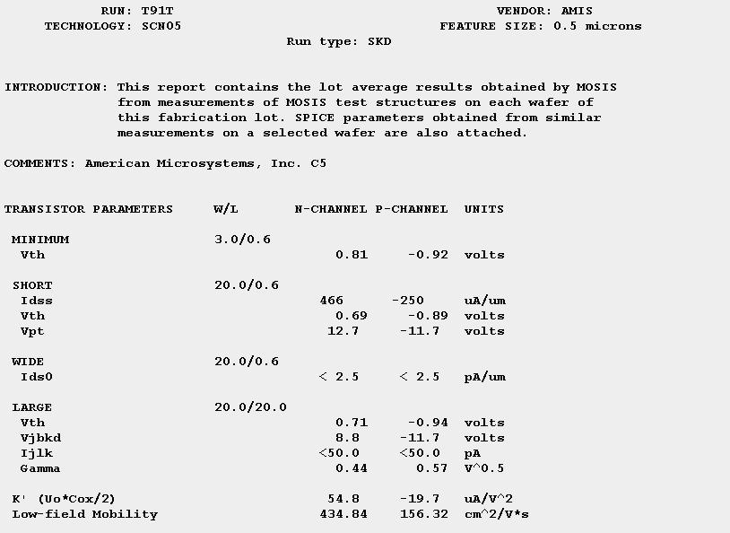
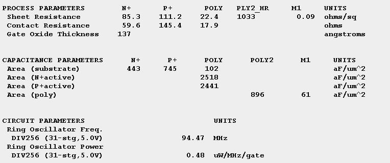
13 Technology Files Design Rules Process Flow (Fabrication Technology) Model Parameters
14 n-well n-well n- p-
15
16
17 Bulk CMOS Process Description n-well process Single Metal Only Depicted Double Poly This type of process dominates what is used for high-volume lowcost processing of integrated circuits today Many process variants and specialized processes are used for lowervolume or niche applications Emphasis in this course will be on the electronics associated with the design of integrated electronic circuits in processes targeting highvolume low-cost products where competition based upon price differentiation may be acute Basic electronics concepts, however, are applicable for lower-volume or niche applicaitons
18 Components Shown n-channel MOSFET p-channel MOSFET Poly Resistor Doubly Poly Capacitor
19 C D A A B B C D
20 Consider Basic Components Only Well Contacts and Guard Rings Will be Discussed Later
21 A A B B
22 A A B B
23 Metal details hidden to reduce clutter A A D G S B D B S B n-channel MOSFET G
24 A A D G S B B B W L
25 A A Capacitor Resistor p-channel MOSFET B B n-channel MOSFET
26 n-well n-well n- p-
27 N-well Mask A A B B
28 N-well Mask A A B B
29 Detailed Description of First Photolithographic Steps Only Top View Cross-Section View
30 ~ Blank Wafer Implant n-well Photoresist Mask p-doped Substrate Will use positive photoresist (exposed region soluble in developer) A A B Develop Expose B
31 Develop N-well Exposure Photoresist Mask A-A Section B-B Section
32 Implant A-A Section B-B Section
33 N-well Mask A-A Section B-B Section
34 n-well n-well n- p-
35 Active Mask A A B B
36 Active Mask A A B B
37 Active Mask Field Oxide A-A Section Field Oxide Field Oxide Field Oxide B-B Section
38 n-well n-well n- p-
39 Poly1 Mask A A B B
40 Poly1 Mask A A B B
41 Poly plays a key role in all four types of devices! A A Capacitor Resistor P-channel MOSFET B B n-channel MOSFET
42 Poly 1 Mask A-A Section Gate Oxide Gate Oxide B-B Section
43 n-well n-well n- p-
44
45 Poly 2 Mask A A B B
46 Poly 2 Mask A A B B
47 Poly 2 Mask A-A Section B-B Section
48 n-well n-well n- p-
49
50 P-Select A A B B
51 P-Select A A B B
52 P-Select Mask p-diffusion p-diffusion A-A Section Note the gate is self aligned!! B-B Section
53 n-select Mask n-diffusion A-A Section n-diffusion B-B Section
54 n-well n-well n- p-
55
56
57 Contact Mask A A B B
58 Contact Mask A A B B
59 Contact Mask A-A Section B-B Section
60 n-well n-well n- p-
61
62
63 Metal 1 Mask A A B B
64 Metal 1 Mask A A B B
65 Metal Mask A-A Section B-B Section
66 A A B B
67 A A Capacitor Resistor P-channel MOSFET B B n-channel MOSFET
68 Should now know what you can do in this process!! Can metal connect to active? Can metal connect to substrate when on top of field oxide? How can metal be connected to substrate? Can poly be connected to active under gate? Can poly be connected to active any place? Can metal be placed under poly to isolate it from bulk? Can metal 2 be connected directly to active? Can metal 2 be connected to metal 1? Can metal 2 pass under metal 1? Could a process be created that will result in an answer of YES to most of above?
69 How we started this course CAD Tools Circuit Structures and Circuit Design Device Operation and Models Semiconductor and Fabrication Technology
70 Thanks for your patience!! The basic concepts should have now come together Semiconductor and Fabrication Technology CAD Tools Device Operation and Models Circuit Structures and Circuit Design
71 How does the inverter delay compare between a 0.5u process and a 0.18u process? V DD V IN V OUT V IN V OUT V SS
72
73
74
75
76 How does the inverter delay compare between a 0.5u process and a 0.18u process? Feature Units Vtn V Vtp V ucoxn ua/v^2 ucoxp ua/v^2 Cox ff Vdd V fosc MHz V IN Assume n-channel and p-channel devices with L=Lmin, W=1.5Lmin V OUT n t HL =R pd C R L pd ncoxw n VDD VTN t LH =R pd C L Lp Rpu C W V V Feature Units L p OX p DD TP C C W L W L L OX n n p p CL ff Rpd ohms Rpu ohms THL psec TLH psec f GHz Note 0.18u process is much faster than 0.5u process
77 End of Lecture 18
EE 330 Lecture 17. MOSFET Modeling CMOS Process Flow
 EE 330 Lecture 17 MOSFET Modeling CMOS Process Flow Review from Last Lecture Limitations of Existing Models V DD V OUT V OUT V DD?? V IN V OUT V IN V IN V DD Switch-Level Models V DD Simple square-law
EE 330 Lecture 16. MOSFET Modeling CMOS Process Flow
 EE 330 Lecture 16 MOSFET Modeling CMOS Process Flow Model Extensions 300 Id 250 200 150 100 50 300 0 0 1 2 3 4 5 Vds Existing Model 250 200 Id 150 100 50 Slope is not 0 0 0 1 2 3 4 Actual Device Vds Model
EE 330 Lecture 16. MOS Device Modeling p-channel n-channel comparisons Model consistency and relationships CMOS Process Flow
 EE 330 Lecture 16 MOS Device Modeling p-channel n-channel comparisons Model consistency and relationships CMOS Process Flow Review from Last Time Operation Regions by Applications Id I D 300 250 200 150
EE 330 Class Seating
 1 2 3 4 5 6 EE 330 Class Seating 1 2 3 4 5 6 7 8 Zechariah Daniel Liuchang Andrew Brian Difeng Aimee Julien Di Pettit Borgerding Li Mun Crist Liu Salt Tria Erik Nick Bijan Wing Yi Pangzhou Travis Wentai
EE 330 Lecture 16. Devices in Semiconductor Processes. MOS Transistors
 EE 330 Lecture 16 Devices in Semiconductor Processes MOS Transistors Review from Last Time Model Summary I D I V DS V S I B V BS = 0 0 VS VT W VDS ID = μcox VS VT VDS VS V VDS VS VT L T < W μc ( V V )
EE 330 Lecture 37. Digital Circuits. Other Logic Families. Propagation Delay basic characterization Device Sizing (Inverter and multiple-input gates)
") EE 330 Lecture 37 Digital Circuits Other Logic Families Static Power Dissipation Propagation Delay basic characterization Device Sizing (Inverter and multiple-input gates) Review from Last Time Inverter
EE 330 Lecture 37 Digital Circuits Other Logic Families Static Power Dissipation Propagation Delay basic characterization Device Sizing (Inverter and multiple-input gates) Review from Last Time Inverter
EE 330 Lecture 16. MOSFET Modeling CMOS Process Flow
 EE 330 Lecture 16 MOFET Modeling CMO Process Flow Review from Last Lecture Limitations of Existing Models V V OUT V OUT V?? V IN V OUT V IN V IN V witch-level Models V imple square-law Model Logic ate
EE 434 Lecture 34. Logic Design
 EE 434 ecture 34 ogic Design Review from last time: Transfer characteristics of the static CMOS inverter (Neglect λ effects) Case 5 M cutoff, M triode V -V > V -V -V Tp V < V Tn V V V Tp Transfer characteristics
EE115C Winter 2017 Digital Electronic Circuits. Lecture 3: MOS RC Model, CMOS Manufacturing
 EE115C Winter 2017 Digital Electronic Circuits Lecture 3: MOS RC Model, CMOS Manufacturing Agenda MOS Transistor: RC Model (pp. 104-113) S R on D CMOS Manufacturing Process (pp. 36-46) S S C GS G G C GD
EE 230 Lecture 31. THE MOS TRANSISTOR Model Simplifcations THE Bipolar Junction TRANSISTOR
 EE 23 Lecture 3 THE MOS TRANSISTOR Model Simplifcations THE Bipolar Junction TRANSISTOR Quiz 3 Determine I X. Assume W=u, L=2u, V T =V, uc OX = - 4 A/V 2, λ= And the number is? 3 8 5 2? 6 4 9 7 Quiz 3
Exam 2 Fall How does the total propagation delay (T HL +T LH ) for an inverter sized for equal
 for an inverter sized for equal") EE 434 Exam 2 Fall 2006 Name Instructions. Students may bring 2 pages of notes to this exam. There are 10 questions and 5 problems. The questions are worth 2 points each and the problems are all worth
EE 434 Exam 2 Fall 2006 Name Instructions. Students may bring 2 pages of notes to this exam. There are 10 questions and 5 problems. The questions are worth 2 points each and the problems are all worth
MOS Transistor Theory
 MOS Transistor Theory So far, we have viewed a MOS transistor as an ideal switch (digital operation) Reality: less than ideal EE 261 Krish Chakrabarty 1 Introduction So far, we have treated transistors
Lecture 4: CMOS Transistor Theory
 Introduction to CMOS VLSI Design Lecture 4: CMOS Transistor Theory David Harris, Harvey Mudd College Kartik Mohanram and Steven Levitan University of Pittsburgh Outline q Introduction q MOS Capacitor q
Lecture 210 Physical Aspects of ICs (12/15/01) Page 210-1
 Page 210-1") Lecture 210 Physical Aspects of ICs (12/15/01) Page 210-1 LECTURE 210 PHYSICAL ASPECTS OF ICs (READING: Text-Sec. 2.5, 2.6, 2.8) INTRODUCTION Objective Illustrate the physical aspects of integrated circuits
Lecture 210 Physical Aspects of ICs (12/15/01) Page 210-1 LECTURE 210 PHYSICAL ASPECTS OF ICs (READING: Text-Sec. 2.5, 2.6, 2.8) INTRODUCTION Objective Illustrate the physical aspects of integrated circuits
EE 434 Lecture 33. Logic Design
 EE 434 Lecture 33 Logic Design Review from last time: Ask the inverter how it will interpret logic levels V IN V OUT V H =? V L =? V LARGE V H V L V H Review from last time: The two-inverter loop X Y X
Fig. 1 CMOS Transistor Circuits (a) Inverter Out = NOT In, (b) NOR-gate C = NOT (A or B)
 Inverter Out = NOT In, (b) NOR-gate C = NOT (A or B)") 1 Introduction to Transistor-Level Logic Circuits 1 By Prawat Nagvajara At the transistor level of logic circuits, transistors operate as switches with the logic variables controlling the open or closed
1 Introduction to Transistor-Level Logic Circuits 1 By Prawat Nagvajara At the transistor level of logic circuits, transistors operate as switches with the logic variables controlling the open or closed
EE 230 Lecture 33. Nonlinear Circuits and Nonlinear Devices. Diode BJT MOSFET
 EE 230 Lecture 33 Nonlinear Circuits and Nonlinear Devices Diode BJT MOSFET Review from Last Time: n-channel MOSFET Source Gate L Drain W L EFF Poly Gate oxide n-active p-sub depletion region (electrically
EE 434 Lecture 13. Basic Semiconductor Processes Devices in Semiconductor Processes
 EE 434 Lecture 3 Basic Semiconductor Processes Devices in Semiconductor Processes Quiz 9 The top view of a device fabricated in a bulk CMOS process is shown in the figure below a) Identify the device b)
MOS Transistor Theory
 CHAPTER 3 MOS Transistor Theory Outline 2 1. Introduction 2. Ideal I-V Characteristics 3. Nonideal I-V Effects 4. C-V Characteristics 5. DC Transfer Characteristics 6. Switch-level RC Delay Models MOS
The Physical Structure (NMOS)
") The Physical Structure (NMOS) Al SiO2 Field Oxide Gate oxide S n+ Polysilicon Gate Al SiO2 SiO2 D n+ L channel P Substrate Field Oxide contact Metal (S) n+ (G) L W n+ (D) Poly 1 Transistor Resistance Two
The Physical Structure (NMOS) Al SiO2 Field Oxide Gate oxide S n+ Polysilicon Gate Al SiO2 SiO2 D n+ L channel P Substrate Field Oxide contact Metal (S) n+ (G) L W n+ (D) Poly 1 Transistor Resistance Two
Quantitative MOSFET. Step 1. Connect the MOS capacitor results for the electron charge in the inversion layer Q N to the drain current.
 Quantitative MOSFET Step 1. Connect the MOS capacitor results for the electron charge in the inversion layer Q N to the drain current. V DS _ n source polysilicon gate y = y * 0 x metal interconnect to
MOSFET: Introduction
 E&CE 437 Integrated VLSI Systems MOS Transistor 1 of 30 MOSFET: Introduction Metal oxide semiconductor field effect transistor (MOSFET) or MOS is widely used for implementing digital designs Its major
EE105 - Fall 2005 Microelectronic Devices and Circuits
 EE105 - Fall 005 Microelectronic Devices and Circuits ecture 7 MOS Transistor Announcements Homework 3, due today Homework 4 due next week ab this week Reading: Chapter 4 1 ecture Material ast lecture
ECE321 Electronics I
 ECE31 Electronics Lecture 1: CMOS nverter: Noise Margin & Delay Model Payman Zarkesh-Ha Office: ECE Bldg. 30B Office hours: Tuesday :00-3:00PM or by appointment E-mail: payman@ece.unm.edu Slide: 1 CMOS
Practice 3: Semiconductors
 Practice 3: Semiconductors Digital Electronic Circuits Semester A 2012 VLSI Fabrication Process VLSI Very Large Scale Integration The ability to fabricate many devices on a single substrate within a given
EE105 - Fall 2006 Microelectronic Devices and Circuits
 EE105 - Fall 2006 Microelectronic Devices and Circuits Prof. Jan M. Rabaey (jan@eecs) Lecture 7: MOS Transistor Some Administrative Issues Lab 2 this week Hw 2 due on We Hw 3 will be posted same day MIDTERM
ECE 546 Lecture 10 MOS Transistors
 ECE 546 Lecture 10 MOS Transistors Spring 2018 Jose E. Schutt-Aine Electrical & Computer Engineering University of Illinois jesa@illinois.edu NMOS Transistor NMOS Transistor N-Channel MOSFET Built on p-type
ECE 342 Electronic Circuits. 3. MOS Transistors
 ECE 342 Electronic Circuits 3. MOS Transistors Jose E. Schutt-Aine Electrical & Computer Engineering University of Illinois jschutt@emlab.uiuc.edu 1 NMOS Transistor Typically L = 0.1 to 3 m, W = 0.2 to
3. Design a stick diagram for the PMOS logic shown below [16] Y = (A + B).C. 4. Design a layout diagram for the CMOS logic shown below [16]
![3. Design a stick diagram for the PMOS logic shown below [16] Y = (A + B).C. 4. Design a layout diagram for the CMOS logic shown below [16]](/thumbs/96/128765118.jpg "3. Design a stick diagram for the PMOS logic shown below [16] Y = (A + B).C. 4. Design a layout diagram for the CMOS logic shown below [16]") Code No: RR420203 Set No. 1 1. (a) Find g m and r ds for an n-channel transistor with V GS = 1.2V; V tn = 0.8V; W/L = 10; µncox = 92 µa/v 2 and V DS = Veff + 0.5V The out put impedance constant. λ = 95.3
Code No: RR420203 Set No. 1 1. (a) Find g m and r ds for an n-channel transistor with V GS = 1.2V; V tn = 0.8V; W/L = 10; µncox = 92 µa/v 2 and V DS = Veff + 0.5V The out put impedance constant. λ = 95.3
ECE 342 Electronic Circuits. Lecture 6 MOS Transistors
 ECE 342 Electronic Circuits Lecture 6 MOS Transistors Jose E. Schutt-Aine Electrical & Computer Engineering University of Illinois jesa@illinois.edu 1 NMOS Transistor Typically L = 0.1 to 3 m, W = 0.2
Lecture 13 MOSFET as an amplifier with an introduction to MOSFET small-signal model and small-signal schematics. Lena Peterson
 Lecture 13 MOSFET as an amplifier with an introduction to MOSFET small-signal model and small-signal schematics Lena Peterson 2015-10-13 Outline (1) Why is the CMOS inverter gain not infinite? Large-signal
Device Models (PN Diode, MOSFET )
") Device Models (PN Diode, MOSFET ) Instructor: Steven P. Levitan steve@ece.pitt.edu TA: Gayatri Mehta, José Martínez Book: Digital Integrated Circuits: A Design Perspective; Jan Rabaey Lab Notes: Handed
Device Models (PN Diode, MOSFET ) Instructor: Steven P. Levitan steve@ece.pitt.edu TA: Gayatri Mehta, José Martínez Book: Digital Integrated Circuits: A Design Perspective; Jan Rabaey Lab Notes: Handed
Fundamentals of the Metal Oxide Semiconductor Field-Effect Transistor
 Triode Working FET Fundamentals of the Metal Oxide Semiconductor Field-Effect Transistor The characteristics of energy bands as a function of applied voltage. Surface inversion. The expression for the
Lecture 3: CMOS Transistor Theory
 Lecture 3: CMOS Transistor Theory Outline Introduction MOS Capacitor nmos I-V Characteristics pmos I-V Characteristics Gate and Diffusion Capacitance 2 Introduction So far, we have treated transistors
Lecture 11: MOS Transistor
 Lecture 11: MOS Transistor Prof. Niknejad Lecture Outline Review: MOS Capacitors Regions MOS Capacitors (3.8 3.9) CV Curve Threshold Voltage MOS Transistors (4.1 4.3): Overview Cross-section and layout
ECE-305: Fall 2017 MOS Capacitors and Transistors
 ECE-305: Fall 2017 MOS Capacitors and Transistors Pierret, Semiconductor Device Fundamentals (SDF) Chapters 15+16 (pp. 525-530, 563-599) Professor Peter Bermel Electrical and Computer Engineering Purdue
MOS Transistor Properties Review
 MOS Transistor Properties Review 1 VLSI Chip Manufacturing Process Photolithography: transfer of mask patterns to the chip Diffusion or ion implantation: selective doping of Si substrate Oxidation: SiO
Digital Integrated Circuits
 Chapter 6 The CMOS Inverter 1 Contents Introduction (MOST models) 0, 1 st, 2 nd order The CMOS inverter : The static behavior: o DC transfer characteristics, o Short-circuit current The CMOS inverter :
DC and Transient Responses (i.e. delay) (some comments on power too!)
 (some comments on power too!)") DC and Transient Responses (i.e. delay) (some comments on power too!) Michael Niemier (Some slides based on lecture notes by David Harris) 1 Lecture 02 - CMOS Transistor Theory & the Effects of Scaling
DC and Transient Responses (i.e. delay) (some comments on power too!) Michael Niemier (Some slides based on lecture notes by David Harris) 1 Lecture 02 - CMOS Transistor Theory & the Effects of Scaling
Chapter 20. Current Mirrors. Basics. Cascoding. Biasing Circuits. Baker Ch. 20 Current Mirrors. Introduction to VLSI
 Chapter 20 Current Mirrors Basics Long Channel Matching Biasing Short Channel Temperature Subthreshold Cascoding Simple Low Voltage, Wide Swing Wide Swing, Short Channel Regulated Drain Biasing Circuits
EE 466/586 VLSI Design. Partha Pande School of EECS Washington State University
 EE 466/586 VLSI Design Partha Pande School of EECS Washington State University pande@eecs.wsu.edu Lecture 8 Power Dissipation in CMOS Gates Power in CMOS gates Dynamic Power Capacitance switching Crowbar
P. R. Nelson 1 ECE418 - VLSI. Midterm Exam. Solutions
 P. R. Nelson 1 ECE418 - VLSI Midterm Exam Solutions 1. (8 points) Draw the cross-section view for A-A. The cross-section view is as shown below.. ( points) Can you tell which of the metal1 regions is the
ELEC 3908, Physical Electronics, Lecture 26. MOSFET Small Signal Modelling
 ELEC 3908, Physical Electronics, Lecture 26 MOSFET Small Signal Modelling Lecture Outline MOSFET small signal behavior will be considered in the same way as for the diode and BJT Capacitances will be considered
Practice 7: CMOS Capacitance
 Practice 7: CMOS Capacitance Digital Electronic Circuits Semester A 2012 MOSFET Capacitances MOSFET Capacitance Components 3 Gate to Channel Capacitance In general, the gate capacitance is similar to a
Today s lecture. EE141- Spring 2003 Lecture 4. Design Rules CMOS Inverter MOS Transistor Model
 - Spring 003 Lecture 4 Design Rules CMOS Inverter MOS Transistor Model Today s lecture Design Rules The CMOS inverter at a glance An MOS transistor model for manual analysis Important! Labs start next
EECS 141: FALL 05 MIDTERM 1
 University of California College of Engineering Department of Electrical Engineering and Computer Sciences D. Markovic TuTh 11-1:3 Thursday, October 6, 6:3-8:pm EECS 141: FALL 5 MIDTERM 1 NAME Last SOLUTION
EE105 Fall 2014 Microelectronic Devices and Circuits. NMOS Transistor Capacitances: Saturation Region
 EE105 Fall 014 Microelectronic Devices and Circuits Prof. Ming C. Wu wu@eecs.berkeley.edu 511 Sutardja Dai Hall (SDH) 1 NMOS Transistor Capacitances: Saturation Region Drain no longer connected to channel
Chapter 4 Field-Effect Transistors
 Chapter 4 Field-Effect Transistors Microelectronic Circuit Design Richard C. Jaeger Travis N. Blalock 5/5/11 Chap 4-1 Chapter Goals Describe operation of MOSFETs. Define FET characteristics in operation
Content. MIS Capacitor. Accumulation Depletion Inversion MOS CAPACITOR. A Cantoni Digital Switching
 Content MIS Capacitor Accumulation Depletion Inversion MOS CAPACITOR 1 MIS Capacitor Metal Oxide C ox p-si C s Components of a capacitance model for the MIS structure 2 MIS Capacitor- Accumulation ρ( x)
Lecture 12: MOSFET Devices
 Lecture 12: MOSFET Devices Gu-Yeon Wei Division of Engineering and Applied Sciences Harvard University guyeon@eecs.harvard.edu Wei 1 Overview Reading S&S: Chapter 5.1~5.4 Supplemental Reading Background
Review of Band Energy Diagrams MIS & MOS Capacitor MOS TRANSISTORS MOSFET Capacitances MOSFET Static Model
 Content- MOS Devices and Switching Circuits Review of Band Energy Diagrams MIS & MOS Capacitor MOS TRANSISTORS MOSFET Capacitances MOSFET Static Model A Cantoni 2009-2013 Digital Switching 1 Content- MOS
Lecture 13 - Digital Circuits (II) MOS Inverter Circuits. March 20, 2003
 MOS Inverter Circuits. March 20, 2003") 6.012 Microelectronic Devices and Circuits Spring 2003 Lecture 131 Lecture 13 Digital Circuits (II) MOS Inverter Circuits March 20, 2003 Contents: 1. NMOS inverter with resistor pullup (cont.) 2. NMOS
6.012 Microelectronic Devices and Circuits Spring 2003 Lecture 131 Lecture 13 Digital Circuits (II) MOS Inverter Circuits March 20, 2003 Contents: 1. NMOS inverter with resistor pullup (cont.) 2. NMOS
Lecture 0: Introduction
 Lecture 0: Introduction Introduction q Integrated circuits: many transistors on one chip q Very Large Scale Integration (VLSI): bucketloads! q Complementary Metal Oxide Semiconductor Fast, cheap, low power
EE 435. Lecture 37. Parasitic Capacitances in MOS Devices. String DAC Parasitic Capacitances
 EE 435 Lecture 37 Parasitic Capacitances in MOS Devices String DAC Parasitic Capacitances Parasitic Capacitors in MOSFET (will initially consider two) Parasitic Capacitors in MOSFET C GCH Parasitic Capacitors
Chapter 2 CMOS Transistor Theory. Jin-Fu Li Department of Electrical Engineering National Central University Jungli, Taiwan
 Chapter 2 CMOS Transistor Theory Jin-Fu Li Department of Electrical Engineering National Central University Jungli, Taiwan Outline Introduction MOS Device Design Equation Pass Transistor Jin-Fu Li, EE,
High-to-Low Propagation Delay t PHL
 High-to-Low Propagation Delay t PHL V IN switches instantly from low to high. Driver transistor (n-channel) immediately switches from cutoff to saturation; the p-channel pull-up switches from triode to
ECE 497 JS Lecture - 12 Device Technologies
 ECE 497 JS Lecture - 12 Device Technologies Spring 2004 Jose E. Schutt-Aine Electrical & Computer Engineering University of Illinois jose@emlab.uiuc.edu 1 NMOS Transistor 2 ρ Source channel charge density
EE 330 Lecture 6. Improved Switch-Level Model Propagation Delay Stick Diagrams Technology Files - Design Rules
 EE 330 Lecture 6 Improved witch-level Model Propagation elay tick iagrams Technology Files - esign Rules Review from Last Time MO Transistor Qualitative iscussion of n-channel Operation Bulk ource Gate
Device Models (PN Diode, MOSFET )
") Device Models (PN Diode, MOSFET ) Instructor: Steven P. Levitan steve@ece.pitt.edu TA: Gayatri Mehta, José Martínez Book: Digital Integrated Circuits: A Design Perspective; Jan Rabaey Lab Notes: Handed
Device Models (PN Diode, MOSFET ) Instructor: Steven P. Levitan steve@ece.pitt.edu TA: Gayatri Mehta, José Martínez Book: Digital Integrated Circuits: A Design Perspective; Jan Rabaey Lab Notes: Handed
EEC 118 Lecture #2: MOSFET Structure and Basic Operation. Rajeevan Amirtharajah University of California, Davis Jeff Parkhurst Intel Corporation
 EEC 118 Lecture #2: MOSFET Structure and Basic Operation Rajeevan Amirtharajah University of California, Davis Jeff Parkhurst Intel Corporation Announcements Lab 1 this week, report due next week Bring
EE 330 Lecture 22. Small Signal Modelling Operating Points for Amplifier Applications Amplification with Transistor Circuits
 EE 330 Lecture 22 Small Signal Modelling Operating Points for Amplifier Applications Amplification with Transistor Circuits Exam 2 Friday March 9 Exam 3 Friday April 13 Review Session for Exam 2: 6:00
Introduction to CMOS VLSI. Chapter 2: CMOS Transistor Theory. Harris, 2004 Updated by Li Chen, Outline
 Introduction to MOS VLSI Design hapter : MOS Transistor Theory copyright@david Harris, 004 Updated by Li hen, 010 Outline Introduction MOS apacitor nmos IV haracteristics pmos IV haracteristics Gate and
The Devices. Digital Integrated Circuits A Design Perspective. Jan M. Rabaey Anantha Chandrakasan Borivoje Nikolic. July 30, 2002
 Digital Integrated Circuits A Design Perspective Jan M. Rabaey Anantha Chandrakasan Borivoje Nikolic The Devices July 30, 2002 Goal of this chapter Present intuitive understanding of device operation Introduction
EE5780 Advanced VLSI CAD
 EE5780 Advanced VLSI CAD Lecture 4 DC and Transient Responses, Circuit Delays Zhuo Feng 4.1 Outline Pass Transistors DC Response Logic Levels and Noise Margins Transient Response RC Delay Models Delay
6.012 Electronic Devices and Circuits Spring 2005
 6.012 Electronic Devices and Circuits Spring 2005 May 16, 2005 Final Exam (200 points) -OPEN BOOK- Problem NAME RECITATION TIME 1 2 3 4 5 Total General guidelines (please read carefully before starting):
SECTION: Circle one: Alam Lundstrom. ECE 305 Exam 5 SOLUTIONS: Spring 2016 April 18, 2016 M. A. Alam and M.S. Lundstrom Purdue University
 NAME: PUID: SECTION: Circle one: Alam Lundstrom ECE 305 Exam 5 SOLUTIONS: April 18, 2016 M A Alam and MS Lundstrom Purdue University This is a closed book exam You may use a calculator and the formula
CHAPTER 5 MOS FIELD-EFFECT TRANSISTORS
 CHAPTER 5 MOS FIELD-EFFECT TRANSISTORS 5.1 The MOS capacitor 5.2 The enhancement-type N-MOS transistor 5.3 I-V characteristics of enhancement mode MOSFETS 5.4 The PMOS transistor and CMOS technology 5.5
Section 12: Intro to Devices
 Section 12: Intro to Devices Extensive reading materials on reserve, including Robert F. Pierret, Semiconductor Device Fundamentals EE143 Ali Javey Bond Model of Electrons and Holes Si Si Si Si Si Si Si
Integrated Circuits & Systems
 Federal University of Santa Catarina Center for Technology Computer Science & Electronics Engineering Integrated Circuits & Systems INE 5442 Lecture 10 MOSFET part 1 guntzel@inf.ufsc.br ual-well Trench-Isolated
CMOS INVERTER. Last Lecture. Metrics for qualifying digital circuits. »Cost» Reliability» Speed (delay)»performance
»performance") CMOS INVERTER Last Lecture Metrics for qualifying digital circuits»cost» Reliability» Speed (delay)»performance 1 Today s lecture The CMOS inverter at a glance An MOS transistor model for manual analysis
CMOS INVERTER Last Lecture Metrics for qualifying digital circuits»cost» Reliability» Speed (delay)»performance 1 Today s lecture The CMOS inverter at a glance An MOS transistor model for manual analysis
EE 330 Lecture 36. Digital Circuits. Transfer Characteristics of the Inverter Pair One device sizing strategy Multiple-input gates
 EE 330 Lecture 36 Digital Circuits Transfer Characteristics of the Inverter Pair One device sizing strategy Multiple-input gates Review from Last Time The basic logic gates It suffices to characterize
2. (2pts) What is the major difference between an epitaxial layer and a polysilicon layer?
 What is the major difference between an epitaxial layer and a polysilicon layer?") EE 330 Exam 1 Spring 2017 Name Instructions: Students may bring 1 page of notes (front and back) to this exam and a calculator but the use of any device that has wireless communication capability is prohibited.
EE 330 Exam 1 Spring 2017 Name Instructions: Students may bring 1 page of notes (front and back) to this exam and a calculator but the use of any device that has wireless communication capability is prohibited.
ECE 415/515 ANALOG INTEGRATED CIRCUIT DESIGN
 ECE 415/515 ANALOG INTEGRATED CIRCUIT DESIGN CMOS PROCESS CHARACTERIZATION VISHAL SAXENA VSAXENA@UIDAHO.EDU Vishal Saxena DESIGN PARAMETERS Analog circuit designers care about: Open-loop Gain: g m r o
EE382M-14 CMOS Analog Integrated Circuit Design
 EE382M-14 CMOS Analog Integrated Circuit Design Lecture 3, MOS Capacitances, Passive Components, and Layout of Analog Integrated Circuits MOS Capacitances Type of MOS transistor capacitors Depletion capacitance
The Devices: MOS Transistors
 The Devices: MOS Transistors References: Semiconductor Device Fundamentals, R. F. Pierret, Addison-Wesley Digital Integrated Circuits: A Design Perspective, J. Rabaey et.al. Prentice Hall NMOS Transistor
EE 560 MOS TRANSISTOR THEORY PART 2. Kenneth R. Laker, University of Pennsylvania
 1 EE 560 MOS TRANSISTOR THEORY PART nmos TRANSISTOR IN LINEAR REGION V S = 0 V G > V T0 channel SiO V D = small 4 C GC C BC substrate depletion region or bulk B p nmos TRANSISTOR AT EDGE OF SATURATION
Lecture 5: DC & Transient Response
 Lecture 5: DC & Transient Response Outline q Pass Transistors q DC Response q Logic Levels and Noise Margins q Transient Response q RC Delay Models q Delay Estimation 2 Activity 1) If the width of a transistor
S No. Questions Bloom s Taxonomy Level UNIT-I
 GROUP-A (SHORT ANSWER QUESTIONS) S No. Questions Bloom s UNIT-I 1 Define oxidation & Classify different types of oxidation Remember 1 2 Explain about Ion implantation Understand 1 3 Describe lithography
ECE 438: Digital Integrated Circuits Assignment #4 Solution The Inverter
 ECE 438: Digital Integrated Circuits Assignment #4 The Inverter Text: Chapter 5, Digital Integrated Circuits 2 nd Ed, Rabaey 1) Consider the CMOS inverter circuit in Figure P1 with the following parameters.
CMPEN 411 VLSI Digital Circuits. Lecture 04: CMOS Inverter (static view)
") CMPEN 411 VLSI Digital Circuits Lecture 04: CMOS Inverter (static view) Kyusun Choi [Adapted from Rabaey s Digital Integrated Circuits, Second Edition, 2003 J. Rabaey, A. Chandrakasan, B. Nikolic] CMPEN
CMPEN 411 VLSI Digital Circuits Lecture 04: CMOS Inverter (static view) Kyusun Choi [Adapted from Rabaey s Digital Integrated Circuits, Second Edition, 2003 J. Rabaey, A. Chandrakasan, B. Nikolic] CMPEN
Lecture 6: DC & Transient Response
 Lecture 6: DC & Transient Response Slides courtesy of Deming Chen Slides based on the initial set from David Harris CMOS VLSI Design Outline Pass Transistors DC Response Logic Levels and Noise Margins
Characteristics of Active Devices
 007/Oct/17 1 haracteristics of Active Devices Review of MOSFET Physics MOS ircuit Applications Review of JT Physics MOS Noise JT Noise MS/RF Technology Roadmap MS MOS 1., 1.0, 0.8µm 0.60, 0.50µm 0.45,
Lecture 150 Basic IC Processes (10/10/01) Page ECE Analog Integrated Circuits and Systems P.E. Allen
 Page ECE Analog Integrated Circuits and Systems P.E. Allen") Lecture 150 Basic IC Processes (10/10/01) Page 1501 LECTURE 150 BASIC IC PROCESSES (READING: TextSec. 2.2) INTRODUCTION Objective The objective of this presentation is: 1.) Introduce the fabrication of
Lecture 150 Basic IC Processes (10/10/01) Page 1501 LECTURE 150 BASIC IC PROCESSES (READING: TextSec. 2.2) INTRODUCTION Objective The objective of this presentation is: 1.) Introduce the fabrication of
The Gradual Channel Approximation for the MOSFET:
 6.01 - Electronic Devices and Circuits Fall 003 The Gradual Channel Approximation for the MOSFET: We are modeling the terminal characteristics of a MOSFET and thus want i D (v DS, v GS, v BS ), i B (v
Lecture 15: MOS Transistor models: Body effects, SPICE models. Context. In the last lecture, we discussed the modes of operation of a MOS FET:
 Lecture 15: MOS Transistor models: Body effects, SPICE models Context In the last lecture, we discussed the modes of operation of a MOS FET: oltage controlled resistor model I- curve (Square-Law Model)
EE5311- Digital IC Design
 EE5311- Digital IC Design Module 1 - The Transistor Janakiraman V Assistant Professor Department of Electrical Engineering Indian Institute of Technology Madras Chennai October 28, 2017 Janakiraman, IITM
Lecture 04 Review of MOSFET
 ECE 541/ME 541 Microelectronic Fabrication Techniques Lecture 04 Review of MOSFET Zheng Yang (ERF 3017, email: yangzhen@uic.edu) What is a Transistor? A Switch! An MOS Transistor V GS V T V GS S Ron D
ECE 342 Solid State Devices & Circuits 4. CMOS
 ECE 34 Solid State Devices & Circuits 4. CMOS Jose E. Schutt-Aine Electrical & Computer Engineering University of Illinois jschutt@emlab.uiuc.edu ECE 34 Jose Schutt Aine 1 Digital Circuits V IH : Input
Lecture 9 MOSFET(II) MOSFET I V CHARACTERISTICS(contd.)
 MOSFET I V CHARACTERISTICS(contd.)") Lecture 9 MOSFET(II) MOSFET I V CHARACTERISTICS(contd.) Outline 1. The saturation region 2. Backgate characteristics Reading Assignment: Howe and Sodini, Chapter 4, Section 4.4 6.012 Spring 2009 Lecture
Lecture 9 MOSFET(II) MOSFET I V CHARACTERISTICS(contd.) Outline 1. The saturation region 2. Backgate characteristics Reading Assignment: Howe and Sodini, Chapter 4, Section 4.4 6.012 Spring 2009 Lecture
UNIVERSITY OF CALIFORNIA College of Engineering Department of Electrical Engineering and Computer Sciences. Professor Oldham Fall 1999
 UNIVERSITY OF CLIFORNI College of Engineering Department of Electrical Engineering and Computer Sciences Professor Oldham Fall 1999 EECS 40 FINL EXM 13 December 1999 Name: Last, First Student ID: T: Kusuma
ELEN0037 Microelectronic IC Design. Prof. Dr. Michael Kraft
 ELEN0037 Microelectronic IC Design Prof. Dr. Michael Kraft Lecture 2: Technological Aspects Technology Passive components Active components CMOS Process Basic Layout Scaling CMOS Technology Integrated
Lecture 12 Digital Circuits (II) MOS INVERTER CIRCUITS
 MOS INVERTER CIRCUITS") Lecture 12 Digital Circuits (II) MOS INVERTER CIRCUITS Outline NMOS inverter with resistor pull-up The inverter NMOS inverter with current-source pull-up Complementary MOS (CMOS) inverter Static analysis
Lecture 12 Digital Circuits (II) MOS INVERTER CIRCUITS Outline NMOS inverter with resistor pull-up The inverter NMOS inverter with current-source pull-up Complementary MOS (CMOS) inverter Static analysis
Integrated Circuits & Systems
 Federal University of Santa Catarina Center for Technology Computer Science & Electronics Engineering Integrated Circuits & Systems INE 5442 Lecture 13 The CMOS Inverter: dynamic behavior (delay) guntzel@inf.ufsc.br
EE247 Lecture 16. Serial Charge Redistribution DAC
 EE47 Lecture 16 D/A Converters D/A examples Serial charge redistribution DAC Practical aspects of current-switch DACs Segmented current-switch DACs DAC self calibration techniques Current copiers Dynamic
Introduction and Background
 Analog CMOS Integrated Circuit Design Introduction and Background Dr. Jawdat Abu-Taha Department of Electrical and Computer Engineering Islamic University of Gaza jtaha@iugaza.edu.ps 1 Marking Assignments
Metal Oxide Semiconductor Field Effect Transistors (MOSFETs) Prof. Ali M. Niknejad Prof. Rikky Muller
 Prof. Ali M. Niknejad Prof. Rikky Muller") EECS 105 Spring 2017, Modue 3 Meta Oxide Semiconductor Fied Effect Transistors (MOSFETs) Prof. Ai M. Niknejad Prof. Rikky Muer Department of EECS University of Caifornia, Berkeey Announcements Prof. Rikky
EECS 105 Spring 2017, Modue 3 Meta Oxide Semiconductor Fied Effect Transistors (MOSFETs) Prof. Ai M. Niknejad Prof. Rikky Muer Department of EECS University of Caifornia, Berkeey Announcements Prof. Rikky
4.10 The CMOS Digital Logic Inverter
 11/11/2004 section 4_10 The CMOS Digital Inverter blank.doc 1/1 4.10 The CMOS Digital Logic Inverter Reading Assignment: pp. 336346 Complementary MOSFET (CMOS) is the predominant technology for constructing
Lecture 12 Circuits numériques (II)
") Lecture 12 Circuits numériques (II) Circuits inverseurs MOS Outline NMOS inverter with resistor pull-up The inverter NMOS inverter with current-source pull-up Complementary MOS (CMOS) inverter Static analysis
Lecture 12 Circuits numériques (II) Circuits inverseurs MOS Outline NMOS inverter with resistor pull-up The inverter NMOS inverter with current-source pull-up Complementary MOS (CMOS) inverter Static analysis
EE 330 Lecture 6. Improved Switch-Level Model Propagation Delay Stick Diagrams Technology Files
 EE 330 Lecture 6 Improved witch-level Model Propagation elay tick iagrams Technology Files Review from Last Time MO Transistor Qualitative iscussion of n-channel Operation Bulk ource Gate rain rain G Gate
Lecture 5: CMOS Transistor Theory
 Lecture 5: CMOS Transistor Theory Slides courtesy of Deming Chen Slides based on the initial set from David Harris CMOS VLSI Design Outline q q q q q q q Introduction MOS Capacitor nmos I-V Characteristics