EECS 242: Amplifier Design Examples
|
|
|
- Clyde Stewart
- 6 years ago
- Views:
Transcription
1 EECS 242: Amplifier Design Examples


2 Small-Signal Transistor Model Intrinsic transistor model Using basic equations, let s assume we have the following process: f T = 100 GHz A v0 = 10, V t = 0.3V, V gs = Vdd = 1V, V dsat = 0.7V, I ds = 5mA g m = 14.3mA/V, r o = 700Ω, C gs = 22.7 ff C gd = 0.1 C gs = 2.27 ff C db = 10fF (arbitrary)

3 Simulation Setup (ADS) Run s-parameter simulation and plot various metrics
4 S-Parameter Simulations Note S21 < 1 above 76 GHz, S12 is relatively small At low frequency, S11 and S22 dominated by capacitance
5 Maximum Gain Plots Fmax > Ft (Fmax ~ 237 GHz)
6 Stability Factor Device is unconditionally stable only after 100 GHz! For a stable amplifier, need to add loss to input/output to make K > 1. The larger K, the more safe the design, but the less gain we can extract.
7 Example: 10 GHz Design Using this transistor, let s design an amplifier. Since it s bilateral, it s easier to work with the operating power gain, which is only a function of the load impedance. We ll notice that the source instability circle only crosses the unity Smith chart over a small region. So it s safe to assume that we can pick the optimum load and then conjugate match the input (without stability issues). We can always check to make sure this is true in the design.
8 Source/Load Stability Circles Since S11 <1 and S22 <1, the origin is stable The source instability region is very small. The load requires careful design.
9 Power Gain Circles Any point on a constant power gain circle that does not lie in the instability region is a potential load. Must double check that the source stability is also satisfied for conjugate match.
10 Example Amplifier Design Design a single stage amplifier with G = 14 db and input match. Since input must be matched, let s select the load for gain/stability. MSG = 20 db; back-off by 6 db and plot Gp = 14 db circles. Also plot load stability. Select load far away from instability region.


11 Output Load Circles Load stability Source stability S11 Gp = 14dB Point m1 is far away from instability region for load.

12 Output Matching Network


13 Output Load Match Note that the Gp=14dB circle crosses origin Origin still in stable region. Power gain is low due to input mismatch (-4 db) Since S11 is stable, design input matching network for imp match
14 Input Match
15 Complete Amp Schematic Out match is simple L matching network; component values are reasonable. Other possibilities include T-line/stub matching. Input match component values are not very practical but okay for demonstration.

16 Source Matching Input is matched and now the realized power gain is 14 db The source stability circle, though, is dangerously close to the origin.
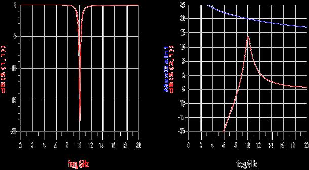
17 Match/Gain Plots MSG S11 S21
18 Comments on Design Input match looks good (S11 < 0.11) Power gain is as desired: G = 14 db Output match is terrible (S22 ~ 1) and close to instability! We see that this design requires some iteration to arrive at the best input/output match pair to give gain and good stability. In practice a lossy matching network (or added loss/ feedback to device) helps to create a good match.
Maxim > Design Support > Technical Documents > Application Notes > Wireless and RF > APP 1851
 Maxim > Design Support > Technical Documents > Application Notes > Wireless and RF > APP 1851 Keywords: lna, rf, rfic, amplifier, stability, power gain, transmission lines, rfics, theory, smith chart,
EECS 141: FALL 05 MIDTERM 1
 University of California College of Engineering Department of Electrical Engineering and Computer Sciences D. Markovic TuTh 11-1:3 Thursday, October 6, 6:3-8:pm EECS 141: FALL 5 MIDTERM 1 NAME Last SOLUTION
ECE-343 Test 2: Mar 21, :00-8:00, Closed Book. Name : SOLUTION
 ECE-343 Test 2: Mar 21, 2012 6:00-8:00, Closed Book Name : SOLUTION 1. (25 pts) (a) Draw a circuit diagram for a differential amplifier designed under the following constraints: Use only BJTs. (You may
Chapter 9 Frequency Response. PART C: High Frequency Response
 Chapter 9 Frequency Response PART C: High Frequency Response Discrete Common Source (CS) Amplifier Goal: find high cut-off frequency, f H 2 f H is dependent on internal capacitances V o Load Resistance
Circuit Topologies & Analysis Techniques in HF ICs
 Circuit Topologies & Analysis Techniques in HF ICs 1 Outline Analog vs. Microwave Circuit Design Impedance matching Tuned circuit topologies Techniques to maximize bandwidth Challenges in differential
EE105 Fall 2015 Microelectronic Devices and Circuits Frequency Response. Prof. Ming C. Wu 511 Sutardja Dai Hall (SDH)
") EE05 Fall 205 Microelectronic Devices and Circuits Frequency Response Prof. Ming C. Wu wu@eecs.berkeley.edu 5 Sutardja Dai Hall (SDH) Amplifier Frequency Response: Lower and Upper Cutoff Frequency Midband
EE05 Fall 205 Microelectronic Devices and Circuits Frequency Response Prof. Ming C. Wu wu@eecs.berkeley.edu 5 Sutardja Dai Hall (SDH) Amplifier Frequency Response: Lower and Upper Cutoff Frequency Midband
ECE-342 Test 3: Nov 30, :00-8:00, Closed Book. Name : Solution
 ECE-342 Test 3: Nov 30, 2010 6:00-8:00, Closed Book Name : Solution All solutions must provide units as appropriate. Unless otherwise stated, assume T = 300 K. 1. (25 pts) Consider the amplifier shown
CE/CS Amplifier Response at High Frequencies
 .. CE/CS Amplifier Response at High Frequencies INEL 4202 - Manuel Toledo August 20, 2012 INEL 4202 - Manuel Toledo CE/CS High Frequency Analysis 1/ 24 Outline.1 High Frequency Models.2 Simplified Method.3
ECE-343 Test 1: Feb 10, :00-8:00pm, Closed Book. Name : SOLUTION
 ECE-343 Test : Feb 0, 00 6:00-8:00pm, Closed Book Name : SOLUTION C Depl = C J0 + V R /V o ) m C Diff = τ F g m ω T = g m C µ + C π ω T = g m I / D C GD + C or V OV GS b = τ i τ i = R i C i ω H b Z = Z
ECE 415/515 ANALOG INTEGRATED CIRCUIT DESIGN
 ECE 415/515 ANALOG INTEGRATED CIRCUIT DESIGN CMOS PROCESS CHARACTERIZATION VISHAL SAXENA VSAXENA@UIDAHO.EDU Vishal Saxena DESIGN PARAMETERS Analog circuit designers care about: Open-loop Gain: g m r o
6.012 Electronic Devices and Circuits Spring 2005
 6.012 Electronic Devices and Circuits Spring 2005 May 16, 2005 Final Exam (200 points) -OPEN BOOK- Problem NAME RECITATION TIME 1 2 3 4 5 Total General guidelines (please read carefully before starting):
Lecture 23 Frequency Response of Amplifiers (I) Common Source Amplifier. December 1, 2005
 Common Source Amplifier. December 1, 2005") 6.02 Microelectronic Devices and Circuits Fall 2005 Lecture 23 Lecture 23 Frequency Response of Amplifiers (I) Common Source Amplifier December, 2005 Contents:. Introduction 2. Intrinsic frequency response
6.02 Microelectronic Devices and Circuits Fall 2005 Lecture 23 Lecture 23 Frequency Response of Amplifiers (I) Common Source Amplifier December, 2005 Contents:. Introduction 2. Intrinsic frequency response
Solutions to Problems in Chapter 5
 Appendix E Solutions to Problems in Chapter 5 E. Problem 5. Properties of the two-port network The network is mismatched at both ports (s 0 and s 0). The network is reciprocal (s s ). The network is symmetrical
EE C245 ME C218 Introduction to MEMS Design Fall 2011
 EE C245 ME C218 Introduction to MEMS Design Fall 2011 Prof. Clark T.-C. Nguyen Dept. of Electrical Engineering & Computer Sciences University of California at Berkeley Berkeley, CA 94720 Lecture EE C245:
EE 466/586 VLSI Design. Partha Pande School of EECS Washington State University
 EE 466/586 VLSI Design Partha Pande School of EECS Washington State University pande@eecs.wsu.edu Lecture 9 Propagation delay Power and delay Tradeoffs Follow board notes Propagation Delay Switching Time
General Topology of a single stage microwave amplifier
 General Topology of a ingle tage microwave amplifier Tak of MATCH network (in and out): To preent at the active device uitable impedance Z and Z S Deign Step The deign of a mall ignal microwave amplifier
Frequency Response Prof. Ali M. Niknejad Prof. Rikky Muller
 EECS 105 Spring 2017, Module 4 Frequency Response Prof. Ali M. Niknejad Department of EECS Announcements l HW9 due on Friday 2 Review: CD with Current Mirror 3 Review: CD with Current Mirror 4 Review:
ECE 391 supplemental notes - #11. Adding a Lumped Series Element
 ECE 391 supplemental notes - #11 Adding a umped Series Element Consider the following T-line circuit: Z R,1! Z,2! Z z in,1 = r in,1 + jx in,1 Z in,1 = z in,1 Z,1 z = Z Z,2 zin,2 = r in,2 + jx in,2 z,1
Lecture 37: Frequency response. Context
 EECS 05 Spring 004, Lecture 37 Lecture 37: Frequency response Prof J. S. Smith EECS 05 Spring 004, Lecture 37 Context We will figure out more of the design parameters for the amplifier we looked at in
CMOS Analog Circuits
 CMOS Analog Circuits L6: Common Source Amplifier-1 (.8.13) B. Mazhari Dept. of EE, IIT Kanpur 19 Problem statement : Design an amplifier which has the following characteristics: + CC O in R L - CC A 100
Measurement of S-Parameters. Transfer of the Reference Plane. Power Waves. Graphic Representation of Waves in Circuits
 Lecture 6 RF Amplifier Design Johan Wernehag Electrical and Information Technology Lecture 6 Amplifier Design Toughest week in the course, hang S-Parameters in there Definitions Power Waves Applications
3. Basic building blocks. Analog Design for CMOS VLSI Systems Franco Maloberti
 Inverter with active load It is the simplest gain stage. The dc gain is given by the slope of the transfer characteristics. Small signal analysis C = C gs + C gs,ov C 2 = C gd + C gd,ov + C 3 = C db +
Lecture 7: Transistors and Amplifiers
 Lecture 7: Transistors and Amplifiers Hybrid Transistor Model for small AC : The previous model for a transistor used one parameter (β, the current gain) to describe the transistor. doesn't explain many
UNIVERSITY OF CALIFORNIA College of Engineering Department of Electrical Engineering and Computer Sciences
 UNIVERSITY OF CALIFORNIA College of Engineering Department of Electrical Engineering and Computer Sciences E. Alon Final EECS 240 Monday, May 19, 2008 SPRING 2008 You should write your results on the exam
ECE 438: Digital Integrated Circuits Assignment #4 Solution The Inverter
 ECE 438: Digital Integrated Circuits Assignment #4 The Inverter Text: Chapter 5, Digital Integrated Circuits 2 nd Ed, Rabaey 1) Consider the CMOS inverter circuit in Figure P1 with the following parameters.
EE Power Gain and Amplifier Design 10/31/2017
 EE 40458 Power Gain and Amplifier Design 10/31/017 Motivation Brief recap: We ve studied matching networks (several types, how to design them, bandwidth, how they work, etc ) Studied network analysis techniques
1/13/12 V DS. I d V GS. C ox ( = f (V GS ,V DS ,V SB = I D. + i d + I ΔV + I ΔV BS V BS. 19 January 2012
 /3/ 9 January 0 Study the linear model of MOS transistor around an operating point." MOS in saturation: V GS >V th and V S >V GS -V th " VGS vi - I d = I i d VS I d = µ n ( L V V γ Φ V Φ GS th0 F SB F
ECE 546 Lecture 11 MOS Amplifiers
 ECE 546 Lecture MOS Amplifiers Spring 208 Jose E. Schutt-Aine Electrical & Computer Engineering University of Illinois jesa@illinois.edu ECE 546 Jose Schutt Aine Amplifiers Definitions Used to increase
Electronic Circuits Summary
 Electronic Circuits Summary Andreas Biri, D-ITET 6.06.4 Constants (@300K) ε 0 = 8.854 0 F m m 0 = 9. 0 3 kg k =.38 0 3 J K = 8.67 0 5 ev/k kt q = 0.059 V, q kt = 38.6, kt = 5.9 mev V Small Signal Equivalent
55:041 Electronic Circuits The University of Iowa Fall Final Exam
 Final Exam Name: Score Max: 135 Question 1 (1 point unless otherwise noted) a. What is the maximum theoretical efficiency for a class-b amplifier? Answer: 78% b. The abbreviation/term ESR is often encountered
Assignment 3 ELEC 312/Winter 12 R.Raut, Ph.D.
 Page 1 of 3 ELEC 312: ELECTRONICS II : ASSIGNMENT-3 Department of Electrical and Computer Engineering Winter 2012 1. A common-emitter amplifier that can be represented by the following equivalent circuit,
EE C245 ME C218 Introduction to MEMS Design
 EE C45 ME C8 Introduction to MEMS Design Fall 007 Prof. Clark T.-C. Nguyen Dept. of Electrical Engineering & Computer Sciences University of California at Berkeley Berkeley, CA 9470 Lecture 5: Output t
Advanced Current Mirrors and Opamps
 Advanced Current Mirrors and Opamps David Johns and Ken Martin (johns@eecg.toronto.edu) (martin@eecg.toronto.edu) slide 1 of 26 Wide-Swing Current Mirrors I bias I V I in out out = I in V W L bias ------------
6.301 Solid-State Circuits Recitation 14: Op-Amps and Assorted Other Topics Prof. Joel L. Dawson
 First, let s take a moment to further explore device matching for current mirrors: I R I 0 Q 1 Q 2 and ask what happens when Q 1 and Q 2 operate at different temperatures. It turns out that grinding through
Conventional Paper-I Part A. 1. (a) Define intrinsic wave impedance for a medium and derive the equation for intrinsic vy
 Define intrinsic wave impedance for a medium and derive the equation for intrinsic vy") EE-Conventional Paper-I IES-01 www.gateforum.com Conventional Paper-I-01 Part A 1. (a) Define intrinsic wave impedance for a medium and derive the equation for intrinsic vy impedance for a lossy dielectric
EE-Conventional Paper-I IES-01 www.gateforum.com Conventional Paper-I-01 Part A 1. (a) Define intrinsic wave impedance for a medium and derive the equation for intrinsic vy impedance for a lossy dielectric
Electronics II. Final Examination
 The University of Toledo f17fs_elct27.fm 1 Electronics II Final Examination Problems Points 1. 11 2. 14 3. 15 Total 40 Was the exam fair? yes no The University of Toledo f17fs_elct27.fm 2 Problem 1 11
Maximum Achievable Gain of a Two Port Network
 Maximum Achievable Gain of a Two Port Network Ali Niknejad Siva Thyagarajan Electrical Engineering and Computer Sciences University of California at Berkeley Technical Report No. UCB/EECS-2016-15 http://www.eecs.berkeley.edu/pubs/techrpts/2016/eecs-2016-15.html
Bipolar junction transistors
 Bipolar junction transistors Find parameters of te BJT in CE configuration at BQ 40 µa and CBQ V. nput caracteristic B / µa 40 0 00 80 60 40 0 0 0, 0,5 0,3 0,35 0,4 BE / V Output caracteristics C / ma
DESIGN MICROELECTRONICS ELCT 703 (W17) LECTURE 3: OP-AMP CMOS CIRCUIT. Dr. Eman Azab Assistant Professor Office: C
 LECTURE 3: OP-AMP CMOS CIRCUIT. Dr. Eman Azab Assistant Professor Office: C") MICROELECTRONICS ELCT 703 (W17) LECTURE 3: OP-AMP CMOS CIRCUIT DESIGN Dr. Eman Azab Assistant Professor Office: C3.315 E-mail: eman.azab@guc.edu.eg 1 TWO STAGE CMOS OP-AMP It consists of two stages: First
MICROELECTRONICS ELCT 703 (W17) LECTURE 3: OP-AMP CMOS CIRCUIT DESIGN Dr. Eman Azab Assistant Professor Office: C3.315 E-mail: eman.azab@guc.edu.eg 1 TWO STAGE CMOS OP-AMP It consists of two stages: First
ESE319 Introduction to Microelectronics. Feedback Basics
 Feedback Basics Stability Feedback concept Feedback in emitter follower One-pole feedback and root locus Frequency dependent feedback and root locus Gain and phase margins Conditions for closed loop stability
Stability & Compensation
 Advanced Analog Building Blocks Stability & Compensation Wei SHEN (KIP) 1 Bode Plot real zeros zeros with complex conjugates real poles poles with complex conjugates http://lpsa.swarthmore.edu/bode/bode.html
Chapter 10 Feedback. PART C: Stability and Compensation
 1 Chapter 10 Feedback PART C: Stability and Compensation Example: Non-inverting Amplifier We are analyzing the two circuits (nmos diff pair or pmos diff pair) to realize this symbol: either of the circuits
ECE 202 Fall 2013 Final Exam
 ECE 202 Fall 2013 Final Exam December 12, 2013 Circle your division: Division 0101: Furgason (8:30 am) Division 0201: Bermel (9:30 am) Name (Last, First) Purdue ID # There are 18 multiple choice problems
Metal-Oxide-Semiconductor Field Effect Transistor (MOSFET)
") Metal-Oxide-Semiconductor ield Effect Transistor (MOSET) Source Gate Drain p p n- substrate - SUB MOSET is a symmetrical device in the most general case (for example, in an integrating circuit) In a separate
Metal-Oxide-Semiconductor ield Effect Transistor (MOSET) Source Gate Drain p p n- substrate - SUB MOSET is a symmetrical device in the most general case (for example, in an integrating circuit) In a separate
Integrated Circuit Operational Amplifiers
 Analog Integrated Circuit Design A video course under the NPTEL Department of Electrical Engineering Indian Institute of Technology, Madras Chennai, 600036, India National Programme on Technology Enhanced
The Inverter. Digital Integrated Circuits A Design Perspective. Jan M. Rabaey Anantha Chandrakasan Borivoje Nikolic
 Digital Integrated Circuits A Design Perspective Jan M. Rabaey Anantha Chandrakasan Borivoje Nikolic The Inverter Revised from Digital Integrated Circuits, Jan M. Rabaey el, 2003 Propagation Delay CMOS
Lecture 23 - Frequency Resp onse of Amplifiers (I) Common-Source Amplifier. May 6, 2003
 Common-Source Amplifier. May 6, 2003") 6.0 Microelectronic Devices and Circuits Spring 003 Lecture 3 Lecture 3 Frequency Resp onse of Amplifiers (I) CommonSource Amplifier May 6, 003 Contents:. Intro duction. Intrinsic frequency resp onse of
6.0 Microelectronic Devices and Circuits Spring 003 Lecture 3 Lecture 3 Frequency Resp onse of Amplifiers (I) CommonSource Amplifier May 6, 003 Contents:. Intro duction. Intrinsic frequency resp onse of
Final Exam. 55:041 Electronic Circuits. The University of Iowa. Fall 2013.
 Final Exam Name: Max: 130 Points Question 1 In the circuit shown, the op-amp is ideal, except for an input bias current I b = 1 na. Further, R F = 10K, R 1 = 100 Ω and C = 1 μf. The switch is opened at
Lecture 7: Two-Ports (2)
") Lecture 7: Two-Ports (2) Amin Arbabian Jan M. Rabaey EE142 Fall 2010 Sept. 16 th, 2010 Announcements HW3 Posted, due Thursday September 23 rd, 330pm EE142 drop box. Office hours Two-Port notes by Professor
Lecture 7: Two-Ports (2) Amin Arbabian Jan M. Rabaey EE142 Fall 2010 Sept. 16 th, 2010 Announcements HW3 Posted, due Thursday September 23 rd, 330pm EE142 drop box. Office hours Two-Port notes by Professor
Gain Bandwidth Limitations of Microwave Transistor
 Gain Bandwidth Limitations of Microwave Transistor Filiz Güneş 1 Cemal Tepe 2 1 Department of Electronic and Communication Engineering, Yıldız Technical University, Beşiktaş 80750, Istanbul, Turkey 2 Alcatel,
Case Study: Parallel Coupled- Line Combline Filter
 MICROWAVE AND RF DESIGN MICROWAVE AND RF DESIGN Case Study: Parallel Coupled- Line Combline Filter Presented by Michael Steer Reading: 6. 6.4 Index: CS_PCL_Filter Based on material in Microwave and RF
University of Toronto. Final Exam
 University of Toronto Final Exam Date - Dec 16, 013 Duration:.5 hrs ECE331 Electronic Circuits Lecturer - D. Johns ANSWER QUESTIONS ON THESE SHEETS USING BACKS IF NECESSARY 1. Equation sheet is on last
ECE137B Final Exam. Wednesday 6/8/2016, 7:30-10:30PM.
 ECE137B Final Exam Wednesday 6/8/2016, 7:30-10:30PM. There are7 problems on this exam and you have 3 hours There are pages 1-32 in the exam: please make sure all are there. Do not open this exam until
Scattering Parameters
 Berkeley Scattering Parameters Prof. Ali M. Niknejad U.C. Berkeley Copyright c 2016 by Ali M. Niknejad September 7, 2017 1 / 57 Scattering Parameters 2 / 57 Scattering Matrix Voltages and currents are
Exact Analysis of a Common-Source MOSFET Amplifier
 Exact Analysis of a Common-Source MOSFET Amplifier Consider the common-source MOSFET amplifier driven from signal source v s with Thévenin equivalent resistance R S and a load consisting of a parallel
Sample-and-Holds David Johns and Ken Martin University of Toronto
 Sample-and-Holds David Johns and Ken Martin (johns@eecg.toronto.edu) (martin@eecg.toronto.edu) slide 1 of 18 Sample-and-Hold Circuits Also called track-and-hold circuits Often needed in A/D converters
Lecture 090 Multiple Stage Frequency Response - I (1/17/02) Page 090-1
 Page 090-1") Lecture 9 Multiple Stage Frequency esponse I (/7/2) Page 9 LECTUE 9 MULTIPLESTAGE FEQUENCY ESPONSE I (EADING: GHLM 56527) Objective The objective of this presentation is:.) Develop methods for the frequency
Lecture 9 Multiple Stage Frequency esponse I (/7/2) Page 9 LECTUE 9 MULTIPLESTAGE FEQUENCY ESPONSE I (EADING: GHLM 56527) Objective The objective of this presentation is:.) Develop methods for the frequency
Digital Integrated Circuits
 Chapter 6 The CMOS Inverter 1 Contents Introduction (MOST models) 0, 1 st, 2 nd order The CMOS inverter : The static behavior: o DC transfer characteristics, o Short-circuit current The CMOS inverter :
EE 240B Spring Advanced Analog Integrated Circuits Lecture 2: MOS Transistor Models. Elad Alon Dept. of EECS
 EE 240B Spring 2018 Advanced Analog Integrated Circuits Lecture 2: MOS Transistor Models Elad Alon Dept. of EECS Square Law Model? Assumptions made to come up with this model: Charge density determined
DC and Transient Responses (i.e. delay) (some comments on power too!)
 (some comments on power too!)") DC and Transient Responses (i.e. delay) (some comments on power too!) Michael Niemier (Some slides based on lecture notes by David Harris) 1 Lecture 02 - CMOS Transistor Theory & the Effects of Scaling
DC and Transient Responses (i.e. delay) (some comments on power too!) Michael Niemier (Some slides based on lecture notes by David Harris) 1 Lecture 02 - CMOS Transistor Theory & the Effects of Scaling
ECE 6412, Spring Final Exam Page 1 FINAL EXAMINATION NAME SCORE /120
 ECE 6412, Spring 2002 Final Exam Page 1 FINAL EXAMINATION NAME SCORE /120 Problem 1O 2O 3 4 5 6 7 8 Score INSTRUCTIONS: This exam is closed book with four sheets of notes permitted. The exam consists of
Stability and Frequency Compensation
 類比電路設計 (3349) - 2004 Stability and Frequency ompensation hing-yuan Yang National hung-hsing University Department of Electrical Engineering Overview Reading B Razavi hapter 0 Introduction In this lecture,
Two-Port Noise Analysis
 Berkeley Two-Port Noise Analysis Prof. Ali M. Niknejad U.C. Berkeley Copyright c 2015 by Ali M. Niknejad 1/26 Equivalent Noise Generators v 2 n Noisy Two-Port i 2 n Noiseless Two-Port Any noisy two port
Contents. Transmission Lines The Smith Chart Vector Network Analyser (VNA) ü structure ü calibration ü operation. Measurements
 ü structure ü calibration ü operation. Measurements") Contents Transmission Lines The Smith Chart Vector Network Analyser (VNA) ü structure ü calibration ü operation Measurements Göran Jönsson, EIT 2015-04-27 Vector Network Analysis 2 Waves on Lines If the
Contents Transmission Lines The Smith Chart Vector Network Analyser (VNA) ü structure ü calibration ü operation Measurements Göran Jönsson, EIT 2015-04-27 Vector Network Analysis 2 Waves on Lines If the
Studio 9 Review Operational Amplifier Stability Compensation Miller Effect Phase Margin Unity Gain Frequency Slew Rate Limiting Reading: Text sec 5.
 Studio 9 Review Operational Amplifier Stability Compensation Miller Effect Phase Margin Unity Gain Frequency Slew Rate Limiting Reading: Text sec 5.2 pp. 232-242 Two-stage op-amp Analysis Strategy Recognize
Transmission Lines. Plane wave propagating in air Y unguided wave propagation. Transmission lines / waveguides Y. guided wave propagation
 Transmission Lines Transmission lines and waveguides may be defined as devices used to guide energy from one point to another (from a source to a load). Transmission lines can consist of a set of conductors,
Common Drain Stage (Source Follower) Claudio Talarico, Gonzaga University
 Claudio Talarico, Gonzaga University") Common Drain Stage (Source Follower) Claudio Talarico, Gonzaga University Common Drain Stage v gs v i - v o V DD v bs - v o R S Vv IN i v i G C gd C+C gd gb B&D v s vv OUT o + V S I B R L C L v gs - C
Common Drain Stage (Source Follower) Claudio Talarico, Gonzaga University Common Drain Stage v gs v i - v o V DD v bs - v o R S Vv IN i v i G C gd C+C gd gb B&D v s vv OUT o + V S I B R L C L v gs - C
6.776 High Speed Communication Circuits Lecture 10 Noise Modeling in Amplifiers
 6.776 High Speed Communication Circuits Lecture 10 Noise Modeling in Amplifiers Michael Perrott Massachusetts Institute of Technology March 8, 2005 Copyright 2005 by Michael H. Perrott Notation for Mean,
Microelectronic Circuit Design 4th Edition Errata - Updated 4/4/14
 Chapter Text # Inside back cover: Triode region equation should not be squared! i D = K n v GS "V TN " v & DS % ( v DS $ 2 ' Page 49, first exercise, second answer: -1.35 x 10 6 cm/s Page 58, last exercise,
The transistor is not in the cutoff region. the transistor is in the saturation region. To see this, recognize that in a long-channel transistor ifv
 ECE 440 Spring 005 Page 1 Homework Assignment No. Solutions P.4 For each transistor, first determine if the transistor is in cutoff by checking to see if GS is less than or greater than. may have to be
ECE137B Final Exam. There are 5 problems on this exam and you have 3 hours There are pages 1-19 in the exam: please make sure all are there.
 ECE37B Final Exam There are 5 problems on this exam and you have 3 hours There are pages -9 in the exam: please make sure all are there. Do not open this exam until told to do so Show all work: Credit
Application Report. Mixed Signal Products SLOA021
 Application Report May 1999 Mixed Signal Products SLOA021 IMPORTANT NOTICE Texas Instruments and its subsidiaries (TI) reserve the right to make changes to their products or to discontinue any product
Practice 7: CMOS Capacitance
 Practice 7: CMOS Capacitance Digital Electronic Circuits Semester A 2012 MOSFET Capacitances MOSFET Capacitance Components 3 Gate to Channel Capacitance In general, the gate capacitance is similar to a
Lecture 050 Followers (1/11/04) Page ECE Analog Integrated Circuits and Systems II P.E. Allen
 Page ECE Analog Integrated Circuits and Systems II P.E. Allen") Lecture 5 Followers (1/11/4) Page 51 LECTURE 5 FOLLOWERS (READING: GHLM 344362, AH 221226) Objective The objective of this presentation is: Show how to design stages that 1.) Provide sufficient output
Lecture 5 Followers (1/11/4) Page 51 LECTURE 5 FOLLOWERS (READING: GHLM 344362, AH 221226) Objective The objective of this presentation is: Show how to design stages that 1.) Provide sufficient output
Class E Design Formulas V DD
 Class E Design Formulas V DD RFC C L+X/ω V s (θ) I s (θ) Cd R useful functions and identities Units Constants Table of Contents I. Introduction II. Process Parameters III. Inputs IV. Standard Class E Design
EECS 105: FALL 06 FINAL
 University of California College of Engineering Department of Electrical Engineering and Computer Sciences Jan M. Rabaey TuTh 2-3:30 Wednesday December 13, 12:30-3:30pm EECS 105: FALL 06 FINAL NAME Last
TPC8116-H TPC8116-H. High Efficiency DC/DC Converter Applications Notebook PC Applications Portable Equipment Applications CCFL Inverter Applications
 TOSHIBA Field Effect Transistor Silicon P-Channel MOS Type (Ultra-High-Speed U-MOSIII) High Efficiency DC/DC Converter Applications Notebook PC Applications Portable Equipment Applications CCFL Inverter
Homework Assignment 08
 Homework Assignment 08 Question 1 (Short Takes) Two points each unless otherwise indicated. 1. Give one phrase/sentence that describes the primary advantage of an active load. Answer: Large effective resistance
V DD. M 1 M 2 V i2. V o2 R 1 R 2 C C
 UNVERSTY OF CALFORNA Collee of Enineerin Department of Electrical Enineerin and Computer Sciences E. Alon Homework #3 Solutions EECS 40 P. Nuzzo Use the EECS40 90nm CMOS process in all home works and projects
Hw 6 and 7 Graded and available Project Phase 2 Graded Project Phase 3 Launch Today
 EECS141 1 Hw 8 Posted Last one to be graded Due Friday April 30 Hw 6 and 7 Graded and available Project Phase 2 Graded Project Phase 3 Launch Today EECS141 2 1 6 5 4 3 2 1 0 1.5 2 2.5 3 3.5 4 Frequency
EECE 301 Signals & Systems Prof. Mark Fowler
 EECE 3 Signals & Systems Prof. Mark Fowler Note Set #9 C-T Systems: Laplace Transform Transfer Function Reading Assignment: Section 6.5 of Kamen and Heck /7 Course Flow Diagram The arrows here show conceptual
Department of Electrical Engineering and Computer Sciences University of California, Berkeley. Final Exam: Friday, August 10, 2012
 Electrical Engineering 42/00 Summer 202 Instructor: Tony Dear Department of Electrical Engineering and Computer Sciences University of California, Berkeley Final Exam: Friday, August 0, 202 Last Name:
TRANSMISSION LINES AND MATCHING
 TRANSMISSION LINES AND MATCHING for High-Frequency Circuit Design Elective by Michael Tse September 2003 Contents Basic models The Telegrapher s equations and solutions Transmission line equations The
Preamplifier in 0.5µm CMOS
 A 2.125 Gbaud 1.6kΩ Transimpedance Preamplifier in 0.5µm CMOS Sunderarajan S. Mohan Thomas H. Lee Center for Integrated Systems Stanford University OUTLINE Motivation Shunt-peaked Amplifier Inductor Modeling
Power Management Circuits and Systems. Basic Concepts: Amplifiers and Feedback. Jose Silva-Martinez
 Power Management Circuits and Systems Basic Concepts: Amplifiers and Feedback Jose Silva-Martinez Department of Electrical & Computer Engineering Texas A&M University January 2, 209 Non-Inverting Amplifier
Next, we check the race condition to see if the circuit will work properly. Note that the minimum logic delay is a single sum.
 UNIVERSITY OF CALIFORNIA College of Engineering Department of Electrical Engineering and Computer Sciences Last modified on May 1, 2003 by Dejan Markovic (dejan@eecs.berkeley.edu) Prof. Jan Rabaey EECS
Lecture 14 Date:
 Lecture 14 Date: 18.09.2014 L Type Matching Network Examples Nodal Quality Factor T- and Pi- Matching Networks Microstrip Matching Networks Series- and Shunt-stub Matching L Type Matching Network (contd.)
and V DS V GS V T (the saturation region) I DS = k 2 (V GS V T )2 (1+ V DS )
 I DS = k 2 (V GS V T )2 (1+ V DS )") ECE 4420 Spring 2005 Page 1 FINAL EXAMINATION NAME SCORE /100 Problem 1O 2 3 4 5 6 7 Sum Points INSTRUCTIONS: This exam is closed book. You are permitted four sheets of notes (three of which are your sheets
ECE 4420 Spring 2005 Page 1 FINAL EXAMINATION NAME SCORE /100 Problem 1O 2 3 4 5 6 7 Sum Points INSTRUCTIONS: This exam is closed book. You are permitted four sheets of notes (three of which are your sheets
Workshop WMB. Noise Modeling
 Workshop WMB Noise Modeling Manfred Berroth, Markus Grözing, Stefan Heck, Alexander Bräckle University of Stuttgart, Germany WMB (IMS) Parameter Extraction Strategies For Compact Transistor Models IMS
Chapter 4 Field-Effect Transistors
 Chapter 4 Field-Effect Transistors Microelectronic Circuit Design Richard C. Jaeger Travis N. Blalock 5/5/11 Chap 4-1 Chapter Goals Describe operation of MOSFETs. Define FET characteristics in operation
Name. Section. Short Answer Questions. 1. (20 Pts) 2. (10 Pts) 3. (5 Pts) 4. (10 Pts) 5. (10 Pts) Regular Questions. 6. (25 Pts) 7.
 2. (10 Pts) 3. (5 Pts) 4. (10 Pts) 5. (10 Pts) Regular Questions. 6. (25 Pts) 7.") Name Section Short Answer Questions 1. (20 Pts) 2. (10 Pts) 3. (5 Pts). (10 Pts) 5. (10 Pts) Regular Questions 6. (25 Pts) 7. (20 Pts) Notes: 1. Please read over all questions before you begin your work.
Name Section Short Answer Questions 1. (20 Pts) 2. (10 Pts) 3. (5 Pts). (10 Pts) 5. (10 Pts) Regular Questions 6. (25 Pts) 7. (20 Pts) Notes: 1. Please read over all questions before you begin your work.
Maximum Ratings Parameter Symbol Value Unit Continuous drain current T C = 25 C T C = 100 C I D 20.7
 Cool MOS Power Transistor V DS @ T jmax 65 V Feature R DS(on).22 Ω New revolutionary high voltage technology Ultra low gate charge Periodic avalanche rated Extreme dv/dt rated High peak current capability
(Refer Slide Time: 1:49)
") Analog Electronic Circuits Professor S. C. Dutta Roy Department of Electrical Engineering Indian Institute of Technology Delhi Lecture no 14 Module no 01 Midband analysis of FET Amplifiers (Refer Slide
Analog Electronic Circuits Professor S. C. Dutta Roy Department of Electrical Engineering Indian Institute of Technology Delhi Lecture no 14 Module no 01 Midband analysis of FET Amplifiers (Refer Slide
Waves on Lines. Contents. ! Transmission Lines! The Smith Chart! Vector Network Analyser (VNA) ! Measurements
 ! Measurements") Waves on Lines If the wavelength to be considered is significantly greater compared to the size of the circuit the voltage will be independent of the location. amplitude d! distance but this is not true
Waves on Lines If the wavelength to be considered is significantly greater compared to the size of the circuit the voltage will be independent of the location. amplitude d! distance but this is not true
Feedback Transimpedance & Current Amplifiers
 Feedback Transimpedance & Current Amplifiers Willy Sansen KULeuven, ESATMICAS Leuven, Belgium willy.sansen@esat.kuleuven.be Willy Sansen 1005 141 Table of contents Introduction Shuntshunt FB for Transimpedance
Lecture 9. The Smith Chart and Basic Impedance-Matching Concepts
 ecture 9 The Smith Chart and Basic Impedance-Matching Concepts The Smith Chart: Γ plot in the Complex Plane Smith s chart is a graphical representation in the complex Γ plane of the input impedance, the
Circle the one best answer for each question. Five points per question.
 ID # NAME EE-255 EXAM 3 November 8, 2001 Instructor (circle one) Talavage Gray This exam consists of 16 multiple choice questions and one workout problem. Record all answers to the multiple choice questions
Module 2 : Transmission Lines. Lecture 10 : Transmisssion Line Calculations Using Smith Chart. Objectives. In this course you will learn the following
 Objectives In this course you will learn the following What is a constant VSWR circle on the - plane? Properties of constant VSWR circles. Calculations of load reflection coefficient. Calculation of reflection
Electronics II. Midterm #1
 The University of Toledo EECS:3400 Electronics I su3ms_elct7.fm Section Electronics II Midterm # Problems Points. 5. 6 3. 9 Total 0 Was the exam fair? yes no The University of Toledo su3ms_elct7.fm Problem
Impedance Matching and Tuning
 C h a p t e r F i v e Impedance Matching and Tuning This chapter marks a turning point, in that we now begin to apply the theory and techniques of previous chapters to practical problems in microwave engineering.