The Inverter. Digital Integrated Circuits A Design Perspective. Jan M. Rabaey Anantha Chandrakasan Borivoje Nikolic
|
|
|
- Johnathan Haynes
- 5 years ago
- Views:
Transcription

1 Digital Integrated Circuits A Design Perspective Jan M. Rabaey Anantha Chandrakasan Borivoje Nikolic The Inverter Revised from Digital Integrated Circuits, Jan M. Rabaey el, 2003
2 Propagation Delay
3 CMOS Inverter Propagation Delay V DD t phl = f(r on.c L ) = 0.69 R on C L V out V out ln(0.5) R on C L 1 V DD V in = V DD R on C L t
4 MOS transistor model for simulation G C GS C GD S D C SB C GB C DB B
5 Computing the Capacitances Consider each capacitor individually is almost impossible for manual analysis. What capacitors count in CL? V DD V DD M2 C db2 C g4 M4 V in C gd12 V out V out2 M1 C db1 C w C g3 M3 Interconnect Fanout Simplified Model V in V out C L
6 Computing the Capacitances NMOS and PMOS transistor are either in cutoff or saturation mode during at least the first half (50%) of the output transient. So, the only contributions to Cgd are the overlap capacitance, since channel capacitance occurs between either Gate-Body for transistors in cutoff region or Gate- Source for transistors in saturation region.
7 The Miller Effect The lumped capacitor model requires the floating Cgd1 capacitor be replaced by a capacitor to GND using Miller effect. V C gd1 V out V out V V in V 2C gd1 M1 V V in M1 A capacitor experiencing identical but opposite voltage swings at both its terminals can be replaced by a capacitor to ground, whose value is two times the original value.
 the top output terminal if an impedance Z out, Miller is connected across the output terminal This is know as Miller Effect Two")
8 The Miller Effect Consider the situation that an impedance is connected between input and output of an amplifier The same current flows from (out) the top input terminal if an impedance Z in, Miller is connected across the input terminals The same current flows to (in) the top output terminal if an impedance Z out, Miller is connected across the output terminal This is know as Miller Effect Two important notes to apply Miller Effect: There should be a common terminal for input and output The gain in the Miller Effect is the gain after connecting feedback impedance Z f Graphs from Prentice Hall
9 Computing the Capacitances The capacitance between drain and bulk, Cdb1 and Cdb2, are due to the reverse-biased pnjunction. Such a capacitor is, unfortunately, quite nonlinear and depends heavily on the applied voltage. In Chapter 3 we replaced the nonlinear capacitor by a linear one with the same change in charge for the voltage range of interest. A multiplication factor, Keq, is introduced to relate the linearized capacitor to the value of the junction capacitance under zero-bias conditions (usually in the range of 0.6 to 0.9).
10 Junction Capacitance
11 Linearizing the Junction Capacitance Replace non-linear capacitance by large-signal equivalent linear capacitance which displaces equal charge over voltage swing of interest


12 9λ/2λ PMOS V DD ADp=45 λ 2 PDp=19 λ In Polysilicon NMOS 3λ/2λ Out Metal1 GND ADn=19 λ 2 PDn=15 λ
13 Junction Capacitance Ls (from Ch. 3) Channel-stop implant N A Side wall W Source N D Bottom x j Side wall Channel L S Substrate N A Junction capacitance per unit length No channel side Junction capacitance per unit area
14 Computation of all capacitors Intrinsic extrinsic Cdb will be slightly different (the pn junction reverse bias in L-to-H and H-to-L, why? voltage range)
15 Transient Response Cgd directly couples the steep input change before the circuit can even start to react to the changes at input (potential forward bias the pn junction) 3 2.5? V out (V) t phl t plh t p = 0.69 C L (R eqn +R eqp )/ t (sec) x 10-10
16 Low-to-High and High-to-Low delay It is desired to have identical propagation delays for both rising and falling inputs. Equal delay requires equal equivalent onresistance, thus equal current IDAST (neglecting the channel length modulation) This demands almost the same requirements for a Vm at VDD/2. Why?
17 Requirements for equal delay I I I DSAT Dn Dp k k k ' n ' p ' W L W ( ) L W ( ) L ( V n p V V DD DSATn DSATp V T ( V ( V ) V DD DD DSAT V V V Tn Tp 2 DSAT 2 V ) V ) 2 2 DSATn DSATp Assume V then k k ' p ' n V V DD DSATp DSATn V ( W ( W Tp / L) / L) V p n DSATp k k p n / 2 V V DSATp DSATn 1 This is exactly the formerly defined parameter r (last lecture)
18 Design for delay performance Keep capacitances small careful layout, e.g. to keep drain diffusion as small as possible Increase transistor sizes watch out for self-loading! When intrinsic capacitance starts to dominate the extrinsic ones Increase VDD (????)
19 Delay as a function of V DD For fixed (W/L) t p (normalized) Recall a range of low voltage is able to give even better voltage transfer characteristic V DD (V)
20 Device Sizing 3.8 x (for fixed load and VDD) t p (sec) Self-loading effect: Intrinsic capacitances dominate W/L S
21 NMOS/PMOS ratio 5 x tplh tphl t p (sec) 4 (Average) tp b= W p /W n Lp=L n b Widening PMOS improves the L-H delay by increasing the charge current, but it also degrades the H-L by giving a larger parasitic capacitance. Considering average is more meaningful!!
22 Delay Definitions
23 Impact of Rise Time on Delay t phl (nsec) t rise (nsec) 0.8 1
24 Custom design process: An inverter design example
25 1. Schematic design

26 2. Layout design
27 Step 1: define Nwell (for PMOS)
28 Step 2: define pselect (for PMOS location)

29 Step 3: define active region (for PMOS)
30 Step 4: define poly (gate for PMOS)
31 Step 5: define contacts (for PMOS)
")
32 Step 6: define Vdd and connect source (of PMOS) to it
33 Step 7: make at least one Nwell contact
34 Step 8: create NMOS (repeat similar steps before except you do not need make Nwell)
35 step9: make input and output connections

36 2. DRC (Design Rule Check)
37 Correct error if there is any
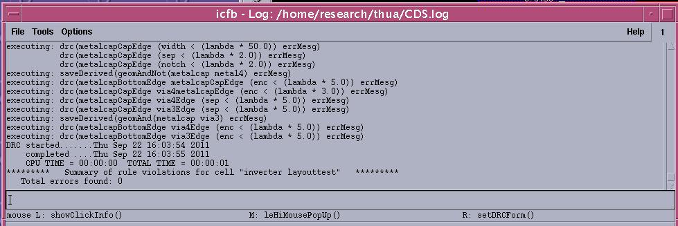
38 After correction

39 3. LVS (Layout versus Schematic)

40 4. Extract Layout parasitics and post-layout simulation

41 CMOS Inverter N Well V DD V DD PMOS 2l PMOS Contacts In Out In Out Metal 1 NMOS Polysilicon NMOS GND
42 Two Inverters Layout preference: Share power and ground Abut cells V DD Connect in Metal
43 Impact of Process Variations (DFM) 2.5 V out (V) Good NMOS Bad PMOS Nominal Good PMOS Bad NMOS V in (V)
44 Inverter Sizing for delay
45 Inverter with Load W means the size is increased by a factor of W with respect to the minimum size 3W Delay W C int C L Load Delay = kr W (C int + C L ) = kr W C int + kr W C L = Delay (Internal) + Delay (Load) = krw Cint(1+ CL /Cint)
46 Delay as function of size Delay = kr W C int (1+ C L /C int ) = Delay (Internal) + Delay (Load) RW = R unit / W ; C int = W C unit t p t (1 C /( WC p0 L unit )) t p0 = 0.69R unit C unit Intrinsic delay is fixed and independent of sizew Making W large yields better performance gain, eliminating the impact of external load and reducing the delay to intrinsic only. But smaller gain at penalty of silicon area if W is too large!
47 Delay Formula Delay ~ R W C int C L t p kr W C int 1 C / C t 1 f / L int p0 C int = C gin with 1 for modern technology (see page199 in book or Slid 14 for an example) Cgin : input gate capacitance C L = f C gin - effective fanout This formula maps the intrinsic capacitor and load capacitor as functions of a common capacitor, which is the gate capacitance of the minimum-size inverter
48 Single inverter versus inverter chain Gate sizing for an isolated gate is not really meaningful. Realistic chips always have a long chain of gates. So, a more relevant and realistic problem is to determine the optimal sizing for a chain of gates.
49 Inverter Chain In Out C L If C L is given: - How many stages are needed to minimize the delay? - How to size the inverters?
50 Apply to Inverter Chain (fixed N stages) Unit size (minimum size) inverter In Size? Size? Out 1 2 N C L t p = t p1 + t p2 + + t pn t t pj p ~ R unit C unit 1 C gin, j1 C gin, j C 1 C N N gin j t p j t, 1, p0, C gin, N 1 j1 i1 gin, j C L
51 Optimal Tapering for Given N Delay equation has N - 1 unknowns, C gin,2 C gin,n Minimize the delay, find N - 1 partial derivatives equated to 0 Result: C gin,j+1 /C gin,j = C gin,j /C gin,j-1 Size of each stage is the geometric mean of two neighbors C gin, j gin, j1 gin, j1 - each stage has the same effective fanout - each stage has the same delay C C
52 Optimum Delay for fixed N stages When each stage is sized by f and has same effective fanout f: f N F C Effective fanout of each stage: L / Cgin,1 effective fanout of the overall circuit Minimum path delay t p N j1 t f N F C gin, j1 1 Nt p0(1 C gin j N N p, j t p0 F / i1, )
53 Example In C 1 1 f f 2 Out C L = 8 C 1 C L /C 1 has to be evenly distributed across N = 3 stages: f 3 8 2
54 Optimum Number of Stages For a given load C L and given input capacitance C in Find optimal sizing f t p C Nt L p0 t f t ln 1/ N p0 F / 1 p F C t p0 in ln f F N C ln in f with F 1 2 ln f N f ln f f ln ln F f 0 ln f For = 0, f = e, N = lnf f exp 1 f
55 Optimum Effective Fanout f Optimum f for given process defined by f 1 f exp f opt = 3.6 for =1
56 Impact of introducing buffers t p N Nt 1 F / f opt = 4 p0
57 Buffer Design N f t p
58 Intel Itanium Microprocessor 9-1 Mux 5-1 Mux a CARRYGEN g64 node1 ck1 SUMSEL REG sum sumb to Cache 9-1 Mux 2-1 Mux b SUMGEN + LU s0 s1 LU : Logical Unit 1000um Itanium has 6 integer execution units like this 58
The CMOS Inverter: A First Glance
 The CMOS Inverter: A First Glance V DD V in V out C L CMOS Properties Full rail-to-rail swing Symmetrical VTC Propagation delay function of load capacitance and resistance of transistors No static power
Chapter 5. The Inverter. V1. April 10, 03 V1.1 April 25, 03 V2.1 Nov Inverter
 Chapter 5 The Inverter V1. April 10, 03 V1.1 April 25, 03 V2.1 Nov.12 03 Objective of This Chapter Use Inverter to know basic CMOS Circuits Operations Watch for performance Index such as Speed (Delay calculation)
The CMOS Inverter: A First Glance
 The CMOS Inverter: A First Glance V DD S D V in V out C L D S CMOS Inverter N Well V DD V DD PMOS 2λ PMOS Contacts In Out In Out Metal 1 NMOS Polysilicon NMOS GND CMOS Inverter: Steady State Response V
Lecture 4: CMOS review & Dynamic Logic
 Lecture 4: CMOS review & Dynamic Logic Reading: ch5, ch6 Overview CMOS basics Power and energy in CMOS Dynamic logic 1 CMOS Properties Full rail-to-rail swing high noise margins Logic levels not dependent
Digital Integrated Circuits 2nd Inverter
 Digital Integrated Circuits The Inverter The CMOS Inverter V DD Analysis Inverter complex gate Cost V in V out complexity & Area Integrity and robustness C L Static behavior Performance Dynamic response
Check course home page periodically for announcements. Homework 2 is due TODAY by 5pm In 240 Cory
 EE141 Fall 005 Lecture 6 MOS Capacitances, Propagation elay Important! Check course home page periodically for announcements Homework is due TOAY by 5pm In 40 Cory Homework 3 will be posted TOAY ue Thursday
Integrated Circuits & Systems
 Federal University of Santa Catarina Center for Technology Computer Science & Electronics Engineering Integrated Circuits & Systems INE 5442 Lecture 14 The CMOS Inverter: dynamic behavior (sizing, inverter
Announcements. EE141- Fall 2002 Lecture 7. MOS Capacitances Inverter Delay Power
 - Fall 2002 Lecture 7 MOS Capacitances Inverter Delay Power Announcements Wednesday 12-3pm lab cancelled Lab 4 this week Homework 2 due today at 5pm Homework 3 posted tonight Today s lecture MOS capacitances
5.0 CMOS Inverter. W.Kucewicz VLSICirciuit Design 1
 5.0 CMOS Inverter W.Kucewicz VLSICirciuit Design 1 Properties Switching Threshold Dynamic Behaviour Capacitance Propagation Delay nmos/pmos Ratio Power Consumption Contents W.Kucewicz VLSICirciuit Design
COMP 103. Lecture 10. Inverter Dynamics: The Quest for Performance. Section 5.4.2, What is this lecture+ about? PERFORMANCE
 COMP 103 Lecture 10 Inverter Dynamics: The Quest for Performance Section 5.4.2, 5.4.3 [All lecture notes are adapted from Mary Jane Irwin, Penn State, which were adapted from Rabaey s Digital Integrated
THE INVERTER. Inverter
 THE INVERTER DIGITAL GATES Fundamental Parameters Functionality Reliability, Robustness Area Performance» Speed (delay)» Power Consumption» Energy Noise in Digital Integrated Circuits v(t) V DD i(t) (a)
CMPEN 411 VLSI Digital Circuits. Lecture 04: CMOS Inverter (static view)
") CMPEN 411 VLSI Digital Circuits Lecture 04: CMOS Inverter (static view) Kyusun Choi [Adapted from Rabaey s Digital Integrated Circuits, Second Edition, 2003 J. Rabaey, A. Chandrakasan, B. Nikolic] CMPEN
CMPEN 411 VLSI Digital Circuits Lecture 04: CMOS Inverter (static view) Kyusun Choi [Adapted from Rabaey s Digital Integrated Circuits, Second Edition, 2003 J. Rabaey, A. Chandrakasan, B. Nikolic] CMPEN
CMOS Inverter (static view)
") Review: Design Abstraction Levels SYSTEM CMOS Inverter (static view) + MODULE GATE [Adapted from Chapter 5. 5.3 CIRCUIT of G DEVICE Rabaey s Digital Integrated Circuits,, J. Rabaey et al.] S D Review:
Review: Design Abstraction Levels SYSTEM CMOS Inverter (static view) + MODULE GATE [Adapted from Chapter 5. 5.3 CIRCUIT of G DEVICE Rabaey s Digital Integrated Circuits,, J. Rabaey et al.] S D Review:
Announcements. EE141- Spring 2003 Lecture 8. Power Inverter Chain
 - Spring 2003 Lecture 8 Power Inverter Chain Announcements Homework 3 due today. Homework 4 will be posted later today. Special office hours from :30-3pm at BWRC (in lieu of Tuesday) Today s lecture Power
The Devices. Digital Integrated Circuits A Design Perspective. Jan M. Rabaey Anantha Chandrakasan Borivoje Nikolic. July 30, 2002
 Digital Integrated Circuits A Design Perspective Jan M. Rabaey Anantha Chandrakasan Borivoje Nikolic The Devices July 30, 2002 Goal of this chapter Present intuitive understanding of device operation Introduction
ENGR890 Digital VLSI Design Fall Lecture 4: CMOS Inverter (static view)
") ENGR89 Digital VLSI Design Fall 5 Lecture 4: CMOS Inverter (static view) [Adapted from Chapter 5 of Digital Integrated Circuits, 3, J. Rabaey et al.] [Also borrowed from Vijay Narayanan and Mary Jane Irwin]
ENGR89 Digital VLSI Design Fall 5 Lecture 4: CMOS Inverter (static view) [Adapted from Chapter 5 of Digital Integrated Circuits, 3, J. Rabaey et al.] [Also borrowed from Vijay Narayanan and Mary Jane Irwin]
The Physical Structure (NMOS)
") The Physical Structure (NMOS) Al SiO2 Field Oxide Gate oxide S n+ Polysilicon Gate Al SiO2 SiO2 D n+ L channel P Substrate Field Oxide contact Metal (S) n+ (G) L W n+ (D) Poly 1 Transistor Resistance Two
The Physical Structure (NMOS) Al SiO2 Field Oxide Gate oxide S n+ Polysilicon Gate Al SiO2 SiO2 D n+ L channel P Substrate Field Oxide contact Metal (S) n+ (G) L W n+ (D) Poly 1 Transistor Resistance Two
CMPEN 411 VLSI Digital Circuits Spring 2012
 CMPEN 411 VLSI Digital Circuits Spring 2012 Lecture 09: Resistance & Inverter Dynamic View [Adapted from Rabaey s Digital Integrated Circuits, Second Edition, 2003 J. Rabaey, A. Chandrakasan, B. Nikolic]
MOSFET: Introduction
 E&CE 437 Integrated VLSI Systems MOS Transistor 1 of 30 MOSFET: Introduction Metal oxide semiconductor field effect transistor (MOSFET) or MOS is widely used for implementing digital designs Its major
Today s lecture. EE141- Spring 2003 Lecture 4. Design Rules CMOS Inverter MOS Transistor Model
 - Spring 003 Lecture 4 Design Rules CMOS Inverter MOS Transistor Model Today s lecture Design Rules The CMOS inverter at a glance An MOS transistor model for manual analysis Important! Labs start next
Lecture 4: CMOS Transistor Theory
 Introduction to CMOS VLSI Design Lecture 4: CMOS Transistor Theory David Harris, Harvey Mudd College Kartik Mohanram and Steven Levitan University of Pittsburgh Outline q Introduction q MOS Capacitor q
EE5311- Digital IC Design
 EE5311- Digital IC Design Module 3 - The Inverter Janakiraman V Assistant Professor Department of Electrical Engineering Indian Institute of Technology Madras Chennai September 3, 2018 Janakiraman, IITM
Integrated Circuits & Systems
 Federal University of Santa Catarina Center for Technology Computer Science & Electronics Engineering Integrated Circuits & Systems INE 5442 Lecture 13 The CMOS Inverter: dynamic behavior (delay) guntzel@inf.ufsc.br
ECE 438: Digital Integrated Circuits Assignment #4 Solution The Inverter
 ECE 438: Digital Integrated Circuits Assignment #4 The Inverter Text: Chapter 5, Digital Integrated Circuits 2 nd Ed, Rabaey 1) Consider the CMOS inverter circuit in Figure P1 with the following parameters.
Dynamic operation 20
 Dynamic operation 20 A simple model for the propagation delay Symmetric inverter (rise and fall delays are identical) otal capacitance is linear t p Minimum length devices R W C L t = 0.69R C = p W L 0.69
ENEE 359a Digital VLSI Design
 SLIDE 1 ENEE 359a Digital VLSI Design & Logical Effort Prof. blj@ece.umd.edu Credit where credit is due: Slides contain original artwork ( Jacob 2004) as well as material taken liberally from Irwin & Vijay
Integrated Circuits & Systems
 Federal University of Santa Catarina Center for Technology Computer Science & Electronics Engineering Integrated Circuits & Systems INE 5442 Lecture 12 The CMOS Inverter: static behavior guntzel@inf.ufsc.br
EECS 141: FALL 05 MIDTERM 1
 University of California College of Engineering Department of Electrical Engineering and Computer Sciences D. Markovic TuTh 11-1:3 Thursday, October 6, 6:3-8:pm EECS 141: FALL 5 MIDTERM 1 NAME Last SOLUTION
EE115C Winter 2017 Digital Electronic Circuits. Lecture 3: MOS RC Model, CMOS Manufacturing
 EE115C Winter 2017 Digital Electronic Circuits Lecture 3: MOS RC Model, CMOS Manufacturing Agenda MOS Transistor: RC Model (pp. 104-113) S R on D CMOS Manufacturing Process (pp. 36-46) S S C GS G G C GD
ECE321 Electronics I
 ECE31 Electronics Lecture 1: CMOS nverter: Noise Margin & Delay Model Payman Zarkesh-Ha Office: ECE Bldg. 30B Office hours: Tuesday :00-3:00PM or by appointment E-mail: payman@ece.unm.edu Slide: 1 CMOS
CMOS INVERTER. Last Lecture. Metrics for qualifying digital circuits. »Cost» Reliability» Speed (delay)»performance
»performance") CMOS INVERTER Last Lecture Metrics for qualifying digital circuits»cost» Reliability» Speed (delay)»performance 1 Today s lecture The CMOS inverter at a glance An MOS transistor model for manual analysis
CMOS INVERTER Last Lecture Metrics for qualifying digital circuits»cost» Reliability» Speed (delay)»performance 1 Today s lecture The CMOS inverter at a glance An MOS transistor model for manual analysis
The Devices. Digital Integrated Circuits A Design Perspective. Jan M. Rabaey Anantha Chandrakasan Borivoje Nikolic. July 30, 2002
 igital Integrated Circuits A esign Perspective Jan M. Rabaey Anantha Chandrakasan Borivoje Nikolic The evices July 30, 2002 Goal of this chapter Present intuitive understanding of device operation Introduction
Digital Integrated Circuits A Design Perspective. Arithmetic Circuits. Jan M. Rabaey Anantha Chandrakasan Borivoje Nikolic.
 Digital Integrated Circuits A Design Perspective Jan M. Rabaey Anantha Chandrakasan Borivoje Nikolic Arithmetic Circuits January, 2003 1 A Generic Digital Processor MEM ORY INPUT-OUTPUT CONTROL DATAPATH
Digital Microelectronic Circuits ( )
") Digital Microelectronic ircuits (361-1-3021 ) Presented by: Dr. Alex Fish Lecture 5: Parasitic apacitance and Driving a Load 1 Motivation Thus far, we have learned how to model our essential building block,
Digital Microelectronic ircuits (361-1-3021 ) Presented by: Dr. Alex Fish Lecture 5: Parasitic apacitance and Driving a Load 1 Motivation Thus far, we have learned how to model our essential building block,
EEC 118 Lecture #5: CMOS Inverter AC Characteristics. Rajeevan Amirtharajah University of California, Davis Jeff Parkhurst Intel Corporation
 EEC 8 Lecture #5: CMOS Inverter AC Characteristics Rajeevan Amirtharajah University of California, Davis Jeff Parkhurst Intel Corporation Acknowledgments Slides due to Rajit Manohar from ECE 547 Advanced
ECE 546 Lecture 10 MOS Transistors
 ECE 546 Lecture 10 MOS Transistors Spring 2018 Jose E. Schutt-Aine Electrical & Computer Engineering University of Illinois jesa@illinois.edu NMOS Transistor NMOS Transistor N-Channel MOSFET Built on p-type
MOS Transistor Theory
 MOS Transistor Theory So far, we have viewed a MOS transistor as an ideal switch (digital operation) Reality: less than ideal EE 261 Krish Chakrabarty 1 Introduction So far, we have treated transistors
The Devices. Jan M. Rabaey
 The Devices Jan M. Rabaey Goal of this chapter Present intuitive understanding of device operation Introduction of basic device equations Introduction of models for manual analysis Introduction of models
Integrated Circuits & Systems
 Federal University of Santa Catarina Center for Technology Computer Science & Electronics Engineering Integrated Circuits & Systems INE 5442 Lecture 16 CMOS Combinational Circuits - 2 guntzel@inf.ufsc.br
Digital Integrated Circuits A Design Perspective
 Digital Integrated Circuits Design Perspective Jan M. Rabaey nantha Chandrakasan orivoje Nikolić Designing Combinational Logic Circuits November 2002. 1 Combinational vs. Sequential Logic In Combinational
MOS Transistor I-V Characteristics and Parasitics
 ECEN454 Digital Integrated Circuit Design MOS Transistor I-V Characteristics and Parasitics ECEN 454 Facts about Transistors So far, we have treated transistors as ideal switches An ON transistor passes
EE5311- Digital IC Design
 EE5311- Digital IC Design Module 1 - The Transistor Janakiraman V Assistant Professor Department of Electrical Engineering Indian Institute of Technology Madras Chennai October 28, 2017 Janakiraman, IITM
Digital Integrated Circuits A Design Perspective. Jan M. Rabaey Anantha Chandrakasan Borivoje Nikolic. The Devices. July 30, Devices.
 Digital Integrated Circuits A Design Perspective Jan M. Rabaey Anantha Chandrakasan Borivoje Nikolic The July 30, 2002 1 Goal of this chapter Present intuitive understanding of device operation Introduction
Digital Integrated Circuits EECS 312
 14 12 10 8 6 Fujitsu VP2000 IBM 3090S Pulsar 4 IBM 3090 IBM RY6 CDC Cyber 205 IBM 4381 IBM RY4 2 IBM 3081 Apache Fujitsu M380 IBM 370 Merced IBM 360 IBM 3033 Vacuum Pentium II(DSIP) 0 1950 1960 1970 1980
The Wire. Digital Integrated Circuits A Design Perspective. Jan M. Rabaey Anantha Chandrakasan Borivoje Nikolic. July 30, 2002
 Digital Integrated Circuits A Design Perspective Jan M. Rabaey Anantha Chandrakasan Borivoje Nikolic The Wire July 30, 2002 1 The Wire transmitters receivers schematics physical 2 Interconnect Impact on
University of Pennsylvania Department of Electrical Engineering. ESE 570 Midterm Exam March 14, 2013 FORMULAS AND DATA
 University of Pennsylvania Department of Electrical Engineering ESE 570 Midterm Exam March 4, 03 FORMULAS AND DATA. PHYSICAL CONSTANTS: n i = intrinsic concentration undoped) silicon =.45 x 0 0 cm -3 @
EEC 116 Lecture #3: CMOS Inverters MOS Scaling. Rajeevan Amirtharajah University of California, Davis Jeff Parkhurst Intel Corporation
 EEC 116 Lecture #3: CMOS Inverters MOS Scaling Rajeevan Amirtharajah University of California, Davis Jeff Parhurst Intel Corporation Outline Review: Inverter Transfer Characteristics Lecture 3: Noise Margins,
MOS Transistor Theory
 CHAPTER 3 MOS Transistor Theory Outline 2 1. Introduction 2. Ideal I-V Characteristics 3. Nonideal I-V Effects 4. C-V Characteristics 5. DC Transfer Characteristics 6. Switch-level RC Delay Models MOS
Lecture 3: CMOS Transistor Theory
 Lecture 3: CMOS Transistor Theory Outline Introduction MOS Capacitor nmos I-V Characteristics pmos I-V Characteristics Gate and Diffusion Capacitance 2 Introduction So far, we have treated transistors
CMPEN 411 VLSI Digital Circuits. Lecture 03: MOS Transistor
 CMPEN 411 VLSI Digital Circuits Lecture 03: MOS Transistor Kyusun Choi [Adapted from Rabaey s Digital Integrated Circuits, Second Edition, 2003 J. Rabaey, A. Chandrakasan, B. Nikolic] CMPEN 411 L03 S.1
EE5311- Digital IC Design
 EE5311- Digital IC Design Module 3 - The Inverter Janakiraman V Assistant Professor Department of Electrical Engineering Indian Institute of Technology Madras Chennai September 6, 2017 Janakiraman, IITM
Device Models (PN Diode, MOSFET )
") Device Models (PN Diode, MOSFET ) Instructor: Steven P. Levitan steve@ece.pitt.edu TA: Gayatri Mehta, José Martínez Book: Digital Integrated Circuits: A Design Perspective; Jan Rabaey Lab Notes: Handed
Device Models (PN Diode, MOSFET ) Instructor: Steven P. Levitan steve@ece.pitt.edu TA: Gayatri Mehta, José Martínez Book: Digital Integrated Circuits: A Design Perspective; Jan Rabaey Lab Notes: Handed
Digital Integrated Circuits
 Chapter 6 The CMOS Inverter 1 Contents Introduction (MOST models) 0, 1 st, 2 nd order The CMOS inverter : The static behavior: o DC transfer characteristics, o Short-circuit current The CMOS inverter :
Fig. 1 CMOS Transistor Circuits (a) Inverter Out = NOT In, (b) NOR-gate C = NOT (A or B)
 Inverter Out = NOT In, (b) NOR-gate C = NOT (A or B)") 1 Introduction to Transistor-Level Logic Circuits 1 By Prawat Nagvajara At the transistor level of logic circuits, transistors operate as switches with the logic variables controlling the open or closed
1 Introduction to Transistor-Level Logic Circuits 1 By Prawat Nagvajara At the transistor level of logic circuits, transistors operate as switches with the logic variables controlling the open or closed
Digital Integrated Circuits
 Digital Integrated ircuits YuZhuo Fu contact:fuyuzhuo@ic.sjtu.edu.cn Office location:47 room WeiDianZi building,no 800 Donghuan road,minhang amus Introduction Digital I 3.MOS Inverter Introduction Digital
Device Models (PN Diode, MOSFET )
") Device Models (PN Diode, MOSFET ) Instructor: Steven P. Levitan steve@ece.pitt.edu TA: Gayatri Mehta, José Martínez Book: Digital Integrated Circuits: A Design Perspective; Jan Rabaey Lab Notes: Handed
Device Models (PN Diode, MOSFET ) Instructor: Steven P. Levitan steve@ece.pitt.edu TA: Gayatri Mehta, José Martínez Book: Digital Integrated Circuits: A Design Perspective; Jan Rabaey Lab Notes: Handed
EEC 118 Lecture #2: MOSFET Structure and Basic Operation. Rajeevan Amirtharajah University of California, Davis Jeff Parkhurst Intel Corporation
 EEC 118 Lecture #2: MOSFET Structure and Basic Operation Rajeevan Amirtharajah University of California, Davis Jeff Parkhurst Intel Corporation Announcements Lab 1 this week, report due next week Bring
Integrated Circuits & Systems
 Federal University of Santa Catarina Center for Technology Computer Science & Electronics Engineering Integrated Circuits & Systems INE 5442 Lecture 10 MOSFET part 1 guntzel@inf.ufsc.br ual-well Trench-Isolated
2007 Fall: Electronic Circuits 2 CHAPTER 10. Deog-Kyoon Jeong School of Electrical Engineering
 007 Fall: Electronic Circuits CHAPTER 10 Digital CMOS Logic Circuits Deog-Kyoon Jeong dkjeong@snu.ac.kr k School of Electrical Engineering Seoul lnational luniversity it Introduction In this chapter, we
VLSI Design and Simulation
 VLSI Design and Simulation CMOS Inverters Topics Inverter VTC Noise Margin Static Load Inverters CMOS Inverter First-Order DC Analysis R p V OL = 0 V OH = R n =0 = CMOS Inverter: Transient Response R p
DC and Transient Responses (i.e. delay) (some comments on power too!)
 (some comments on power too!)") DC and Transient Responses (i.e. delay) (some comments on power too!) Michael Niemier (Some slides based on lecture notes by David Harris) 1 Lecture 02 - CMOS Transistor Theory & the Effects of Scaling
DC and Transient Responses (i.e. delay) (some comments on power too!) Michael Niemier (Some slides based on lecture notes by David Harris) 1 Lecture 02 - CMOS Transistor Theory & the Effects of Scaling
EE105 Fall 2014 Microelectronic Devices and Circuits. NMOS Transistor Capacitances: Saturation Region
 EE105 Fall 014 Microelectronic Devices and Circuits Prof. Ming C. Wu wu@eecs.berkeley.edu 511 Sutardja Dai Hall (SDH) 1 NMOS Transistor Capacitances: Saturation Region Drain no longer connected to channel
Chapter 4 Field-Effect Transistors
 Chapter 4 Field-Effect Transistors Microelectronic Circuit Design Richard C. Jaeger Travis N. Blalock 5/5/11 Chap 4-1 Chapter Goals Describe operation of MOSFETs. Define FET characteristics in operation
Digital Integrated Circuits A Design Perspective. Arithmetic Circuits. Jan M. Rabaey Anantha Chandrakasan Borivoje Nikolic.
 Digital Integrated Circuits A Design Perspective Jan M. Rabaey Anantha Chandrakasan Borivoje Nikolic Arithmetic Circuits January, 2003 1 A Generic Digital Processor MEMORY INPUT-OUTPUT CONTROL DATAPATH
Lecture 5: CMOS Transistor Theory
 Lecture 5: CMOS Transistor Theory Slides courtesy of Deming Chen Slides based on the initial set from David Harris CMOS VLSI Design Outline q q q q q q q Introduction MOS Capacitor nmos I-V Characteristics
The Devices: MOS Transistors
 The Devices: MOS Transistors References: Semiconductor Device Fundamentals, R. F. Pierret, Addison-Wesley Digital Integrated Circuits: A Design Perspective, J. Rabaey et.al. Prentice Hall NMOS Transistor
VLSI Design and Simulation
 VLSI Design and Simulation Performance Characterization Topics Performance Characterization Resistance Estimation Capacitance Estimation Inductance Estimation Performance Characterization Inverter Voltage
Digital Integrated Circuits A Design Perspective
 igital Integrated Circuits esign Perspective esigning Combinational Logic Circuits 1 Combinational vs. Sequential Logic In Combinational Logic Circuit Out In Combinational Logic Circuit Out State Combinational
Interconnect (2) Buffering Techniques. Logical Effort
 Buffering Techniques. Logical Effort") Interconnect (2) Buffering Techniques. Logical Effort Lecture 14 18-322 Fall 2002 Textbook: [Sections 4.2.1, 8.2.3] A few announcements! M1 is almost over: The check-off is due today (by 9:30PM) Students
Interconnect (2) Buffering Techniques. Logical Effort Lecture 14 18-322 Fall 2002 Textbook: [Sections 4.2.1, 8.2.3] A few announcements! M1 is almost over: The check-off is due today (by 9:30PM) Students
Digital Microelectronic Circuits ( ) The CMOS Inverter. Lecture 4: Presented by: Adam Teman
 The CMOS Inverter. Lecture 4: Presented by: Adam Teman") Digital Microelectronic Circuits (361-1-301 ) Presented by: Adam Teman Lecture 4: The CMOS Inverter 1 Last Lectures Moore s Law Terminology» Static Properties» Dynamic Properties» Power The MOSFET Transistor»
Digital Microelectronic Circuits (361-1-301 ) Presented by: Adam Teman Lecture 4: The CMOS Inverter 1 Last Lectures Moore s Law Terminology» Static Properties» Dynamic Properties» Power The MOSFET Transistor»
Step 1. Finding V M. Goal: Þnd V M = input voltage for the output = V M both transistors are saturated at V IN = V M since
 Step 1. Finding V M Goal: Þnd V M = input voltage for the output = V M both transistors are saturated at V IN = V M since V DSn = V M - 0 > V M - V Tn V SDp = V DD - V M = (V DD - V M ) V Tp Equate drain
Practice 7: CMOS Capacitance
 Practice 7: CMOS Capacitance Digital Electronic Circuits Semester A 2012 MOSFET Capacitances MOSFET Capacitance Components 3 Gate to Channel Capacitance In general, the gate capacitance is similar to a
Chapter 2 CMOS Transistor Theory. Jin-Fu Li Department of Electrical Engineering National Central University Jungli, Taiwan
 Chapter 2 CMOS Transistor Theory Jin-Fu Li Department of Electrical Engineering National Central University Jungli, Taiwan Outline Introduction MOS Device Design Equation Pass Transistor Jin-Fu Li, EE,
ECE 342 Electronic Circuits. Lecture 35 CMOS Delay Model
 ECE 34 Electronic Circuits Lecture 35 CMOS Delay Model Jose E. Schutt-Aine Electrical & Computer Engineering University of Illinois jesa@illinois.edu ECE 34 Jose Schutt Aine 1 Digital Circuits V IH : Input
CMOS logic gates. João Canas Ferreira. March University of Porto Faculty of Engineering
 CMOS logic gates João Canas Ferreira University of Porto Faculty of Engineering March 2016 Topics 1 General structure 2 General properties 3 Cell layout João Canas Ferreira (FEUP) CMOS logic gates March
Important! EE141- Fall 2002 Lecture 5. CMOS Inverter MOS Transistor Model
 - Fall 00 Lecture 5 CMO Inverter MO Transistor Model Important! Lab 3 this week You must show up in one of the lab sessions this week If you don t show up you will be dropped from the class» Unless you
ESE 570: Digital Integrated Circuits and VLSI Fundamentals
 ESE 570: Digital Integrated Circuits and VLSI Fundamentals Lec 10: February 15, 2018 MOS Inverter: Dynamic Characteristics Penn ESE 570 Spring 2018 Khanna Lecture Outline! Inverter Power! Dynamic Characteristics
CHAPTER 15 CMOS DIGITAL LOGIC CIRCUITS
 CHAPTER 5 CMOS DIGITAL LOGIC CIRCUITS Chapter Outline 5. CMOS Logic Gate Circuits 5. Digital Logic Inverters 5.3 The CMOS Inverter 5.4 Dynamic Operation of the CMOS Inverter 5.5 Transistor Sizing 5.6 Power
EE 466/586 VLSI Design. Partha Pande School of EECS Washington State University
 EE 466/586 VLSI Design Partha Pande School of EECS Washington State University pande@eecs.wsu.edu Lecture 9 Propagation delay Power and delay Tradeoffs Follow board notes Propagation Delay Switching Time
Integrated Circuits & Systems
 Federal University of Santa Catarina Center for Technology Computer Science & Electronics Engineering Integrated Circuits & Systems INE 5442 Lecture 2 Quality Metrics of Digital Design guntzel@inf.ufsc.br
EEC 116 Lecture #5: CMOS Logic. Rajeevan Amirtharajah Bevan Baas University of California, Davis Jeff Parkhurst Intel Corporation
 EEC 116 Lecture #5: CMOS Logic Rajeevan mirtharajah Bevan Baas University of California, Davis Jeff Parkhurst Intel Corporation nnouncements Quiz 1 today! Lab 2 reports due this week Lab 3 this week HW
Introduction to CMOS VLSI. Chapter 2: CMOS Transistor Theory. Harris, 2004 Updated by Li Chen, Outline
 Introduction to MOS VLSI Design hapter : MOS Transistor Theory copyright@david Harris, 004 Updated by Li hen, 010 Outline Introduction MOS apacitor nmos IV haracteristics pmos IV haracteristics Gate and
THE CMOS INVERTER CHAPTER. Quantification of integrity, performance, and energy metrics of an inverter Optimization of an inverter design
 chapter5.fm Page 176 Friday, January 18, 2002 9:01 M CHPTER 5 THE CMOS INVERTER Quantification of integrity, performance, and energy metrics of an inverter Optimization of an inverter design 5.1 Introduction
Interconnect (2) Buffering Techniques.Transmission Lines. Lecture Fall 2003
 Buffering Techniques.Transmission Lines. Lecture Fall 2003") Interconnect (2) Buffering Techniques.Transmission Lines Lecture 12 18-322 Fall 2003 A few announcements Partners Lab Due Times Midterm 1 is nearly here Date: 10/14/02, time: 3:00-4:20PM, place: in class
Interconnect (2) Buffering Techniques.Transmission Lines Lecture 12 18-322 Fall 2003 A few announcements Partners Lab Due Times Midterm 1 is nearly here Date: 10/14/02, time: 3:00-4:20PM, place: in class
Power Dissipation. Where Does Power Go in CMOS?
 Power Dissipation [Adapted from Chapter 5 of Digital Integrated Circuits, 2003, J. Rabaey et al.] Where Does Power Go in CMOS? Dynamic Power Consumption Charging and Discharging Capacitors Short Circuit
CARNEGIE MELLON UNIVERSITY DEPARTMENT OF ELECTRICAL AND COMPUTER ENGINEERING DIGITAL INTEGRATED CIRCUITS FALL 2002
 CARNEGIE MELLON UNIVERSITY DEPARTMENT OF ELECTRICAL AND COMPUTER ENGINEERING 18-322 DIGITAL INTEGRATED CIRCUITS FALL 2002 Final Examination, Monday Dec. 16, 2002 NAME: SECTION: Time: 180 minutes Closed
EE115C Digital Electronic Circuits Homework #6
 Problem 1 Sizing of adder blocks Electrical Engineering Department Spring 2010 EE115C Digital Electronic Circuits Homework #6 Solution Figure 1: Mirror adder. Study the mirror adder cell (textbook, pages
ECE 342 Solid State Devices & Circuits 4. CMOS
 ECE 34 Solid State Devices & Circuits 4. CMOS Jose E. Schutt-Aine Electrical & Computer Engineering University of Illinois jschutt@emlab.uiuc.edu ECE 34 Jose Schutt Aine 1 Digital Circuits V IH : Input
EEC 118 Lecture #6: CMOS Logic. Rajeevan Amirtharajah University of California, Davis Jeff Parkhurst Intel Corporation
 EEC 118 Lecture #6: CMOS Logic Rajeevan mirtharajah University of California, Davis Jeff Parkhurst Intel Corporation nnouncements Quiz 1 today! Lab 2 reports due this week Lab 3 this week HW 3 due this
ELEC 3908, Physical Electronics, Lecture 26. MOSFET Small Signal Modelling
 ELEC 3908, Physical Electronics, Lecture 26 MOSFET Small Signal Modelling Lecture Outline MOSFET small signal behavior will be considered in the same way as for the diode and BJT Capacitances will be considered
Lecture 210 Physical Aspects of ICs (12/15/01) Page 210-1
 Page 210-1") Lecture 210 Physical Aspects of ICs (12/15/01) Page 210-1 LECTURE 210 PHYSICAL ASPECTS OF ICs (READING: Text-Sec. 2.5, 2.6, 2.8) INTRODUCTION Objective Illustrate the physical aspects of integrated circuits
Lecture 210 Physical Aspects of ICs (12/15/01) Page 210-1 LECTURE 210 PHYSICAL ASPECTS OF ICs (READING: Text-Sec. 2.5, 2.6, 2.8) INTRODUCTION Objective Illustrate the physical aspects of integrated circuits
Spiral 2 7. Capacitance, Delay and Sizing. Mark Redekopp
 2-7.1 Spiral 2 7 Capacitance, Delay and Sizing Mark Redekopp 2-7.2 Learning Outcomes I understand the sources of capacitance in CMOS circuits I understand how delay scales with resistance, capacitance
Digital Integrated Circuits A Design Perspective
 Semiconductor Memories Adapted from Chapter 12 of Digital Integrated Circuits A Design Perspective Jan M. Rabaey et al. Copyright 2003 Prentice Hall/Pearson Outline Memory Classification Memory Architectures
ECE-343 Test 2: Mar 21, :00-8:00, Closed Book. Name : SOLUTION
 ECE-343 Test 2: Mar 21, 2012 6:00-8:00, Closed Book Name : SOLUTION 1. (25 pts) (a) Draw a circuit diagram for a differential amplifier designed under the following constraints: Use only BJTs. (You may
Lecture 15: MOS Transistor models: Body effects, SPICE models. Context. In the last lecture, we discussed the modes of operation of a MOS FET:
 Lecture 15: MOS Transistor models: Body effects, SPICE models Context In the last lecture, we discussed the modes of operation of a MOS FET: oltage controlled resistor model I- curve (Square-Law Model)
EE382M-14 CMOS Analog Integrated Circuit Design
 EE382M-14 CMOS Analog Integrated Circuit Design Lecture 3, MOS Capacitances, Passive Components, and Layout of Analog Integrated Circuits MOS Capacitances Type of MOS transistor capacitors Depletion capacitance
Miscellaneous Lecture topics. Mary Jane Irwin [Adapted from Rabaey s Digital Integrated Circuits, 2002, J. Rabaey et al.]
![Miscellaneous Lecture topics. Mary Jane Irwin [Adapted from Rabaey s Digital Integrated Circuits, 2002, J. Rabaey et al.]](/thumbs/81/84503671.jpg "Miscellaneous Lecture topics. Mary Jane Irwin [Adapted from Rabaey s Digital Integrated Circuits, 2002, J. Rabaey et al.]") Miscellaneous Lecture topics Mary Jane Irwin [dapted from Rabaey s Digital Integrated Circuits, 2002, J. Rabaey et al.] MOS Switches MOS transistors can be viewed as simple switches. In an N-Switch, the
Miscellaneous Lecture topics Mary Jane Irwin [dapted from Rabaey s Digital Integrated Circuits, 2002, J. Rabaey et al.] MOS Switches MOS transistors can be viewed as simple switches. In an N-Switch, the
ENEE 359a Digital VLSI Design
 SLIDE 1 ENEE 359a Digital VLSI Design Prof. blj@eng.umd.edu Credit where credit is due: Slides contain original artwork ( Jacob 2004) as well as material taken liberally from Irwin & Vijay s CSE477 slides
and V DS V GS V T (the saturation region) I DS = k 2 (V GS V T )2 (1+ V DS )
 I DS = k 2 (V GS V T )2 (1+ V DS )") ECE 4420 Spring 2005 Page 1 FINAL EXAMINATION NAME SCORE /100 Problem 1O 2 3 4 5 6 7 Sum Points INSTRUCTIONS: This exam is closed book. You are permitted four sheets of notes (three of which are your sheets
ECE 4420 Spring 2005 Page 1 FINAL EXAMINATION NAME SCORE /100 Problem 1O 2 3 4 5 6 7 Sum Points INSTRUCTIONS: This exam is closed book. You are permitted four sheets of notes (three of which are your sheets
Lecture 5: DC & Transient Response
 Lecture 5: DC & Transient Response Outline q Pass Transistors q DC Response q Logic Levels and Noise Margins q Transient Response q RC Delay Models q Delay Estimation 2 Activity 1) If the width of a transistor