02/07/2011. Dr Thomas Anthopoulos. Feature size down to 25 nm True nanoelectronics..!
|
|
|
- Mervyn Goodwin
- 6 years ago
- Views:
Transcription
 2 Metalloid i atoms covalently bonded i-crystal: strong, very brittle and prone to chipping Excellent")
1 Organic Thin-Film Transistors: Operating Principles and Applications OREA ummer chool - Crete 211 r Thomas Anthopoulos epartment of Physics and Centre for Plastic Electronics Imperial College London United Kingdom Traditional Electronics Inorganic emiconductors 1-11 billion TFTs ilicon (i) 2 Metalloid i atoms covalently bonded i-crystal: strong, very brittle and prone to chipping Excellent semiconductor when doped with high carrier mobility (µ 1 cm 2 /Vs) in single crystal form Amorphous-i is the alternative for large-area application but µ 1 cm 2 /Vs Feature size down to 25 nm True nanoelectronics..! 1
 in single crystal form Amorphous-i is the alternative for large-area application but µ 1 cm 2 /Vs 6 p-orbitals elocalised orbitals Highest-occupied")
 in single crystal form Amorphous-i is the alternative for large-area application but µ")
2 Plastic Electronics Inorganic emiconductors 1 6 OTFTs ilicon (i) Pentacene 3 Metalloid i atoms covalently bonded i-crystal: strong, very brittle and prone to chipping Excellent semiconductor when doped with high carrier mobility (µ 1 cm 2 /Vs) in single crystal form Amorphous-i is the alternative for large-area application but µ 1 cm 2 /Vs 6 p-orbitals elocalised orbitals Highest-occupied molecular orbital (HOMO) Lowest-unoccupied molecular orbital (LUMO) Plastic Electronics Inorganic emiconductors ilicon (i) 1 6 OTFTs Pentacene 4 Metalloid i atoms covalently bonded i-crystal: strong, very brittle and prone to chipping Excellent semiconductor when doped with high carrier mobility (µ 1 cm 2 /Vs) in single crystal form Amorphous-i is the alternative for large-area application but µ 1 cm 2 /Vs 6 p-orbitals elocalised orbitals Large number of molecules can in principle be synthesised Easy to process using known as well as new deposition processes Electrical performance adequate for low-end applications 2
3 Plastic Electronics Inorganic Organic: A Paradigm hift for Electronics 5 Batch processes Controlled environment Fixed, long production runs High equipment and infrastructure costs ource: PolyIC (C&E News Feb 6) Additive continuous processes Processing in ambient conditions Flexible, short production runs Plastic Electronics Roadmap for PE Applications Forecast for the Market Entry (large volume) 6 3
 ifferent development status for different applications Common driver for all organic electronic applications - simplified")
4 Plastic Electronics 7 Current status ignificant funding: Europe, UA, Asia Materials commercially available for distinct applications (OLE, OPV, OFET) Increasing processing and manufacturing infrastructure Prototypes available (O-TFT, O-RFI, OPV, Flexible isplays) ifferent development status for different applications Common driver for all organic electronic applications - simplified processes 4

5 Plastic Electronics Charge carrier mobility (cm 2 /Vs) OPV Monochrome E-Paper RFI (nonstandard) Colour, LC display RFI tandard ensors Backplanes for OLE displays 1-3 Time to launch 9 Plastic Electronics Carrier mobility requirements i i F i F Organic/Organic-Inorganic hybrid materials i 1 5
6 Targeted Applications Optical isplays Microelectronics ensors ONY Univ. Tokyo IMEC-Holst ONY Poly IC iemens Targeted Applications Optical isplays Microelectronics ensors ONY Univ. Tokyo IMEC-Holst ONY Poly IC iemens Backplanes Unipolar semiconductor High mobility (>5 cm 2 /Vs) High electrical stability Parameter uniformity ICs p & n-type sem. required High mobility (µ e = µ h ) Easy processing High resolution patterning technology requirements 6
 Achievable by polymers 28 Time to launch AM-OLE V ata Mobility cm 2 /Vs 1 High efficiency OLE devices Colour,")

7 Optical isplays AM-LC V Address V ata Mobility cm 2 /Vs Colour, high Performance displays Large area (low performance) witch GN LC pixel E-Paper (small rollable displays) Achievable by polymers 28 Time to launch AM-OLE V ata Mobility cm 2 /Vs 1 High efficiency OLE devices Colour, high Performance displays V Address V 1-1 Large area (low performance) T1 T2 - driver 1-2 E-Paper (small rollable displays) C OLE 13 GN Achievable by polymers Time to launch I. McCulloch Optical isplays Currently external driving circuitry is required Polymer Vision i-based ICs isplay IC 14 7
8 Optical isplays Onboard IC Polymer Vision ATA BU CPU Onboard IC POWER P isplay 15 Target: Manufacture active matrix optical displays using OFET based backplane and driving ICs (e.g. shift registers) TFT Technologies for Large Area Electronics ilicon ilicon (a-i, LTP) TFTs is an established technology : i) a-i; µ=.1-1 cm 2 /Vs; low for application in AM-OLE based displays ii) p-i; µ= 5-2 cm 2 /Vs High Processing temperatures Costly to process onto large area substrates Opaque films hence the emissive pixel fill-factor can be very low Brittlehence incompatible with plastic substrates 8
9 TFT Technologies for Large Area Electronics ilicon Organic emiconductors ilicon (a-i, LTP) TFTs is an established technology : i) a-i; µ=.1-1 cm 2 /Vs; low for application in AM-OLE based displays ii) p-i; µ= 5-2 cm 2 /Vs High Processing temperatures Costly to process onto large area substrates Opaque films hence the emissive pixel fill-factor can be very low Brittlehence incompatible with plastic substrates I. Unlimited library of materials II. Flexible chemistry i.e. tailored physical properties III. Low-temperature processing (e.g. <2 o C) IV. Potential for low-cost, large area processing on different substrates V. Mobilities up to 6 cm 2 /Vs have been obtained from thin-film transistors TFT Technologies for Large Area Electronics ilicon Organic emiconductors Oxide emiconductors ilicon (a-i, LTP) TFTs is an established technology : i) a-i; µ=.1-1 cm 2 /Vs; low for application in AM-OLE based displays ii) p-i; µ= 5-2 cm 2 /Vs High Processing temperatures Costly to process onto large area substrates Opaque films hence the emissive pixel fill-factor can be very low Brittlehence incompatible with plastic substrates I. Unlimited library of materials II. Flexible chemistry i.e. tailored physical properties III. Low-temperature processing (e.g. <2 o C) IV. Potential for low-cost, large area processing on different substrates V. Mobilities up to 6 cm 2 /Vs have been obtained from thin-film transistors I. Large library of materials II. Relatively lowtemperature processing (e.g. RT- 4 o C) III. Low-cost, large area processing using a range of deposition techniques IV. High mobilities (>1 cm 2 /Vs) have been obtained in TFTs V. Highly transparent in the visible range of the electromagnetic spectrum 9

10 Outline of the talk The history of thin-film transistor Thin-film transistors -The metal-oxide-semiconductor capacitor -Qualitative description of thin-film transistor operation -Organic thin-film transistors; materials and device architecture Applications of organic thin-film transistors -Optical displays - Microelectronics The history of thin-film transistors Original idea by Julius Lilienfeld between Patent of Lilienfeld in
11 History of thin-film transistors William hockley sought to make TFTs in late 194s but he was unsuccessful. His original patent application was dismissed due to prior patent of J. Lilienfeld BJT evice finally realised by John M. Atalla at Bell Labs in 196 using hockley's theory Fairchild FI 1 p-channel MO switching transistor The metal-oxide-semiconductor (MO) capacitor 11
12 Operating principles (qualitative) At the heart of any TFT is the MO capacitor V G ielectric Gate (metal) ielectric p-type semicond. Operating principles (qualitative) At the heart of any TFT is the MO capacitor Accumulation (p-type) ielectric V G Gate (metal) ielectric p-type semicond. 12
13 Operating principles (qualitative) At the heart of any TFT is the MO capacitor epletion (p-type) V G ielectric epletion region Operating principles (qualitative) V G Top electrode emiconductor ielectric Gate From MO theory it is know that majority carriers can accumulate at, or deplete from, the dielectric/semiconductor interface This implies that the conductivity of the semiconductor at the very interface can be modulated by the gate bias (V G ) 13
14 Operating principles (qualitative) An TFT can be realised by replacing the top electrode with two Ohmic (for n-type semiconductor) contacts namely the source () and drain () Top electrode emiconductor ielectric Gate V G Operating principles (qualitative) An TFT can be realised by replacing the top electrode with two Ohmic (for n-type semiconductor) contacts namely the source () and drain () Top electrode emiconductor ielectric Gate emiconductor ielectric Gate V G 14
15 Operating principles (qualitative) L is the channel length and W the channel width of the transistor. L W = area of the transistor channel Top electrode emiconductor Channel length (L) ielectric Gate L V G W Operating principles (qualitative) The source terminal () is typically biased at the ground potential ( V) while the source () and gate (G) terminals at different potential(s) depending on the type of the semiconductor (i.e. p/n-type) and the desired operating regime n-type sem. io 2 Gate V V G 15
16 Operating principles (qualitative) By applying a positive bias at the gate, electrons will start accumulating at the dielectric/n-type sem. interface (ideal transistor) V G = V > I ielectric V V G Operating principles (qualitative) By applying a positive bias at the gate, electrons will start accumulating at the dielectric/n-type sem. interface (ideal transistor) The channel current is defined as the current flowing between the and, hence I =I On the other hand, I G = A for an ideal TFT since the dielectric is a perfect insulator and forbids any charge flow between the G and the / terminals I V G = V > I ielectric V G I G = I = I V 16
17 Operating principles (qualitative) By applying a positive bias at the gate, electrons will start accumulating at the dielectric/n-type sem. interface (ideal transistor) Under these biasing conditions the TFT channel is highly conductive i.e. a short circuit: I (=I ) I V G = V > I ielectric V G I G = I = I V Operating principles (qualitative) Under these biasing conditions the TFT channel is very insulating i.e. an open circuit: I = I V G < depleted region ielectric V G I G = I = I V 17
18 Biasing regimes for p/n-type FETs (Qualitative) Transfer characteristics V 2 (> V 1 ) V 1 log (I ) V 2 (> V 1 ) V 1 V G Biasing regimes for p/n-type FETs (Qualitative) Output characteristics I V G V V G 18
19 Operating principles (n-type semiconductor) Mode of operation depends on V G, V, and V V G = V G V V G = V G V V = V V = V G V G V V G V (or V ) V G V G V ource and drain are symmetric terminals By convention, source is the terminal at lower voltage (NMO) Hence V Three regions of operation 1) Cut-off 2) Linear 3) aturation Cut off regime (n-channel FET) when V G V, there is no channel current (ideal FET) I = (because the semiconductor cannot transport h + ) n-type +++ I io 2 G V G V V GN V 19
20 Linear regime (n-channel FET) For V G > V n-channel forms Current flows between and (i.e. e - from ) I increases with increasing V (as long V << V G ) like in a resistor I n-type io 2 G V G V GN V Linear regime (n-channel FET) For V G > V n-channel forms Current flows between and (i.e. e - from ) I increases with increasing V (as long V << V G ) like in a resistor I n-type io 2 G V G V GN V 2
21 Linear regime (n-channel FET) For V G > V n-channel forms Current flows between and (i.e. e - from ) I increases with increasing V (as long V << V G ) like in a resistor I n-type io 2 G V G (increasing) V G V GN V aturation regime (n-channel FET) For V >> V G > V the n-channel pinches off I is independent of V The channel (i.e. I ) current saturates n-type io 2 I saturation G V G V linear GN V 21
22 Operating regimes water analogy of a TFT ource: rain: Gate: water reservoir water reservoir gate between source and drain V G V ource Gate rain Operating regimes water analogy of a TFT ource: rain: Gate: water reservoir water reservoir gate between source and drain V G I = water flow from V ource Gate rain 22
23 Operating regimes water analogy of a TFT Cut-off regime: gate closed; no water can flow regardless of relative height of / reservoirs (I = ) I = no water flow V = V G ource Gate rain Operating regimes water analogy of a TFT Cut-off regime: gate closed; no water can flow regardless of relative height of / reservoirs (I = ) I = no water flow V = V G V ource Gate rain 23
24 Operating regimes water analogy of a TFT Cut-off regime: gate closed; no water can flow regardless of relative height of / reservoirs (I = ) I = no water flow V = V G ource Gate rain Operating regimes water analogy of a TFT Linear regime: gate open but small difference in height between and ; water flows I = water flows I V G V ource Gate rain 24
25 Operating regimes water analogy of a TFT aturation regime: gate open but small difference in height between and ; water flows I = water flows I saturation linear V ource Gate rain Gradual channel approximation WCG I = µ ( V L V ) V 2 V 2 By approximating V << V G, results in a simplified formula for the linear regime: WC L µ G T (( V V V ) G I = G T ) n-type io 2 I µ = V ( linear ) G L WC V G G 25
26 Gradual channel approximation In the saturation regime, V = V G V T can be substituted into the gradual channel approximation for the linear regime: I WC L G = µ ( V V ) 2 G T µ I 2 ( saturation) = 2 VG L WC G n-type (I ) 1/2 io 2 G V T > V Gradual channel approximation In the saturation regime, V = V G V T can be substituted into the gradual channel approximation for the linear regime: I WC L G = µ ( V V ) 2 G T µ I 2 ( saturation) = 2 VG L WC G n-type (I ) 1/2 io 2 G V T = V 26
27 The gate dielectric The geometrical capacitance (C G ) of the channel depends on the permittivity value of the dielectric (ε OX =ε ε ielectric ) and its thickness (t OX ) (ε is the permittivity of free space = F/m) C G = Aε t OX OX The gate dielectric The geometrical capacitance (C G ) of the channel depends on the permittivity value of the dielectric (ε OX =ε ε ielectric ) and its thickness (t OX ) (ε is the permittivity of free space = F/m) C G = Aε t OX OX Hence, C G can be increased by either increasing the dielectric permittivity ( ε ielectric) (or ε r ) and/or by reducing its thickness (t OX ) By increasing the geometrical capacitance of the channel the operating voltage of the transistor can be decreased dramatically Q Channel = C G ( VG VT ) 27
 Gate p-channel + - + + + - + + M 1")
28 Organic Thin-Film Transistors Carrier Injection and Transport EA LUMO E F IP ielectric Φ B(h) Gate p-channel M 1 HOMO 28
29 Carrier Injection and Transport EA IP LUMO M 1 E F Φ B(h) Gate p-channel ielectric HOMO EA n-channel E F Φ B(e) IP LUMO HOMO ielectric Gate M 1 Carrier Injection and Transport EA LUMO p/n-channel Φ B(e) E F Au IP ΦB(h) HOMO M ielectric Gate
30 Carrier Injection and Transport EA LUMO p/n-channel Φ B(e) E F Au IP ΦB(h) HOMO M ielectric Gate EA LUMO p/n-channel E F IP Φ B(e) ielectric Φ B(h) Gate M HOMO M OFET Architectures emiconductor emiconductor ielectric Gate Bottom-Gate, Bottom-Contact ielectric Gate Bottom-Gate, Top-Contact Gate ielectric Gate ielectric emiconductor emiconductor ubstrate ubstrate 3
31 OFET Architectures emiconductor emiconductor ielectric Gate Bottom-Gate, Bottom-Contact ielectric Gate Bottom-Gate, Top-Contact Gate ielectric emiconductor ubstrate Gate-2 ielectric-2 emiconductor ielectric-1 Gate-1 Applications 31
32 2/7/211 How do we get here? Flat Panel isplays why so important..? 32
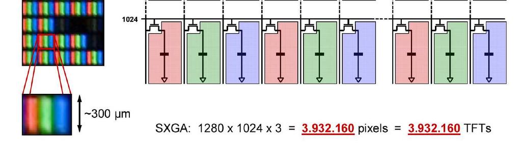
33 OLE Based isplays Emissive front end FETs can be larger in top emitting device, but multiple FETs/pixel (smaller Mobility cm 2 /Vs 1 Colour, high performance displays ONY W/pixel than EP ) Current driven device - demands transistor performance uniformity and stability E-Paper (small rollable displays) Large area (low performance) Achievable by solution processed materials Time to launch Polymer Vision Compatible with OFET performance Reflective effect OFETs can be larger (i.e. lower µ requirements) Low refresh rates lower pixel charging speeds lower µ requirements Bistable - lower duty cycle, longer lifetimes. Higher resolution and size require larger number of rows/columns higher I ON and faster charging speeds - higher µ. OFET Applications in Optical isplays AM-LC V ata Mobility cm 2 /Vs 1 Colour, high Performance displays V Address 1-1 Large area (low performance) witch GN LC pixel E-Paper (small rollable displays) Achievable by polymers 28 Time to launch AM-OLE V ata Mobility cm 2 /Vs 1 High efficiency OLE devices Colour, high Performance displays V Address V 1-1 Large area (low performance) T1 T2 - driver 1-2 E-Paper (small rollable displays) C OLE GN Achievable by polymers Time to launch 33


34 Active-Matrix Liquid Crystal isplays (LCs) Active-Matrix Liquid Crystal isplays (LCs) 34
 witch GN LC pixel 1-2 1-3")

 C OLE GN 1-3 28 Achievable by polymers Time to launch Active-Matrix OLE based")
35 OFET Applications in Optical isplays AM-LC V ata Mobility cm 2 /Vs 1 Colour, high Performance displays V Address 1-1 Large area (low performance) witch GN LC pixel E-Paper (small rollable displays) Achievable by polymers 28 Time to launch AM-OLE V ata Mobility cm 2 /Vs 1 High efficiency OLE devices Colour, high Performance displays V Address V 1-1 Large area (low performance) T1 T2 - driver 1-2 E-Paper (small rollable displays) C OLE GN Achievable by polymers Time to launch Active-Matrix OLE based isplays (AM-OLEs) 35
36 OTFTs in microelectronics OTFTs emiconductor emiconductor ielectric Gate Bottom-Gate, Bottom-Contact ielectric Gate Bottom-Gate, Top-Contact Gate ielectric Gate ielectric emiconductor emiconductor ubstrate ubstrate 36
37 The Voltage Inverter IN OUT IN 1 OUT 1 Voltage inverter The Voltage Inverter IN OUT Gain = V OUT / V IN IN 1 OUT 1 V OUT (V) Voltage inverter -2-2 V IN (V) 37
38 The Voltage Inverter IN OUT Gain = V OUT / V IN IN 1 OUT 1 V OUT (V) Voltage inverter -2-2 V IN (V) The Voltage Inverter IN OUT Noise Margin Gain = V OUT / V IN IN 1 OUT 1 V OUT (V) NM max NM = V IN /2 Noise Margin Voltage inverter -2-2 V IN (V) 38
39 The Voltage Inverter IN OUT IN 1 OUT V OUT (V) Unipolar inverter circuit based on pentacene 1 Voltage inverter V IN (V) The Voltage Inverter High NM Noise Margin Gain = V OUT / V IN V OUT (V) IN OUT Noise Margin -2-2 V IN (V) 39
40 The Voltage Inverter High NM Noise Margin Gain = V OUT / V IN HIGH V OUT (V) IN OUT Noise Margin LOW -2-2 V IN (V) The Voltage Inverter High NM Noise Margin Gain = V OUT / V IN HIGH V OUT (V) IN OUT Noise Margin LOW -2-2 V IN (V) Circuits with high NM can tolerate input noise. 4
41 The Voltage Inverter Low NM HIGH V OUT (V) IN OUT LOW V IN (V) The Voltage Inverter Low NM HIGH V OUT (V) IN OUT LOW V IN (V) 41
42 The Voltage Inverter Low NM HIGH V OUT (V) IN OUT LOW V IN (V) Circuits with small NM are highly sensitive to input/signal noise ifferent Logic Families - V V V OFET 1 p-type Ambipolar V OUT V IN V OUT V IN V OUT -V IN OFET 2 n-type Ambipolar Unipolar (V G = V) Complementary Complementary-likelike 42
43 Unipolar Logic V G = V, Logic iode-load Logic V V IN T OUT IN T OUT T L T L GN GN Choice of logic depends on the operating characteristics of the individual OFETs Unipolar Logic V OFET 1 V OUT V IN OFET 2 Unipolar (V G = V) 43
44 Unipolar Logic V V OFET 1 R1 V OUT V IN = LOW V IN OFET 2 R2 = GN V OUT = V Unipolar (V G = V) V OUT = High Unipolar Logic V V V OFET 1 R1 R1 = V OUT V IN = LOW V IN = HIGH V IN OFET 2 R2 = GN V OUT = V GN R2 V OUT = GN Unipolar (V G = V) V OUT = High V OUT = Low 44
 High power consumption 45")
45 Unipolar Logic V OFET 1 OFET 1 V OUT V IN OFET 2 OFET 2 Unipolar (V G = V) Unipolar organic inverter Unipolar Logic V V IN OFET 1 V OUT OFET 2 Unipolar (V G = V) imple fabrication - ingle semiconductor - ingle contact material Complex design -Extra vertical interconnects Poor noise margins -Low yield (i.e. high cost) High power consumption 45
46 Unipolar Logic V -1. V IN OFET 1 V OUT OFET 2 V OUT (V) T1: L=1, W=1 T2: L=1, W= tatic power (a.u.) Unipolar (V G = V) V IN (V). Complementary Logic IN V T PU T P OUT Complementary logic circuits: Complementary logic is the dominant logic used in ibased electronics. This is due to its high performance characteristics i.e.: GN High gain Low static-power dissipation Excellent noise margin 46
47 Complementary Logic V p-type V IN V OUT n-type Complementary Complementary Logic V V p-type R1 V IN V OUT V IN = LOW n-type R2 = GN V OUT = V Complementary V OUT = High 47
48 Complementary Logic V V V p-type R1 R1 = V IN V OUT V IN = LOW V IN = HIGH n-type R2 = GN V OUT = V GN R2 V OUT = GN Complementary V OUT = High V OUT = Low Complementary Logic V IN V p-type n-type V OUT imple design - Minimum interconnects Low power consumption High noise margins - i.e. high yield Complex fabrication - Two semiconductors - Two electrode materials Complementary Complementary organic circuits 48
49 Complementary Logic V V IN p-type n-type V OUT V OUT (V) T1: L=1, W=2 T2: L=1, W= tatic power (a.u.) Complementary V IN (V). Unipolar vs. Complementary Logic V V OFET 1 p-type V OUT V IN V OUT V IN OFET 2 n-type Unipolar (V G = V) Complementary 5 V OUT (V) V OUT (V) V IN (V) Unipolar V IN (V) Complementary 49
50 Ring Oscillator cope 1st n GN A ring oscillator is a concatenation of an odd number of inverters, as shown in the figure above. uch circuits can provide valuable information related to: evice/material processing Circuit layout Material properties (mobility, parameter uniformity, stability etc.) Ring Oscillator cope 1st n GN L 5
51 Ring Oscillator cope 1st n GN L H Ring Oscillator Output(n) Input(1 st ) cope 1st n GN L H L H When output(n) input(1st) the circuit oscillates 51
 f OC = (2 n τ INV ) -1 Unipolar polymer-based ring-oscillators Ring Oscillator state-of of-the-art V Blend OFET Output Input Blend OFET Ground Input")
 dif-at:ptaa -2-4 -6-8 -1-12 V (Volt) High performance 7-stages ring-oscillators (L = 1.")
52 Ring Oscillator state-of of-the-art Output(n) J. Mater. Res., 19, 1963 (24) f OC = (2 n τ INV ) -1 Unipolar polymer-based ring-oscillators Ring Oscillator state-of of-the-art V Blend OFET Output Input Blend OFET Ground Input Output 7-stage ring oscillator (p-type) f OC (khz) Output signal (a.u.) Time (µs) F TE TE V = -12 V f OC (khz) * * n F N R V = -6 V -75 V -1 V -12 V Channel length (µm ) dif-at:ptaa V (Volt) High performance 7-stages ring-oscillators (L = 1.5 µm) based on BG-BC OFETs Oscillation frequency ~ 1 khz tage delay ~ 712 ns J. mith et al. Appl. Phys. Lett. 93, (28) 52
 mall-molecule molecule complementary ring-oscillators Ring Oscillator state-of of-the-art Complexity Unipolar logic: 1888 transistors @ 5 khz [1] High power dissipation imple")
53 Ring Oscillator state-of of-the-art J. Appl. Phys., 89, 5125 (21) mall-molecule molecule complementary ring-oscillators Ring Oscillator state-of of-the-art Complexity Unipolar logic: khz [1] High power dissipation imple technology Low yield Complementary logic: khz [2] Low power dissipation Complicated technology High yield [1] Nature Materials 3, 16 (24) [2] Nature 43, 521 (2) peed Unipolar circuits: Poly-3alkylthiophene based ringoscillators [3] : 22 ms Complementary circuits: H-a5T and F 16 CuPc based ringoscillators [4] : 1 1 ms [3] J. Mater. Res., 19, 1963 (24) [4] J. Appl. Phys., 89, 5125 (21) 53
54 Thank you 54
Lecture 2 Thin Film Transistors
 Lecture 2 Thin Film Transistors 1/60 Announcements Homework 1/4: Will be online after the Lecture on Tuesday October 2 nd. Total of 25 marks. Each homework contributes an equal weight. All homework contributes
Field-Effect (FET) transistors
 transistors") Field-Effect (FET) transistors References: Barbow (Chapter 8), Rizzoni (chapters 8 & 9) In a field-effect transistor (FET), the width of a conducting channel in a semiconductor and, therefore, its current-carrying
Field-Effect (FET) transistors References: Barbow (Chapter 8), Rizzoni (chapters 8 & 9) In a field-effect transistor (FET), the width of a conducting channel in a semiconductor and, therefore, its current-carrying
FIELD EFFECT TRANSISTORS:
 Chapter 10 FIEL EFFECT TRANITOR: MOFET The following overview gures describe important issues related to the most important electronic device. NUMBER OF ACTIVE EVICE/CHIP MOORE' LAW Gordon Moore, co-founder
Enhancing the Performance of Organic Thin-Film Transistor using a Buffer Layer
 Proceedings of the 9th International Conference on Properties and Applications of Dielectric Materials July 19-23, 29, Harbin, China L-7 Enhancing the Performance of Organic Thin-Film Transistor using
Semiconductor Polymer
 Semiconductor Polymer Organic Semiconductor for Flexible Electronics Introduction: An organic semiconductor is an organic compound that possesses similar properties to inorganic semiconductors with hole
Lecture 17 Field-Effect Transistors 2
 Lecture 17 Field-Effect Transistors chroder: Chapters, 4, 6 1/57 Announcements Homework 4/6: Is online now. ue Monday May 1st at 10:00am. I will return it the following Monday (8 th May). Homework 5/6:
Chapter 4 Field-Effect Transistors
 Chapter 4 Field-Effect Transistors Microelectronic Circuit Design Richard C. Jaeger Travis N. Blalock 5/5/11 Chap 4-1 Chapter Goals Describe operation of MOSFETs. Define FET characteristics in operation
ECE 546 Lecture 10 MOS Transistors
 ECE 546 Lecture 10 MOS Transistors Spring 2018 Jose E. Schutt-Aine Electrical & Computer Engineering University of Illinois jesa@illinois.edu NMOS Transistor NMOS Transistor N-Channel MOSFET Built on p-type
MOS Transistor Theory
 MOS Transistor Theory So far, we have viewed a MOS transistor as an ideal switch (digital operation) Reality: less than ideal EE 261 Krish Chakrabarty 1 Introduction So far, we have treated transistors
Lecture 12: MOS Capacitors, transistors. Context
 Lecture 12: MOS Capacitors, transistors Context In the last lecture, we discussed PN diodes, and the depletion layer into semiconductor surfaces. Small signal models In this lecture, we will apply those
Class 05: Device Physics II
 Topics: 1. Introduction 2. NFET Model and Cross Section with Parasitics 3. NFET as a Capacitor 4. Capacitance vs. Voltage Curves 5. NFET as a Capacitor - Band Diagrams at V=0 6. NFET as a Capacitor - Accumulation
Transistors - a primer
 ransistors - a primer What is a transistor? Solid-state triode - three-terminal device, with voltage (or current) at third terminal used to control current between other two terminals. wo types: bipolar
Low Power VLSI Circuits and Systems Prof. Ajit Pal Department of Computer Science and Engineering Indian Institute of Technology, Kharagpur
 Low Power VLSI Circuits and Systems Prof. Ajit Pal Department of Computer Science and Engineering Indian Institute of Technology, Kharagpur Lecture No. # 08 MOS Inverters - III Hello, and welcome to today
MOS Transistors. Prof. Krishna Saraswat. Department of Electrical Engineering Stanford University Stanford, CA
 MOS Transistors Prof. Krishna Saraswat Department of Electrical Engineering S Stanford, CA 94305 saraswat@stanford.edu 1 1930: Patent on the Field-Effect Transistor! Julius Lilienfeld filed a patent describing
Digital Electronics Part II - Circuits
 Digital Electronics Part - Circuits Dr.. J. Wassell Gates from Transistors ntroduction Logic circuits are non-linear, consequently we will introduce a graphical technique for analysing such circuits The
The Intrinsic Silicon
 The Intrinsic ilicon Thermally generated electrons and holes Carrier concentration p i =n i ni=1.45x10 10 cm-3 @ room temp Generally: n i = 3.1X10 16 T 3/2 e -1.21/2KT cm -3 T= temperature in K o (egrees
Fig. 1 CMOS Transistor Circuits (a) Inverter Out = NOT In, (b) NOR-gate C = NOT (A or B)
 Inverter Out = NOT In, (b) NOR-gate C = NOT (A or B)") 1 Introduction to Transistor-Level Logic Circuits 1 By Prawat Nagvajara At the transistor level of logic circuits, transistors operate as switches with the logic variables controlling the open or closed
1 Introduction to Transistor-Level Logic Circuits 1 By Prawat Nagvajara At the transistor level of logic circuits, transistors operate as switches with the logic variables controlling the open or closed
Lecture #39. Transistor Scaling
 Lecture #39 ANNOUNCEMENT Pick up graded HW assignments and exams (78 Cory) Lecture #40 will be the last formal lecture. Class on Friday will be dedicated to a course review (with sample problems). Discussion
Announcements. EE105 - Fall 2005 Microelectronic Devices and Circuits. Lecture Material. MOS CV Curve. MOSFET Cross Section
 Announcements EE0 - Fall 00 Microelectronic evices and Circuits ecture 7 Homework, due today Homework due net week ab this week Reading: Chapter MO Transistor ecture Material ast lecture iode currents
MOSFET: Introduction
 E&CE 437 Integrated VLSI Systems MOS Transistor 1 of 30 MOSFET: Introduction Metal oxide semiconductor field effect transistor (MOSFET) or MOS is widely used for implementing digital designs Its major
Thin Film Transistors (TFT)
") Thin Film Transistors (TFT) a-si TFT - α-si:h (Hydrogenated amorphous Si) deposited with a PECVD system (low temp. process) replaces the single crystal Si substrate. - Inverted staggered structure with
Thin Film Transistors (TFT) a-si TFT - α-si:h (Hydrogenated amorphous Si) deposited with a PECVD system (low temp. process) replaces the single crystal Si substrate. - Inverted staggered structure with
Section 12: Intro to Devices
 Section 12: Intro to Devices Extensive reading materials on reserve, including Robert F. Pierret, Semiconductor Device Fundamentals Bond Model of Electrons and Holes Si Si Si Si Si Si Si Si Si Silicon
6.012 Electronic Devices and Circuits
 Page 1 of 10 YOUR NAME Department of Electrical Engineering and Computer Science Massachusetts Institute of Technology 6.012 Electronic Devices and Circuits Exam No. 2 Thursday, November 5, 2009 7:30 to
Fundamentals of the Metal Oxide Semiconductor Field-Effect Transistor
 Triode Working FET Fundamentals of the Metal Oxide Semiconductor Field-Effect Transistor The characteristics of energy bands as a function of applied voltage. Surface inversion. The expression for the
MOS Transistor Theory
 CHAPTER 3 MOS Transistor Theory Outline 2 1. Introduction 2. Ideal I-V Characteristics 3. Nonideal I-V Effects 4. C-V Characteristics 5. DC Transfer Characteristics 6. Switch-level RC Delay Models MOS
Section 12: Intro to Devices
 Section 12: Intro to Devices Extensive reading materials on reserve, including Robert F. Pierret, Semiconductor Device Fundamentals EE143 Ali Javey Bond Model of Electrons and Holes Si Si Si Si Si Si Si
ESE 570: Digital Integrated Circuits and VLSI Fundamentals
 ESE 570: Digital Integrated Circuits and VLSI Fundamentals Lec 4: January 23, 2018 MOS Transistor Theory, MOS Model Penn ESE 570 Spring 2018 Khanna Lecture Outline! CMOS Process Enhancements! Semiconductor
Plastic Electronics. Joaquim Puigdollers.
 Plastic Electronics Joaquim Puigdollers Joaquim.puigdollers@upc.edu Nobel Prize Chemistry 2000 Origins Technological Interest First products.. MONOCROMATIC PHILIPS Today Future Technological interest Low
Long Channel MOS Transistors
 Long Channel MOS Transistors The theory developed for MOS capacitor (HO #2) can be directly extended to Metal-Oxide-Semiconductor Field-Effect transistors (MOSFET) by considering the following structure:
Supporting Information
 Supporting Information Monolithically Integrated Flexible Black Phosphorus Complementary Inverter Circuits Yuanda Liu, and Kah-Wee Ang* Department of Electrical and Computer Engineering National University
MOS Transistor I-V Characteristics and Parasitics
 ECEN454 Digital Integrated Circuit Design MOS Transistor I-V Characteristics and Parasitics ECEN 454 Facts about Transistors So far, we have treated transistors as ideal switches An ON transistor passes
ECE 342 Electronic Circuits. 3. MOS Transistors
 ECE 342 Electronic Circuits 3. MOS Transistors Jose E. Schutt-Aine Electrical & Computer Engineering University of Illinois jschutt@emlab.uiuc.edu 1 NMOS Transistor Typically L = 0.1 to 3 m, W = 0.2 to
Lecture 3: CMOS Transistor Theory
 Lecture 3: CMOS Transistor Theory Outline Introduction MOS Capacitor nmos I-V Characteristics pmos I-V Characteristics Gate and Diffusion Capacitance 2 Introduction So far, we have treated transistors
Course Administration. CPE/EE 427, CPE 527 VLSI Design I L04: MOS Transistors. Review: CMOS Process at a Glance
 Course Administration CPE/EE 7, CPE 7 VLI esign I L: MO Transistors epartment of Electrical and Computer Engineering University of Alabama in Huntsville Aleksandar Milenkovic ( www.ece.uah.edu/~milenka
Lecture 12: MOSFET Devices
 Lecture 12: MOSFET Devices Gu-Yeon Wei Division of Engineering and Applied Sciences Harvard University guyeon@eecs.harvard.edu Wei 1 Overview Reading S&S: Chapter 5.1~5.4 Supplemental Reading Background
ECE 340 Lecture 39 : MOS Capacitor II
 ECE 340 Lecture 39 : MOS Capacitor II Class Outline: Effects of Real Surfaces Threshold Voltage MOS Capacitance-Voltage Analysis Things you should know when you leave Key Questions What are the effects
EE105 - Fall 2005 Microelectronic Devices and Circuits
 EE105 - Fall 005 Microelectronic Devices and Circuits ecture 7 MOS Transistor Announcements Homework 3, due today Homework 4 due next week ab this week Reading: Chapter 4 1 ecture Material ast lecture
ESE 570: Digital Integrated Circuits and VLSI Fundamentals
 ESE 570: Digital Integrated Circuits and VLSI Fundamentals Lec 4: January 29, 2019 MOS Transistor Theory, MOS Model Penn ESE 570 Spring 2019 Khanna Lecture Outline! CMOS Process Enhancements! Semiconductor
Chapter 2. Design and Fabrication of VLSI Devices
 Chapter 2 Design and Fabrication of VLSI Devices Jason Cong 1 Design and Fabrication of VLSI Devices Objectives: To study the materials used in fabrication of VLSI devices. To study the structure of devices
EE105 - Fall 2006 Microelectronic Devices and Circuits
 EE105 - Fall 2006 Microelectronic Devices and Circuits Prof. Jan M. Rabaey (jan@eecs) Lecture 7: MOS Transistor Some Administrative Issues Lab 2 this week Hw 2 due on We Hw 3 will be posted same day MIDTERM
MOS Transistor Properties Review
 MOS Transistor Properties Review 1 VLSI Chip Manufacturing Process Photolithography: transfer of mask patterns to the chip Diffusion or ion implantation: selective doping of Si substrate Oxidation: SiO
Lecture 04 Review of MOSFET
 ECE 541/ME 541 Microelectronic Fabrication Techniques Lecture 04 Review of MOSFET Zheng Yang (ERF 3017, email: yangzhen@uic.edu) What is a Transistor? A Switch! An MOS Transistor V GS V T V GS S Ron D
Organic Electronic Devices
 Organic Electronic Devices Week 5: Organic Light-Emitting Devices and Emerging Technologies Lecture 5.5: Course Review and Summary Bryan W. Boudouris Chemical Engineering Purdue University 1 Understanding
MOS CAPACITOR AND MOSFET
 EE336 Semiconductor Devices 1 MOS CAPACITOR AND MOSFET Dr. Mohammed M. Farag Ideal MOS Capacitor Semiconductor Devices Physics and Technology Chapter 5 EE336 Semiconductor Devices 2 MOS Capacitor Structure
Review of Band Energy Diagrams MIS & MOS Capacitor MOS TRANSISTORS MOSFET Capacitances MOSFET Static Model
 Content- MOS Devices and Switching Circuits Review of Band Energy Diagrams MIS & MOS Capacitor MOS TRANSISTORS MOSFET Capacitances MOSFET Static Model A Cantoni 2009-2013 Digital Switching 1 Content- MOS
CMPEN 411 VLSI Digital Circuits. Lecture 03: MOS Transistor
 CMPEN 411 VLSI Digital Circuits Lecture 03: MOS Transistor Kyusun Choi [Adapted from Rabaey s Digital Integrated Circuits, Second Edition, 2003 J. Rabaey, A. Chandrakasan, B. Nikolic] CMPEN 411 L03 S.1
ECE 342 Electronic Circuits. Lecture 6 MOS Transistors
 ECE 342 Electronic Circuits Lecture 6 MOS Transistors Jose E. Schutt-Aine Electrical & Computer Engineering University of Illinois jesa@illinois.edu 1 NMOS Transistor Typically L = 0.1 to 3 m, W = 0.2
6.012 Electronic Devices and Circuits
 Page 1 of 12 YOUR NAME Department of Electrical Engineering and Computer Science Massachusetts Institute of Technology 6.012 Electronic Devices and Circuits FINAL EXAMINATION Open book. Notes: 1. Unless
Field effect = Induction of an electronic charge due to an electric field Example: Planar capacitor
 JFETs AND MESFETs Introduction Field effect = Induction of an electronic charge due to an electric field Example: Planar capacitor Why would an FET made of a planar capacitor with two metal plates, as
Electronics Fets and Mosfets Prof D C Dube Department of Physics Indian Institute of Technology, Delhi
 Electronics Fets and Mosfets Prof D C Dube Department of Physics Indian Institute of Technology, Delhi Module No. #05 Lecture No. #02 FETS and MOSFETS (contd.) In the previous lecture, we studied the working
Choice of V t and Gate Doping Type
 Choice of V t and Gate Doping Type To make circuit design easier, it is routine to set V t at a small positive value, e.g., 0.4 V, so that, at V g = 0, the transistor does not have an inversion layer and
Semiconductor Physics Problems 2015
 Semiconductor Physics Problems 2015 Page and figure numbers refer to Semiconductor Devices Physics and Technology, 3rd edition, by SM Sze and M-K Lee 1. The purest semiconductor crystals it is possible
VLSI Design I; A. Milenkovic 1
 Review: implified CMO Inverter Process CPE/EE 7, CPE 7 VLI esign I L: MO Transistor cut line epartment of Electrical and Computer Engineering University of Alabama in Huntsville Aleksandar Milenkovic (
Important! EE141- Fall 2002 Lecture 5. CMOS Inverter MOS Transistor Model
 - Fall 00 Lecture 5 CMO Inverter MO Transistor Model Important! Lab 3 this week You must show up in one of the lab sessions this week If you don t show up you will be dropped from the class» Unless you
ECE 497 JS Lecture - 12 Device Technologies
 ECE 497 JS Lecture - 12 Device Technologies Spring 2004 Jose E. Schutt-Aine Electrical & Computer Engineering University of Illinois jose@emlab.uiuc.edu 1 NMOS Transistor 2 ρ Source channel charge density
Metal-oxide-semiconductor field effect transistors (2 lectures)
") Metal-ide-semiconductor field effect transistors ( lectures) MOS physics (brief in book) Current-voltage characteristics - pinch-off / channel length modulation - weak inversion - velocity saturation -
Metal-ide-semiconductor field effect transistors ( lectures) MOS physics (brief in book) Current-voltage characteristics - pinch-off / channel length modulation - weak inversion - velocity saturation -
FIELD-EFFECT TRANSISTORS
 FIEL-EFFECT TRANSISTORS 1 Semiconductor review 2 The MOS capacitor 2 The enhancement-type N-MOS transistor 3 I-V characteristics of enhancement MOSFETS 4 The output characteristic of the MOSFET in saturation
Extensive reading materials on reserve, including
 Section 12: Intro to Devices Extensive reading materials on reserve, including Robert F. Pierret, Semiconductor Device Fundamentals EE143 Ali Javey Bond Model of Electrons and Holes Si Si Si Si Si Si Si
Lecture 15: MOS Transistor models: Body effects, SPICE models. Context. In the last lecture, we discussed the modes of operation of a MOS FET:
 Lecture 15: MOS Transistor models: Body effects, SPICE models Context In the last lecture, we discussed the modes of operation of a MOS FET: oltage controlled resistor model I- curve (Square-Law Model)
Lecture 15 OUTLINE. MOSFET structure & operation (qualitative) Review of electrostatics The (N)MOS capacitor
 Review of electrostatics The (N)MOS capacitor") Lecture 15 OUTLINE MOSFET structure & operation (qualitative) Review of electrostatics The (N)MOS capacitor Electrostatics Charge vs. voltage characteristic Reading: Chapter 6.1 6.2.1 EE15 Spring 28 Lecture
Lecture 15 OUTLINE MOSFET structure & operation (qualitative) Review of electrostatics The (N)MOS capacitor Electrostatics Charge vs. voltage characteristic Reading: Chapter 6.1 6.2.1 EE15 Spring 28 Lecture
EEC 116 Lecture #3: CMOS Inverters MOS Scaling. Rajeevan Amirtharajah University of California, Davis Jeff Parkhurst Intel Corporation
 EEC 116 Lecture #3: CMOS Inverters MOS Scaling Rajeevan Amirtharajah University of California, Davis Jeff Parhurst Intel Corporation Outline Review: Inverter Transfer Characteristics Lecture 3: Noise Margins,
EE 330 Lecture 6. Improved Switch-Level Model Propagation Delay Stick Diagrams Technology Files
 EE 330 Lecture 6 Improved witch-level Model Propagation elay tick iagrams Technology Files Review from Last Time MO Transistor Qualitative iscussion of n-channel Operation Bulk ource Gate rain rain G Gate
Classification of Solids
 Classification of Solids Classification by conductivity, which is related to the band structure: (Filled bands are shown dark; D(E) = Density of states) Class Electron Density Density of States D(E) Examples
VLSI GATE LEVEL DESIGN UNIT - III P.VIDYA SAGAR ( ASSOCIATE PROFESSOR) Department of Electronics and Communication Engineering, VBIT
 Department of Electronics and Communication Engineering, VBIT") VLSI UNIT - III GATE LEVEL DESIGN P.VIDYA SAGAR ( ASSOCIATE PROFESSOR) contents GATE LEVEL DESIGN : Logic Gates and Other complex gates, Switch logic, Alternate gate circuits, Time Delays, Driving large
VLSI UNIT - III GATE LEVEL DESIGN P.VIDYA SAGAR ( ASSOCIATE PROFESSOR) contents GATE LEVEL DESIGN : Logic Gates and Other complex gates, Switch logic, Alternate gate circuits, Time Delays, Driving large
Stretching the Barriers An analysis of MOSFET Scaling. Presenters (in order) Zeinab Mousavi Stephanie Teich-McGoldrick Aseem Jain Jaspreet Wadhwa
 Zeinab Mousavi Stephanie Teich-McGoldrick Aseem Jain Jaspreet Wadhwa") Stretching the Barriers An analysis of MOSFET Scaling Presenters (in order) Zeinab Mousavi Stephanie Teich-McGoldrick Aseem Jain Jaspreet Wadhwa Why Small? Higher Current Lower Gate Capacitance Higher
Stretching the Barriers An analysis of MOSFET Scaling Presenters (in order) Zeinab Mousavi Stephanie Teich-McGoldrick Aseem Jain Jaspreet Wadhwa Why Small? Higher Current Lower Gate Capacitance Higher
Lecture 6 PN Junction and MOS Electrostatics(III) Metal-Oxide-Semiconductor Structure
 Metal-Oxide-Semiconductor Structure") Lecture 6 PN Junction and MOS Electrostatics(III) Metal-Oxide-Semiconductor Structure Outline 1. Introduction to MOS structure 2. Electrostatics of MOS in thermal equilibrium 3. Electrostatics of MOS with
Lecture 6 PN Junction and MOS Electrostatics(III) Metal-Oxide-Semiconductor Structure Outline 1. Introduction to MOS structure 2. Electrostatics of MOS in thermal equilibrium 3. Electrostatics of MOS with
ECE606: Solid State Devices Lecture 22 MOScap Frequency Response MOSFET I-V Characteristics
 EE66: olid tate evices Lecture 22 MOcap Frequency Response MOFET I- haracteristics erhard Klimeck gekco@purdue.edu. Background 2. mall signal capacitances 3. Large signal capacitance 4. Intermediate ummary
Integrated Circuits & Systems
 Federal University of Santa Catarina Center for Technology Computer Science & Electronics Engineering Integrated Circuits & Systems INE 5442 Lecture 10 MOSFET part 1 guntzel@inf.ufsc.br ual-well Trench-Isolated
B.Supmonchai June 26, q Introduction of device basic equations. q Introduction of models for manual analysis.
 June 26, 2004 oal of this chapter Chapter 2 MO Transistor Theory oonchuay upmonchai Integrated esign Application Research (IAR) Laboratory June 16th, 2004; Revised June 16th, 2005 q Present intuitive understanding
Halbleiter Prof. Yong Lei Prof. Thomas Hannappel
 Halbleiter Prof. Yong Lei Prof. Thomas Hannappel yong.lei@tu-ilmenau.de thomas.hannappel@tu-ilmenau.de http://www.tu-ilmenau.de/nanostruk/ Organic Semiconductors & Organic Electronics Organic semiconductors
6.012 Electronic Devices and Circuits Spring 2005
 6.012 Electronic Devices and Circuits Spring 2005 May 16, 2005 Final Exam (200 points) -OPEN BOOK- Problem NAME RECITATION TIME 1 2 3 4 5 Total General guidelines (please read carefully before starting):
organic semiconductors Henning Sirringhaus
 Charge transport physics of highmobility organic semiconductors Henning irringhaus Organic electronics tatus and opportunities OLED Existing markets Emerging applications Advanced prototypes Next generation
an introduction to Semiconductor Devices
 an introduction to Semiconductor Devices Donald A. Neamen Chapter 6 Fundamentals of the Metal-Oxide-Semiconductor Field-Effect Transistor Introduction: Chapter 6 1. MOSFET Structure 2. MOS Capacitor -
ESE 570: Digital Integrated Circuits and VLSI Fundamentals
 EE 570: igital Integrated Circuits and VLI Fundamentals Lec 2: January 22, 2019 MO Fabrication pt. 1: Physics and Methodology Lecture Outline! igital CMO Basics! VLI Fundamentals! Fabrication Process 2
VLSI Design I; A. Milenkovic 1
 ourse dministration PE/EE 47, PE 57 VLI esign I L6: tatic MO Logic epartment of Electrical and omputer Engineering University of labama in Huntsville leksandar Milenkovic ( www. ece.uah.edu/~milenka )
! CMOS Process Enhancements. ! Semiconductor Physics. " Band gaps. " Field Effects. ! MOS Physics. " Cut-off. " Depletion.
 ESE 570: Digital Integrated Circuits and VLSI Fundamentals Lec 4: January 3, 018 MOS Transistor Theory, MOS Model Lecture Outline! CMOS Process Enhancements! Semiconductor Physics " Band gaps " Field Effects!
Electronic Circuits 1. Transistor Devices. Contents BJT and FET Characteristics Operations. Prof. C.K. Tse: Transistor devices
 Electronic Circuits 1 Transistor Devices Contents BJT and FET Characteristics Operations 1 What is a transistor? Three-terminal device whose voltage-current relationship is controlled by a third voltage
VLSI Design I; A. Milenkovic 1
 PE/EE 47, PE 57 VLI esign I L6: tatic MO Logic epartment of Electrical and omputer Engineering University of labama in Huntsville leksandar Milenkovic ( www. ece.uah.edu/~milenka ) www. ece.uah.edu/~milenka/cpe57-3f
MOS Capacitors ECE 2204
 MOS apacitors EE 2204 Some lasses of Field Effect Transistors Metal-Oxide-Semiconductor Field Effect Transistor MOSFET, which will be the type that we will study in this course. Metal-Semiconductor Field
SECTION: Circle one: Alam Lundstrom. ECE 305 Exam 5 SOLUTIONS: Spring 2016 April 18, 2016 M. A. Alam and M.S. Lundstrom Purdue University
 NAME: PUID: SECTION: Circle one: Alam Lundstrom ECE 305 Exam 5 SOLUTIONS: April 18, 2016 M A Alam and MS Lundstrom Purdue University This is a closed book exam You may use a calculator and the formula
! CMOS Process Enhancements. ! Semiconductor Physics. " Band gaps. " Field Effects. ! MOS Physics. " Cut-off. " Depletion.
 ESE 570: Digital Integrated Circuits and VLSI Fundamentals Lec 4: January 9, 019 MOS Transistor Theory, MOS Model Lecture Outline CMOS Process Enhancements Semiconductor Physics Band gaps Field Effects
Lecture 4: CMOS Transistor Theory
 Introduction to CMOS VLSI Design Lecture 4: CMOS Transistor Theory David Harris, Harvey Mudd College Kartik Mohanram and Steven Levitan University of Pittsburgh Outline q Introduction q MOS Capacitor q
High Performance, Low Operating Voltage n-type Organic Field Effect Transistor Based on Inorganic-Organic Bilayer Dielectric System
 Journal of Physics: Conference Series PAPER OPEN ACCESS High Performance, Low Operating Voltage n-type Organic Field Effect Transistor Based on Inorganic-Organic Bilayer Dielectric System To cite this
SEMINAR. Organic Semiconductor Thin Film Transistors
 University of Ljubljana Faculty of Mathematics and Physics Department of Physics SEMINAR Organic Semiconductor Thin Film Transistors Author: Tomaž Mlakar Adviser: Dr. Gvido Bratina Nova Gorica Polytechnic
Lecture 15 OUTLINE. MOSFET structure & operation (qualitative) Review of electrostatics The (N)MOS capacitor
 Review of electrostatics The (N)MOS capacitor") Lecture 15 OUTLINE MOSFET structure & operation (qualitative) Review of electrostatics The (N)MOS capacitor Electrostatics t ti Charge vs. voltage characteristic Reading: Chapter 6.1 6.2.1 EE105 Fall 2007
Lecture 15 OUTLINE MOSFET structure & operation (qualitative) Review of electrostatics The (N)MOS capacitor Electrostatics t ti Charge vs. voltage characteristic Reading: Chapter 6.1 6.2.1 EE105 Fall 2007
EE 4345 Chapter 6. Derek Johnson Michael Hasni Rex Reeves Michael Custer
 EE 4345 Chapter 6 Derek Johnson Michael Hasni Rex Reeves Michael Custer Coupling AC Signals Constructing timing networks Constructing phase shift networks Feedback loop compensation Semiconductors use:
KINGS COLLEGE OF ENGINEERING DEPARTMENT OF ELECTRONICS AND COMMUNICATION ENGINEERING QUESTION BANK
 KINGS COLLEGE OF ENGINEERING DEPARTMENT OF ELECTRONICS AND COMMUNICATION ENGINEERING QUESTION BANK SUBJECT CODE: EC 1354 SUB.NAME : VLSI DESIGN YEAR / SEMESTER: III / VI UNIT I MOS TRANSISTOR THEORY AND
Charge Storage in the MOS Structure. The Inverted MOS Capacitor (V GB > V Tn )
") The Inverted MO Capacitor (V > V Tn ) We consider the surface potential as Þxed (ÒpinnedÓ) at φ s,max = - φ p φ(x).5 V. V V ox Charge torage in the MO tructure Three regions of operation: Accumulation:
The Inverted MO Capacitor (V > V Tn ) We consider the surface potential as Þxed (ÒpinnedÓ) at φ s,max = - φ p φ(x).5 V. V V ox Charge torage in the MO tructure Three regions of operation: Accumulation:
Review of Semiconductor Physics. Lecture 3 4 Dr. Tayab Din Memon
 Review of Semiconductor Physics Lecture 3 4 Dr. Tayab Din Memon 1 Electronic Materials The goal of electronic materials is to generate and control the flow of an electrical current. Electronic materials
Lecture 23. Dealing with Interconnect. Impact of Interconnect Parasitics
 Lecture 23 Dealing with Interconnect Impact of Interconnect Parasitics Reduce Reliability Affect Performance Classes of Parasitics Capacitive Resistive Inductive 1 INTERCONNECT Dealing with Capacitance
EE 330 Lecture 6. Improved Switch-Level Model Propagation Delay Stick Diagrams Technology Files - Design Rules
 EE 330 Lecture 6 Improved witch-level Model Propagation elay tick iagrams Technology Files - esign Rules Review from Last Time MO Transistor Qualitative iscussion of n-channel Operation Bulk ource Gate
Lecture 11: MOS Transistor
 Lecture 11: MOS Transistor Prof. Niknejad Lecture Outline Review: MOS Capacitors Regions MOS Capacitors (3.8 3.9) CV Curve Threshold Voltage MOS Transistors (4.1 4.3): Overview Cross-section and layout
Introduction to CMOS VLSI. Chapter 2: CMOS Transistor Theory. Harris, 2004 Updated by Li Chen, Outline
 Introduction to MOS VLSI Design hapter : MOS Transistor Theory copyright@david Harris, 004 Updated by Li hen, 010 Outline Introduction MOS apacitor nmos IV haracteristics pmos IV haracteristics Gate and
Lecture 2. Introduction to semiconductors Structures and characteristics in semiconductors
 Lecture 2 Introduction to semiconductors Structures and characteristics in semiconductors Semiconductor p-n junction Metal Oxide Silicon structure Semiconductor contact Literature Glen F. Knoll, Radiation
GaN based transistors
 GaN based transistors S FP FP dielectric G SiO 2 Al x Ga 1-x N barrier i-gan Buffer i-sic D Transistors "The Transistor was probably the most important invention of the 20th Century The American Institute
Photovoltaics. Lecture 7 Organic Thin Film Solar Cells Photonics - Spring 2017 dr inż. Aleksander Urbaniak
 Photovoltaics Lecture 7 Organic Thin Film Solar Cells Photonics - Spring 2017 dr inż. Aleksander Urbaniak Barcelona, Spain Perpignan train station, France source: pinterest Why organic solar cells? 1.
EE 5211 Analog Integrated Circuit Design. Hua Tang Fall 2012
 EE 5211 Analog Integrated Circuit Design Hua Tang Fall 2012 Today s topic: 1. Introduction to Analog IC 2. IC Manufacturing (Chapter 2) Introduction What is Integrated Circuit (IC) vs discrete circuits?
Scaling of MOS Circuits. 4. International Technology Roadmap for Semiconductors (ITRS) 6. Scaling factors for device parameters
 6. Scaling factors for device parameters") 1 Scaling of MOS Circuits CONTENTS 1. What is scaling?. Why scaling? 3. Figure(s) of Merit (FoM) for scaling 4. International Technology Roadmap for Semiconductors (ITRS) 5. Scaling models 6. Scaling factors
1 Scaling of MOS Circuits CONTENTS 1. What is scaling?. Why scaling? 3. Figure(s) of Merit (FoM) for scaling 4. International Technology Roadmap for Semiconductors (ITRS) 5. Scaling models 6. Scaling factors
1 Name: Student number: DEPARTMENT OF PHYSICS AND PHYSICAL OCEANOGRAPHY MEMORIAL UNIVERSITY OF NEWFOUNDLAND. Fall :00-11:00
 1 Name: DEPARTMENT OF PHYSICS AND PHYSICAL OCEANOGRAPHY MEMORIAL UNIVERSITY OF NEWFOUNDLAND Final Exam Physics 3000 December 11, 2012 Fall 2012 9:00-11:00 INSTRUCTIONS: 1. Answer all seven (7) questions.
CPE/EE 427, CPE 527 VLSI Design I L07: CMOS Logic Gates, Pass Transistor Logic. Review: CMOS Circuit Styles
 PE/EE 427, PE 527 VLI esign I L07: MO Logic Gates, Pass Transistor Logic epartment of Electrical and omputer Engineering University of labama in Huntsville leksandar Milenkovic ( www.ece.uah.edu/~milenka