Plastic Electronics. Joaquim Puigdollers.
|
|
|
- Maurice Fitzgerald
- 5 years ago
- Views:
Transcription
1 Plastic Electronics Joaquim Puigdollers

2 Nobel Prize Chemistry 2000 Origins
3 Technological Interest


4 First products.. MONOCROMATIC PHILIPS

5 Today Future

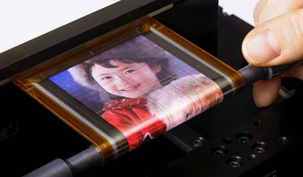
 Flexible")

6 Technological interest Low processing T (< 200ºC) Flexible Huge variety of polymers / organic molecules

7 Dyes Pigments: stables, small-molecule, visible optical absorption

8 Molecules with adjustable properties
")
 (Gate) Light")

9 Organic Devices Thin-film transistor (TFT) Thin-Film (Drain) (Source) (Gate) Light emitter diode (OLED) Solar cell Metal Electrodes Transparent electrode
10 Organic Solar Cells
11
12
13 Organic material (or molecular material)?

14 Organic material (or molecular material)?

15 Polymer vs small molecule Complexity
16 Organic Solar Cells Two approach Polymer Small molecule Solution spin coating Thermal evaporation (sublimation) in high-vacuum
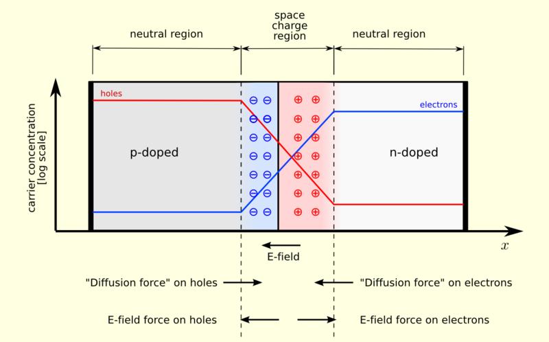
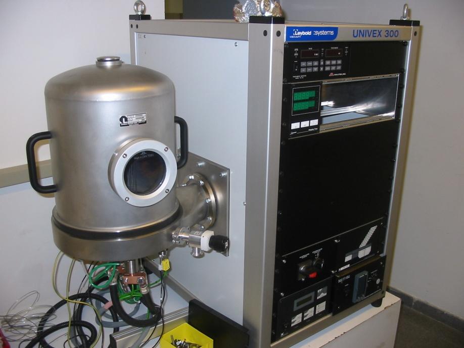
17 Basic structure Metal (Al, Ag) Organic semiconductor p / n layers Glass / Plastic ITO ITO: Indium Tin Oxide / Conductor and transparent Usually deposited by Sputtering

18 Inorganic Solar cell (Crystalline silicon)
 due to the low dielectric constant Quasi-free charge carriers Frenkel exciton Charge-transfer (CT)")
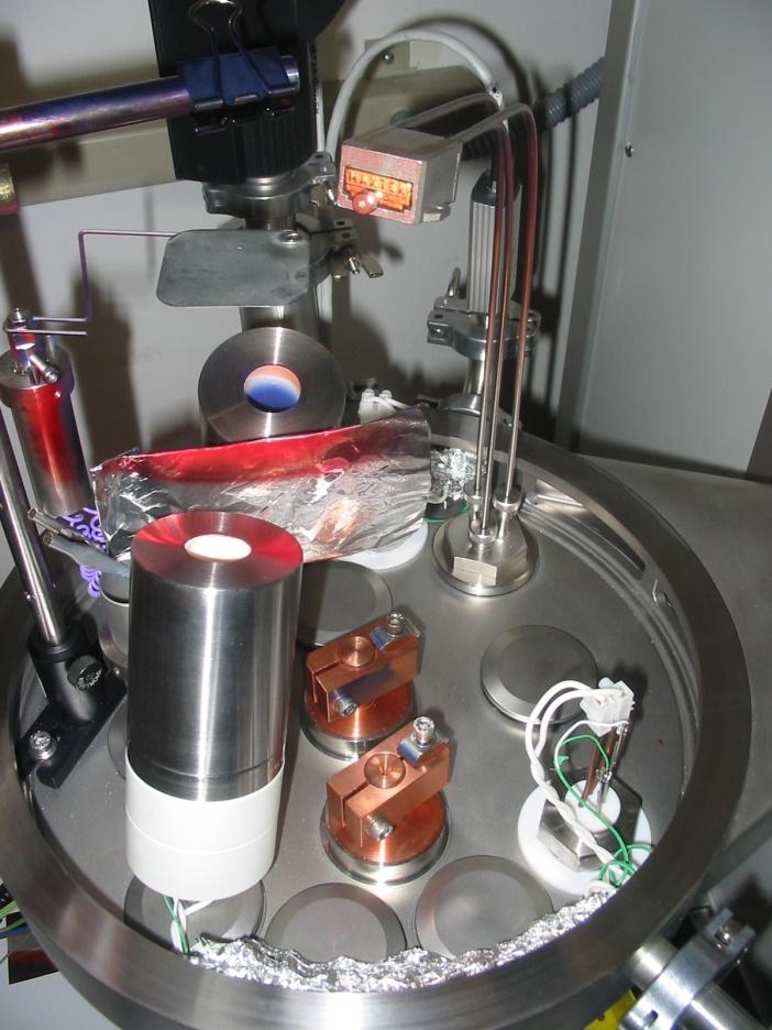
19 Exciton Exciton: electron - hole pair (molecular or Frenkel exciton) quasi-free Frenkel CT F = - e 2 /4 π εε 0 r 2 Large binding energy (>> kt) due to the low dielectric constant Quasi-free charge carriers Frenkel exciton Charge-transfer (CT) exciton

20 HOMO LUMO levels LUMO Low Unocupied Molecular Orbital HOMO High Occupied Molecular Orbital LUMO similar to conduction band HOMO similar to valence band IP Ionization Potential [remove electron] EA Electron affinity [energy gained when an electron is added].
21 Photocurrent generation 1 Photon absorption and exciton generation 2 Exciton diffusion 3 Charge Transfer 4 Carrier collection anode cathode Donor Acceptor Donor Acceptor Semiconductor P-type Semiconductor N-type

")

")
22 Polymer solar cell Semiconductor Dissolution (different solvent) Spin coating Liquid distribution (spin-coating, or Dr Blade technique) Dr Blade technique


23 Small molecule solar cell Semiconductor (powder) Thermal evaporation in high vacuum
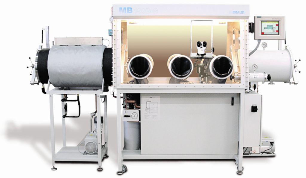
24 GloveBox
25 Our research activities at UPC on Organic Solar cells


26 Evolution Year 2002 Year 2006 Year 2011 MNT Micro and Nanotechnology group
27 Thermal evaporation MNT Micro and Nanotechnology group

28 p-type Metal evaporation n-type Organic evaporation intrinsic


29 Organic semiconductor purification by gradient thermal sublimation


30 AFM and STM microscope UHV. Small-molecule thermal deposition

 MoO3 Transparent conductive layer")
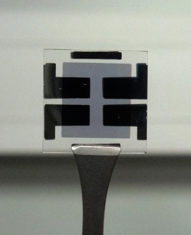
31 Our solar cell p-i-n Absorbing layer Electrode N-type Electrode P-type Font electrode (Al) BCP Absorbing layer (DBP:C 70 ) MoO3 Transparent conductive layer (ITO) glass
 Temp (C) PCE (%) Voc (V) J SC (ma/cm 2 ) 30 1.92 0.79-5.29 0.46 60 2.48 0.89-4.79 0.58 90 1.96 0.85-4.53 0.51 120 1.98 0.83-4.56 0.")
32 Bilayer solar cell Al BCP 8nm C70 40nm DBP 10nm MoO3 3nm ITO Current Density (ma/cm 2 ) DBP Substrate temperature ,0 0,2 0,4 0,6 0,8 1,0 Voltage (V) Temp (C) PCE (%) Voc (V) J SC (ma/cm 2 ) FF
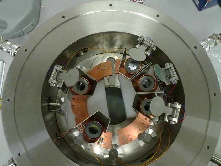
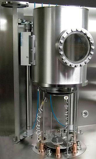
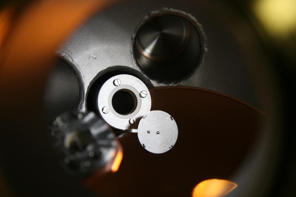
33 Facilities
34 Coevaporated solar cell Al BCP 8nm DBP : C70 (1:1) 40nm MoO3 3nm ITO T SUBS = 60 o C Coevaporated ~ 4% Current density (ma/cm 2 ) Jsc=11.2mA/cm 2 Voc=0.81V FF=43% η=3.93% -15-1,0-0,5 0,0 0,5 1,0 Voltage(V) Macko J.A., Lunt R.R., Osedach T.P., Brown P.R., Barr M.C., Gleason K.K., Bulovic V., Phys. Chem. Chem. Phys. 14, (2012) X. Xiao, J. D. Zimmerman, B. E. Lassiter, K. J. Bergemann, S. R. Forrest, Appl. Phys. Lett. 102, (2013)
35 Organic Thin-Film Transistors (OTFTs)
36 Working principle TFTs V Positive application GS Current D V DS Positive application S N-type Semiconductor _ G Dielectric
37 Working principle TFTs V GS Negative application Current V DS Negative application D S N-type Semiconductor G Dielectric
 DP-PTCDI F16CuPc PTCDI-C 13 TTF-TCNQ MNT Micro and")
38 OTFTs OTFTs allows to determine field-effect mobility (µ) µ is an important parameter in organic solar cells OTFTs allow to optimize technological parameters P-type N-type N N N N N Cu N N N pentacene CuPc Carbazole Picene fullerene (C 60 ) DP-PTCDI F16CuPc PTCDI-C 13 TTF-TCNQ MNT Micro and Nanotechnology group


39 TFTs Structure Au Drain & Source electrodes Organic semiconductor Active layer SiO 2 Insulator c-si (Gate electrode)
 V DS = -10V -80-60 -40-20 0 20 Gate-Source Voltage (V) µ = 0.5 cm 2 /V s V T = 15.6 V µ = 0.036 cm 2 /V s V T = 61.")
40 Individual TFT characteristics Drain-Source Current (A) Drain-Source Current (A) 0-1x x x10-5 Pentacene PTCDI-C 13 V GS = -16, -32, -48, -64 V -4x Drain-Source Voltage (V) V DS = -10V Gate-Source Voltage (V) µ = 0.5 cm 2 /V s V T = 15.6 V µ = cm 2 /V s V T = 61.7V
 60 40 20 0-20 -40 I DS (na) 0-2 -4-6 -8 V")
 T subs = 30 ºC T subs = 60 ºC -60-40")

 Pentacene PMMA (gate")
41 OTFTs on alumnium foil W L Dielectric PMMA I DS (na) I DS (na) V GS =-20 V V GS =-30 V V GS =-40 V V DS (V) T subs = 30 ºC T subs = 60 ºC V DS (V) T subs = 90 ºC V GS = -40 V J. Puigdollers et al., presented at MRS Spring Meeting 2005 Au contacts (Source/Drain) Pentacene PMMA (gate dielectric) Al foil (gate electrode)


42 Complementary Inverter V DD G S V DD p-channel V IN V OUT V IN D D V OUT G S n-channel V SS V SS pentacene V OUT O PTCDI C 13 H 27 O V DD S p D n,p C 13 H 27 N O O N C 13 H 27 V SS S n V IN SiO 2 G n,p Substrate (c-si)
43 Voltage transfer characteristics V OUT Voltage Transfer Characteristics V IN V DD S G p-channel D V D OUT n-channel G S V SS Gain Gain dv OUT /dv IN V IN V in Difficulty to fabricate inverters with symmetrical characteristics
44 Complementary organic inverters (different W/L) V out n-6p 3n-4p 5n-2p V in V in Gain dv OUT /dv IN V DD V IN V OUT V SS Aspect ratio (W :W ): P N V DD 6:1 5:2 p-channel 4:3 3:4 2:5 V IN V OUT n-channel W L 1:6 V SS p-type: Pentacene n-type: PTCDI-C 13
45 Thank you
Planar Organic Photovoltaic Device. Saiful I. Khondaker
 Planar Organic Photovoltaic Device Saiful I. Khondaker Nanoscience Technology Center and Department of Physics University of Central Florida http://www.physics.ucf.edu/~khondaker W Metal 1 L ch Metal 2
Enhancing the Performance of Organic Thin-Film Transistor using a Buffer Layer
 Proceedings of the 9th International Conference on Properties and Applications of Dielectric Materials July 19-23, 29, Harbin, China L-7 Enhancing the Performance of Organic Thin-Film Transistor using
Semiconductor Polymer
 Semiconductor Polymer Organic Semiconductor for Flexible Electronics Introduction: An organic semiconductor is an organic compound that possesses similar properties to inorganic semiconductors with hole
Mesoporous titanium dioxide electrolyte bulk heterojunction
 Mesoporous titanium dioxide electrolyte bulk heterojunction The term "bulk heterojunction" is used to describe a heterojunction composed of two different materials acting as electron- and a hole- transporters,
Halbleiter Prof. Yong Lei Prof. Thomas Hannappel
 Halbleiter Prof. Yong Lei Prof. Thomas Hannappel yong.lei@tu-ilmenau.de thomas.hannappel@tu-ilmenau.de http://www.tu-ilmenau.de/nanostruk/ Organic Semiconductors & Organic Electronics Organic semiconductors
High Performance, Low Operating Voltage n-type Organic Field Effect Transistor Based on Inorganic-Organic Bilayer Dielectric System
 Journal of Physics: Conference Series PAPER OPEN ACCESS High Performance, Low Operating Voltage n-type Organic Field Effect Transistor Based on Inorganic-Organic Bilayer Dielectric System To cite this
Organic solar cells. State of the art and outlooks. Gilles Horowitz LPICM, UMR7647 CNRS - Ecole Polytechnique
 Organic solar cells. State of the art and outlooks Gilles Horowitz LPICM, UMR7647 CNRS - Ecole Polytechnique Solar energy Solar energy on earth: 75,000 tep/year 6000 times the world consumption in 2007
Flexible Organic Photovoltaics Employ laser produced metal nanoparticles into the absorption layer 1. An Introduction
 Flexible Organic Photovoltaics Employ laser produced metal nanoparticles into the absorption layer 1. An Introduction Among the renewable energy sources that are called to satisfy the continuously increased
Organic Solar Cells. All Organic solar cell. Dye-sensitized solar cell. Dye. τ inj. τ c. τ r surface states D*/D + V o I 3 D/D.
 The 4th U.S.-Korea NanoForum April 26-27, 2007, Honolulu, USA Improvement of Device Efficiency in Conjugated Polymer/Fullerene NanoComposite Solar Cells School of Semiconductor & Chemical Engineering *
e - Galvanic Cell 1. Voltage Sources 1.1 Polymer Electrolyte Membrane (PEM) Fuel Cell
 Fuel Cell") Galvanic cells convert different forms of energy (chemical fuel, sunlight, mechanical pressure, etc.) into electrical energy and heat. In this lecture, we are interested in some examples of galvanic cells.
Galvanic cells convert different forms of energy (chemical fuel, sunlight, mechanical pressure, etc.) into electrical energy and heat. In this lecture, we are interested in some examples of galvanic cells.
Supporting Information
 Electronic Supplementary Material (ESI) for Journal of Materials Chemistry A. This journal is The Royal Society of Chemistry 2018 Supporting Information A minimal non-radiative recombination loss for efficient
MASTER THESIS WORK. Study about the performance of Small Molecule Organic Solar Cells, Fabricated Based on Bulk-Hetrojunction and PIN-Junction
 MSc in Photonics Universitat Politècnica de Catalunya (UPC) Universitat Autònoma de Barcelona (UAB) Universitat de Barcelona (UB) Institut de Ciències Fotòniques (ICFO) PHOTONICSBCN http://www.photonicsbcn.eu
Supporting Information
 Supporting Information Oh et al. 10.1073/pnas.0811923106 SI Text Hysteresis of BPE-PTCDI MW-TFTs. Fig. S9 represents bidirectional transfer plots at V DS 100VinN 2 atmosphere for transistors constructed
Photovoltaics. Lecture 7 Organic Thin Film Solar Cells Photonics - Spring 2017 dr inż. Aleksander Urbaniak
 Photovoltaics Lecture 7 Organic Thin Film Solar Cells Photonics - Spring 2017 dr inż. Aleksander Urbaniak Barcelona, Spain Perpignan train station, France source: pinterest Why organic solar cells? 1.
Novel Soft Materials: Organic Semiconductors
 JSPS Science Dialogue Novel Soft Materials: Organic Semiconductors X.T. HAO Prof. UENO s Lab Faculty of Engineering, Chiba University 21 st Century Center of Excellence Program The route to research Transparent
Introduction to Organic Solar Cells
 Introduction to Organic Solar Cells Dr Chris Fell Solar Group Leader CSIRO Energy Technology, Newcastle, Australia Organic semiconductors Conductivity in polyacetylene 1970s Nobel Prize Alan J. Heeger
Section 12: Intro to Devices
 Section 12: Intro to Devices Extensive reading materials on reserve, including Robert F. Pierret, Semiconductor Device Fundamentals EE143 Ali Javey Bond Model of Electrons and Holes Si Si Si Si Si Si Si
Towards a deeper understanding of polymer solar cells
 Towards a deeper understanding of polymer solar cells Jan Anton Koster Valentin Mihailetchi Prof. Paul Blom Molecular Electronics Zernike Institute for Advanced Materials and DPI University of Groningen
High speed vacuum deposition of organic TFTs in a roll-to-roll facility
 High speed vacuum deposition of organic TFTs in a roll-to-roll facility Dr Hazel Assender University of Oxford 1 Prof Martin Taylor Eifion Patchett, Aled Williams Prof Long Lin Prof Steve Yeates Dr John
SUPPLEMENTARY INFORMATION
 Supplementary Information Efficient inorganic-organic hybrid heterojunction solar cells containing perovskite compound and polymeric hole conductors Jin Hyuck Heo, Sang Hyuk Im, Jun Hong Noh, Tarak N.
Introducing the RoVaCBE Flagship project: Roll-to-roll Vacuum-processed Carbon Based Electronics. Dr Hazel Assender, University of Oxford
 Introducing the RoVaCBE Flagship project: Roll-to-roll Vacuum-processed Carbon Based Electronics Dr Hazel Assender, University of Oxford DALMATIAN TECHNOLOGY 21 st Sept 2010 1 Organic electronics Opportunity
Organic Electronic Devices
 Organic Electronic Devices Week 4: Organic Photovoltaic Devices Lecture 4.1: Overview of Organic Photovoltaic Devices Bryan W. Boudouris Chemical Engineering Purdue University 1 Lecture Overview and Learning
ESE370: Circuit-Level Modeling, Design, and Optimization for Digital Systems
 ESE370: Circuit-Level Modeling, Design, and Optimization for Digital Systems Lec 6: September 14, 2015 MOS Model You are Here: Transistor Edition! Previously: simple models (0 and 1 st order) " Comfortable
Initial Stages of Growth of Organic Semiconductors on Graphene
 Initial Stages of Growth of Organic Semiconductors on Graphene Presented by: Manisha Chhikara Supervisor: Prof. Dr. Gvido Bratina University of Nova Gorica Outline Introduction to Graphene Fabrication
Low-bandgap small molecules for near-infrared photovoltaic applications
 Low-bandgap small molecules for near-infrared photovoltaic applications M. Ballarotto W.N. Herman D.B. Romero Low-bandgap small molecules for near-infrared photovoltaic applications M. Ballarotto, a,b
Electronic Supplementary Information (ESI)
") Electronic Supplementary Material (ESI) for Journal of Materials Chemistry A. This journal is The Royal Society of Chemistry 2018 Electronic Supplementary Information (ESI) Sifting α,ω-di(thiophen-2-yl)alkanes
Electronic Supplementary Material (ESI) for Journal of Materials Chemistry A. This journal is The Royal Society of Chemistry 2018 Electronic Supplementary Information (ESI) Sifting α,ω-di(thiophen-2-yl)alkanes
EIT KIC InnoEnergy Master s Programme. Renewable Energy - RENE
 EIT KIC InnoEnergy Master s Programme Renewable Energy - RENE MSc Thesis Fabrication and Characterization of Small Molecule Organic Solar Cells Author: Mulugeta Ayele Birhanu Principal supervisor: Dr.
Supplementary Figures
 Supplementary Figures Supplementary Figure 1 Measured versus calculated optical transitions in the CPX. The UV/Vis/NIR spectrum obtained experimentally for the 1:1 blend of 4T and F4TCNQ (red curve) is
Real-time and in-line Optical monitoring of Functional Nano-Layer Deposition on Flexible Polymeric Substrates
 Real-time and in-line Optical monitoring of Functional Nano-Layer Deposition on Flexible Polymeric Substrates S. Logothetidis Lab for Thin Films, Nanosystems & Nanometrology, Aristotle University of Thessaloniki,
Numerical model of planar heterojunction organic solar cells
 Article Materials Science July 2011 Vol.56 No.19: 2050 2054 doi: 10.1007/s11434-011-4376-4 SPECIAL TOPICS: Numerical model of planar heterojunction organic solar cells MA ChaoZhu 1 PENG YingQuan 12* WANG
Structure Property Relationships of. Organic Light-Emitting Diodes. Michael Kochanek May 19, 2006 MS&E 542 Flexible Electronics
 Structure Property Relationships of Organic Light-Emitting Diodes Michael Kochanek May 19, 2006 MS&E 542 Flexible Electronics Introduction Many of today s solid-state inorganic microelectronic devices
Triplet state diffusion in organometallic and organic semiconductors
 Triplet state diffusion in organometallic and organic semiconductors Prof. Anna Köhler Experimental Physik II University of Bayreuth Germany From materials properties To device applications Organic semiconductors
Organic LEDs part 6. Exciton Recombination Region in Organic LEDs. Handout: Bulovic, et al., Chem. Phys. Lett. 287, 455 (1998); 308, 317 (1999).
; 308, 317 (1999).") Organic LEDs part 6 Exciton Recombination Region in Organic LEDs White OLED Flexible OLEDs Solvation Effect Solid State Solvation Handout: Bulovic, et al., Chem. Phys. Lett. 287, 455 (1998); 308, 317 (1999).
Organic LEDs part 6 Exciton Recombination Region in Organic LEDs White OLED Flexible OLEDs Solvation Effect Solid State Solvation Handout: Bulovic, et al., Chem. Phys. Lett. 287, 455 (1998); 308, 317 (1999).
Organic Electronic Devices
 Organic Electronic Devices Week 5: Organic Light-Emitting Devices and Emerging Technologies Lecture 5.5: Course Review and Summary Bryan W. Boudouris Chemical Engineering Purdue University 1 Understanding
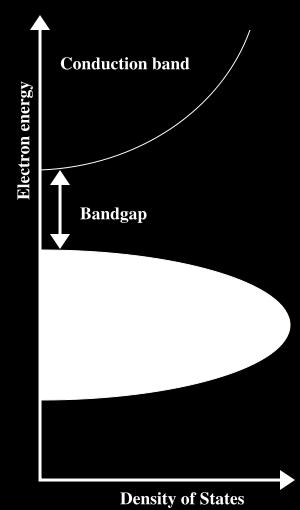
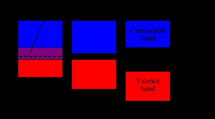
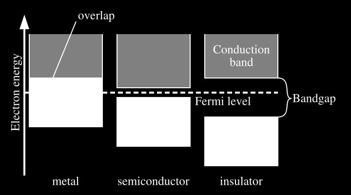
Classification of Solids
 Classification of Solids Classification by conductivity, which is related to the band structure: (Filled bands are shown dark; D(E) = Density of states) Class Electron Density Density of States D(E) Examples
Supporting Information
 Supporting Information Enhanced Thermal Stability in Perovskite Solar Cells by Assembling 2D/3D Stacking Structures Yun Lin 1, Yang Bai 1, Yanjun Fang 1, Zhaolai Chen 1, Shuang Yang 1, Xiaopeng Zheng 1,
Surface Transfer Doping of Diamond by Organic Molecules
 Surface Transfer Doping of Diamond by Organic Molecules Qi Dongchen Department of Physics National University of Singapore Supervisor: Prof. Andrew T. S. Wee Dr. Gao Xingyu Scope of presentation Overview
Mini-project report. Organic Photovoltaics. Rob Raine
 Mini-project report Organic Photovoltaics Rob Raine dtp11rdr@sheffield.ac.uk 10/2/2012 ASSIGNMENT COVER SHEET 2010/2011 A completed copy of this sheet MUST be attached to coursework contributing towards
Extensive reading materials on reserve, including
 Section 12: Intro to Devices Extensive reading materials on reserve, including Robert F. Pierret, Semiconductor Device Fundamentals EE143 Ali Javey Bond Model of Electrons and Holes Si Si Si Si Si Si Si
Nanotechnology and Solar Energy. Solar Electricity Photovoltaics. Fuel from the Sun Photosynthesis Biofuels Split Water Fuel Cells
 Nanotechnology and Solar Energy Solar Electricity Photovoltaics Fuel from the Sun Photosynthesis Biofuels Split Water Fuel Cells Solar cell A photon from the Sun generates an electron-hole pair in a semiconductor.
Role of Surface Chemistry on Charge Carrier Transport in Quantum Dot Solids
 Role of Surface Chemistry on Charge Carrier Transport in Quantum Dot Solids Cherie R. Kagan, University of Pennsylvania in collaboration with the Murray group Density of Electronic States in Quantum Dot
High operational stability of n-type organic transistors based on Naphthalene Bisimide
 High operational stability of n-type organic transistors based on Naphthalene Bisimide Maria C.R. de Medeiros, Izabela Tszydel 2, Tomasz Marszalek 2, 3, Malgorzata Zagorska 2, Jacek Ulanski 2, Henrique
Supporting information. and/or J -aggregation. Sergey V. Dayneko, Abby-Jo Payne and Gregory C. Welch*
 Supporting information Inverted P3HT:PC61BM organic solar cells incorporating a -extended squaraine dye with H- and/or J -aggregation. Sergey V. Dayneko, Abby-Jo Payne and Gregory C. Welch* Department
Lecture 15 OUTLINE. MOSFET structure & operation (qualitative) Review of electrostatics The (N)MOS capacitor
 Review of electrostatics The (N)MOS capacitor") Lecture 15 OUTLINE MOSFET structure & operation (qualitative) Review of electrostatics The (N)MOS capacitor Electrostatics Charge vs. voltage characteristic Reading: Chapter 6.1 6.2.1 EE15 Spring 28 Lecture
Lecture 15 OUTLINE MOSFET structure & operation (qualitative) Review of electrostatics The (N)MOS capacitor Electrostatics Charge vs. voltage characteristic Reading: Chapter 6.1 6.2.1 EE15 Spring 28 Lecture
SUPPLEMENTARY INFORMATION
 SUPPLEMENTARY INFORMATION Flexible, high-performance carbon nanotube integrated circuits Dong-ming Sun, Marina Y. Timmermans, Ying Tian, Albert G. Nasibulin, Esko I. Kauppinen, Shigeru Kishimoto, Takashi
Supporting Information
 Electronic Supplementary Material (ESI) for ChemComm. This journal is The Royal Society of Chemistry 2014 Supporting Information High-k Polymer/Graphene Oxide Dielectrics for Low-Voltage Flexible Nonvolatile
Electronic Supplementary Information. Molecular Antenna Tailored Organic Thin-film Transistor for. Sensing Application
 Electronic Supplementary Material (ESI) for Materials Horizons. This journal is The Royal Society of Chemistry 2017 Electronic Supplementary Information Molecular Antenna Tailored Organic Thin-film Transistor
A. Optimizing the growth conditions of large-scale graphene films
 1 A. Optimizing the growth conditions of large-scale graphene films Figure S1. Optical microscope images of graphene films transferred on 300 nm SiO 2 /Si substrates. a, Images of the graphene films grown
! Previously: simple models (0 and 1 st order) " Comfortable with basic functions and circuits. ! This week and next (4 lectures)
 Comfortable with basic functions and circuits. ! This week and next (4 lectures)") ESE370: CircuitLevel Modeling, Design, and Optimization for Digital Systems Lec 6: September 14, 2015 MOS Model You are Here: Transistor Edition! Previously: simple models (0 and 1 st order) " Comfortable
ESE370: CircuitLevel Modeling, Design, and Optimization for Digital Systems Lec 6: September 14, 2015 MOS Model You are Here: Transistor Edition! Previously: simple models (0 and 1 st order) " Comfortable
Effect of doping on performance of organic solar cells
 1 Effect of doping on performance of organic solar cells V. A. Trukhanov, V.V. Bruevich, D.Yu. Paraschuk International Laser Center and Faculty of Physics, M.V. Lomonosov Moscow State University, Moscow
A. OTHER JUNCTIONS B. SEMICONDUCTOR HETEROJUNCTIONS -- MOLECULES AT INTERFACES: ORGANIC PHOTOVOLTAIC BULK HETEROJUNCTION DYE-SENSITIZED SOLAR CELL
 A. OTHER JUNCTIONS B. SEMICONDUCTOR HETEROJUNCTIONS -- MOLECULES AT INTERFACES: ORGANIC PHOTOVOLTAIC BULK HETEROJUNCTION DYE-SENSITIZED SOLAR CELL February 9 and 14, 2012 The University of Toledo, Department
Introduction. Fang-Chung Chen Department of Photonics and Display Institute National Chiao Tung University. Organic light-emitting diodes
 rganic light-emitting diodes Introduction Fang-Chung Chen Department of Photonics and Display Institute National Chiao Tung University rganic light-emitting diodes --The emerging technology LED Displays
Lecture 15 OUTLINE. MOSFET structure & operation (qualitative) Review of electrostatics The (N)MOS capacitor
 Review of electrostatics The (N)MOS capacitor") Lecture 15 OUTLINE MOSFET structure & operation (qualitative) Review of electrostatics The (N)MOS capacitor Electrostatics t ti Charge vs. voltage characteristic Reading: Chapter 6.1 6.2.1 EE105 Fall 2007
Lecture 15 OUTLINE MOSFET structure & operation (qualitative) Review of electrostatics The (N)MOS capacitor Electrostatics t ti Charge vs. voltage characteristic Reading: Chapter 6.1 6.2.1 EE105 Fall 2007
Lecture 3: CMOS Transistor Theory
 Lecture 3: CMOS Transistor Theory Outline Introduction MOS Capacitor nmos I-V Characteristics pmos I-V Characteristics Gate and Diffusion Capacitance 2 Introduction So far, we have treated transistors
ESE 570: Digital Integrated Circuits and VLSI Fundamentals
 ESE 570: Digital Integrated Circuits and VLSI Fundamentals Lec 4: January 23, 2018 MOS Transistor Theory, MOS Model Penn ESE 570 Spring 2018 Khanna Lecture Outline! CMOS Process Enhancements! Semiconductor
Section 12: Intro to Devices
 Section 12: Intro to Devices Extensive reading materials on reserve, including Robert F. Pierret, Semiconductor Device Fundamentals Bond Model of Electrons and Holes Si Si Si Si Si Si Si Si Si Silicon
Organic Solar Cells Revised 5/29/ :21:06
 Organic Solar Cells Revised 5/29/2015 23:21:06 Oscar Monge Villora, Jack Thomas Parley and Pablo Ribera Manzano Universitat Politècnica de Catalunya, ETSETB, Barcelona I. INTRODUCTION Conventional solar
ESE370: Circuit-Level Modeling, Design, and Optimization for Digital Systems
 ESE370: Circuit-Level Modeling, Design, and Optimization for Digital Systems Lec 6: September 18, 2017 MOS Model You are Here: Transistor Edition! Previously: simple models (0 and 1 st order) " Comfortable
Characterization of Small Molecule Organic Solar Cells by Variable Light Intensity Measurements
 Characterization of Small Molecule Organic Solar Cells by ariable Light Intensity Measurements Resumen Treball Final - Màster Interuniversitari UB-UPC d Enginyeria en Energia - Convocatòria: Mayo 213 Alumne:
EE 5211 Analog Integrated Circuit Design. Hua Tang Fall 2012
 EE 5211 Analog Integrated Circuit Design Hua Tang Fall 2012 Today s topic: 1. Introduction to Analog IC 2. IC Manufacturing (Chapter 2) Introduction What is Integrated Circuit (IC) vs discrete circuits?
Physics of Organic Semiconductor Devices: Materials, Fundamentals, Technologies and Applications
 Physics of Organic Semiconductor Devices: Materials, Fundamentals, Technologies and Applications Dr. Alex Zakhidov Assistant Professor, Physics Department Core faculty at Materials Science, Engineering
ORGANIC SEMICONDUCTOR 3,4,9,10-Perylenetetracarboxylic dianhydride (PTCDA)
") ORGANIC SEMICONDUCTOR 3,4,9,10-Perylenetetracarboxylic dianhydride (PTCDA) Suvranta Tripathy Department of Physics University of Cincinnati Cincinnati, Ohio 45221 March 8, 2002 Abstract In the last decade
ORGANIC SEMICONDUCTOR 3,4,9,10-Perylenetetracarboxylic dianhydride (PTCDA) Suvranta Tripathy Department of Physics University of Cincinnati Cincinnati, Ohio 45221 March 8, 2002 Abstract In the last decade
Charge Extraction from Complex Morphologies in Bulk Heterojunctions. Michael L. Chabinyc Materials Department University of California, Santa Barbara
 Charge Extraction from Complex Morphologies in Bulk Heterojunctions Michael L. Chabinyc Materials Department University of California, Santa Barbara OPVs Vs. Inorganic Thin Film Solar Cells Alta Devices
PHOTOVOLTAICS Fundamentals
 PHOTOVOLTAICS Fundamentals PV FUNDAMENTALS Semiconductor basics pn junction Solar cell operation Design of silicon solar cell SEMICONDUCTOR BASICS Allowed energy bands Valence and conduction band Fermi
Low-temperature-processed inorganic perovskite solar cells via solvent engineering with enhanced mass transport
 Electronic Supplementary Material (ESI) for Journal of Materials Chemistry A. This journal is The Royal Society of Chemistry 1 Low-temperature-processed inorganic perovskite solar cells via solvent engineering
Photovoltaic cell and module physics and technology
 Photovoltaic cell and module physics and technology Vitezslav Benda, Prof Czech Technical University in Prague benda@fel.cvut.cz www.fel.cvut.cz 6/21/2012 1 Outlines Photovoltaic Effect Photovoltaic cell
Supplementary Figure S1. AFM images of GraNRs grown with standard growth process. Each of these pictures show GraNRs prepared independently,
 Supplementary Figure S1. AFM images of GraNRs grown with standard growth process. Each of these pictures show GraNRs prepared independently, suggesting that the results is reproducible. Supplementary Figure
EECS143 Microfabrication Technology
 EECS143 Microfabrication Technology Professor Ali Javey Introduction to Materials Lecture 1 Evolution of Devices Yesterday s Transistor (1947) Today s Transistor (2006) Why Semiconductors? Conductors e.g
Chapter 3 Engineering Science for Microsystems Design and Fabrication
 Lectures on MEMS and MICROSYSTEMS DESIGN and MANUFACTURE Chapter 3 Engineering Science for Microsystems Design and Fabrication In this Chapter, we will present overviews of the principles of physical and
Inverted top-emitting organic light-emitting diodes using transparent conductive NiO electrode
 Applied Surface Science 244 (2005) 439 443 www.elsevier.com/locate/apsusc Inverted top-emitting organic light-emitting diodes using transparent conductive NiO electrode Se-W. Park a, Jeong-M. Choi a, Eugene
Appendix 1: List of symbols
 Appendix 1: List of symbols Symbol Description MKS Units a Acceleration m/s 2 a 0 Bohr radius m A Area m 2 A* Richardson constant m/s A C Collector area m 2 A E Emitter area m 2 b Bimolecular recombination
Unit IV Semiconductors Engineering Physics
 Introduction A semiconductor is a material that has a resistivity lies between that of a conductor and an insulator. The conductivity of a semiconductor material can be varied under an external electrical
Solar Cells Utilizing Small Molecular Weight Organic Semiconductors
 PROGRESS IN PHOTOVOLTAICS: RESEARCH AND APPLICATIONS Prog. Photovolt: Res. Appl. 2007; 15:659 676 Published online 24 October 2007 in Wiley InterScience (www.interscience.wiley.com)..788 Special Issue
Spring Semester 2012 Final Exam
 Spring Semester 2012 Final Exam Note: Show your work, underline results, and always show units. Official exam time: 2.0 hours; an extension of at least 1.0 hour will be granted to anyone. Materials parameters
Conjugated Polymers Based on Benzodithiophene for Organic Solar Cells. Wei You
 Wake Forest Nanotechnology Conference October 19, 2009 Conjugated Polymers Based on Benzodithiophene for Organic olar Cells Wei You Department of Chemistry and Institute for Advanced Materials, Nanoscience
Digital Electronics Part II - Circuits
 Digital Electronics Part - Circuits Dr.. J. Wassell Gates from Transistors ntroduction Logic circuits are non-linear, consequently we will introduce a graphical technique for analysing such circuits The
smal band gap Saturday, April 9, 2011
 small band gap upper (conduction) band empty small gap valence band filled 2s 2p 2s 2p hybrid (s+p)band 2p no gap 2s (depend on the crystallographic orientation) extrinsic semiconductor semi-metal electron
1 Name: Student number: DEPARTMENT OF PHYSICS AND PHYSICAL OCEANOGRAPHY MEMORIAL UNIVERSITY OF NEWFOUNDLAND. Fall :00-11:00
 1 Name: DEPARTMENT OF PHYSICS AND PHYSICAL OCEANOGRAPHY MEMORIAL UNIVERSITY OF NEWFOUNDLAND Final Exam Physics 3000 December 11, 2012 Fall 2012 9:00-11:00 INSTRUCTIONS: 1. Answer all seven (7) questions.
Supporting Information
 Electronic Supplementary Material (ESI) for Nanoscale. This journal is The Royal Society of Chemistry 215 Supporting Information Enhanced Photovoltaic Performances of Graphene/Si Solar Cells by Insertion
Copper(I) thiocyanate (CuSCN) as a hole-transport material for large-area opto/electronics
 thiocyanate (CuSCN) as a hole-transport material for large-area opto/electronics") TOPICAL REVIEW Copper(I) thiocyanate (CuSCN) as a hole-transport material for large-area opto/electronics Nilushi Wijeyasinghe and Thomas D. Anthopoulos Department of Physics and Centre for Plastic Electronics,
TOPICAL REVIEW Copper(I) thiocyanate (CuSCN) as a hole-transport material for large-area opto/electronics Nilushi Wijeyasinghe and Thomas D. Anthopoulos Department of Physics and Centre for Plastic Electronics,
Vikram Kuppa School of Energy, Environmental, Biological and Medical Engineering College of Engineering and Applied Science University of Cincinnati
 Vikram Kuppa School of Energy, Environmental, Biological and Medical Engineering College of Engineering and Applied Science University of Cincinnati vikram.kuppa@uc.edu Fei Yu Yan Jin Andrew Mulderig Greg
MOSFET: Introduction
 E&CE 437 Integrated VLSI Systems MOS Transistor 1 of 30 MOSFET: Introduction Metal oxide semiconductor field effect transistor (MOSFET) or MOS is widely used for implementing digital designs Its major
REDUCED GRAPHITE OXIDE-INDIUM TIN OXIDE COMPOSITES FOR TRANSPARENT ELECTRODE USING SOLUTION PROCESS
 18 TH INTERNATIONAL CONFERENCE ON COMPOSITE MATERIALS REDUCED GRAPHITE OXIDE-INDIUM TIN OXIDE COMPOSITES FOR TRANSPARENT ELECTRODE USING SOLUTION PROCESS K. S. Choi, Y. Park, K-.C. Kwon, J. Kim, C. K.
Semiconductor Detectors
 Semiconductor Detectors Summary of Last Lecture Band structure in Solids: Conduction band Conduction band thermal conductivity: E g > 5 ev Valence band Insulator Charge carrier in conductor: e - Charge
electronics ISSN
 Electronics 2014, 3, 351-380; doi:10.3390/electronics3020351 Review OPEN ACCESS electronics ISSN 2079-9292 www.mdpi.com/journal/electronics Bandgap Science for Organic Solar Cells Masahiro Hiramoto 1,2,
EECS130 Integrated Circuit Devices
 EECS130 Integrated Circuit Devices Professor Ali Javey 8/30/2007 Semiconductor Fundamentals Lecture 2 Read: Chapters 1 and 2 Last Lecture: Energy Band Diagram Conduction band E c E g Band gap E v Valence
Synthesis Breakout. Overarching Issues
 Synthesis Breakout. Overarching Issues 1. What are fundamental structural and electronic factors limiting Jsc, Voc, and FF in typical polymer bulk-heterojunction cells? Rational P- and N-type materials
E L E C T R O P H O S P H O R E S C E N C E
 Organic LEDs part 4 E L E C T R O P H O S P H O R E S C E C E. OLED efficiency 2. Spin 3. Energy transfer 4. Organic phosphors 5. Singlet/triplet ratios 6. Phosphor sensitized fluorescence 7. Endothermic
Electronic Supplementary Information. Yunlong Guo, Chao Liu, Kento Inoue, Koji Harano, Hideyuki Tanaka,* and Eiichi Nakamura*
 Electronic Supplementary Material (ESI) for Journal of Materials Chemistry A. This journal is The Royal Society of Chemistry 2014 Electronic Supplementary Information Enhancement in the efficiency of an
A. K. Das Department of Physics, P. K. College, Contai; Contai , India.
 IOSR Journal of Applied Physics (IOSR-JAP) e-issn: 2278-4861.Volume 7, Issue 2 Ver. II (Mar. - Apr. 2015), PP 08-15 www.iosrjournals.org Efficiency Improvement of p-i-n Structure over p-n Structure and
EE143 Fall 2016 Microfabrication Technologies. Evolution of Devices
 EE143 Fall 2016 Microfabrication Technologies Prof. Ming C. Wu wu@eecs.berkeley.edu 511 Sutardja Dai Hall (SDH) 1-1 Evolution of Devices Yesterday s Transistor (1947) Today s Transistor (2006) 1-2 1 Why
Lecture 0: Introduction
 Lecture 0: Introduction Introduction q Integrated circuits: many transistors on one chip q Very Large Scale Integration (VLSI): bucketloads! q Complementary Metal Oxide Semiconductor Fast, cheap, low power
Photoconductive Atomic Force Microscopy for Understanding Nanostructures and Device Physics of Organic Solar Cells
 Photoconductive AFM of Organic Solar Cells APP NOTE 15 Photoconductive Atomic Force Microscopy for Understanding Nanostructures and Device Physics of Organic Solar Cells Xuan-Dung Dang and Thuc-Quyen Nguyen
Keywords: thin-film transistors, organic polymers, bias temperature stress, electrical instabilities, transient regime.
 Time dependence of organic polymer thin-film transistors current Sandrine Martin *, Laurence Dassas, Michael C. Hamilton and Jerzy Kanicki University of Michigan, Solid-State Electronics Laboratory, Department
Chemistry Instrumental Analysis Lecture 8. Chem 4631
 Chemistry 4631 Instrumental Analysis Lecture 8 UV to IR Components of Optical Basic components of spectroscopic instruments: stable source of radiant energy transparent container to hold sample device
BASIC CONCEPTS on ORGANIC SEMICONDUCTORS. Marco Sampietro COURSE OVERVIEW
 Advanced Course on ORGANIC ELECRONICS Principles, devices and applications BASIC CONCEPTS on ORGANIC SEMICONDUCTORS Marco Sampietro 1 Basics on Organic Devices COURSE OVERVIEW How the organic semiconductor
FYS 3028/8028 Solar Energy and Energy Storage. Calculator with empty memory Language dictionaries
 Faculty of Science and Technology Exam in: FYS 3028/8028 Solar Energy and Energy Storage Date: 11.05.2016 Time: 9-13 Place: Åsgårdvegen 9 Approved aids: Type of sheets (sqares/lines): Number of pages incl.
Characterization of electric charge carrier transport in organic semiconductors by time-of-flight technique
 Characterization of electric charge carrier transport in organic semiconductors by time-of-flight technique Raveendra Babu Penumala Mentor: Prof. dr. Gvido Bratina Laboratory of Organic Matter Physics
Research Article Modeling and Optimization of Advanced Single- and Multijunction Solar Cells Based on Thin-Film a-si:h/sige Heterostructure
 International Scholarly Research Network ISRN Renewable Energy Volume 211, Article ID 712872, 8 pages doi:1.542/211/712872 Research Article Modeling and Optimization of Advanced Single- and Multijunction
! Previously: simple models (0 and 1 st order) " Comfortable with basic functions and circuits. ! This week and next (4 lectures)
 Comfortable with basic functions and circuits. ! This week and next (4 lectures)") ESE370: CircuitLevel Modeling, Design, and Optimization for Digital Systems Lec 6: September 18, 2017 MOS Model You are Here: Transistor Edition! Previously: simple models (0 and 1 st order) " Comfortable
ESE370: CircuitLevel Modeling, Design, and Optimization for Digital Systems Lec 6: September 18, 2017 MOS Model You are Here: Transistor Edition! Previously: simple models (0 and 1 st order) " Comfortable