Initial Stages of Growth of Organic Semiconductors on Graphene
|
|
|
- Garry Nicholson
- 5 years ago
- Views:
Transcription

1 Initial Stages of Growth of Organic Semiconductors on Graphene Presented by: Manisha Chhikara Supervisor: Prof. Dr. Gvido Bratina University of Nova Gorica
2 Outline Introduction to Graphene Fabrication Characterization: AFM (Atomic Force Microscope) Properties: Electronic, Optical Applications Growth of organic semiconductors (OS) on Graphene OMBD (Organic Molecular Beam Deposition) Growth Modes: Types Conclusions
 Strong Flexible High intrinsic carrier mobility ~ 200000 cm 2 /Vs High thermal conductivity Graphene Carbon nanotubes")
3 Introduction to Graphene Hexagonal arrangement of carbon atoms forming an atom thick planar sheets Graphite C-C bond ~ 1.42 Å Thickness of one 1 atomic layer ~.34nm (~ layer spacing of graphite) Strong Flexible High intrinsic carrier mobility ~ cm 2 /Vs High thermal conductivity Graphene Carbon nanotubes Fullerene


4 Graphene monolayer in great minority among thicker flakes Unlike nanotubes, no clear signature by TEM Completely transparent on most of substrates The only method: AFM very low throughput at high resolution Late discovery of Graphene Discovered in µm

5 The Nobel Prize in Physics 2010 Graphene Andre Geim Konstantin Novoselov
6 Impact of graphene in Scientific community Citations Publications 2,000 1,500 1,000 5, ,000 40,000 30,000 20,000 10,

7 Fabrication Methods: Mechanical exfoliation Advantages: Cheap Limitations: Limited to small area Many uneven films Time consuming


8 Chemical vapor deposition (CVD) method Advantages: Great technique for large area graphene Requires less labor Continuous films Limitation: Require high temperature

9 Band Structure of graphene The spectrum is described by the tight-binding Hamiltonian on a hexagonal lattice Band crossing at K and K (Dirac points) Dispersion is similar to that of relativistic particles, E = hv F k Fermi velocity v F = 10 6 m /s Zero band gap semiconductor Charge carriers ~ massless Dirac Fermions
10 Absorption of light by 2D Dirac fermions Optical properties of graphene Graphene absorbs πα 2.3% of white light, where α = fine structure constant Transmission, T = 1- πα, Reflection, R<<1
 Alternative")
")

11 Possible applications of graphene TCO (Transparent conducting electrode) Alternative to ITO ( expensive, difficult to recycle) Electrode very thin (couple of nm thick) Compatible with large scale manufacturing methods Can be used to polarize light Graphene Transister Saturable absorber


12 Characterization of graphene AFM (Atomic Force Microscope) Used to characterize the surfaces on nanometer scale The force acting on the cantilever, F = -kz k = spring constant of cantilever z = deflection of cantilever Fig. Scheme illustrating the working of AFM
13 Operating modes Contact mode S~ few nm F ~10-8 to 10-6 N High resolution Non-contact mode S ~ 10 nm F ~ N Suitable for soft samples S = distance between tip and surface F = force between tip and surface


14 nm nm AFM image of graphene ~0.35 nm AFM measurement across a wrinkle confirming interlayer spacing of ~0.35 nm.
 reached charge carrier mobility of the order of 1 cm 2 /Vs Graphene can be used as a")
15 Growth of OS on graphene Low cost, mechanically flexible, easy to fabricate Aspects of interface Organic Solar cell, OLEDs, OTFTs OTFT Pentacene-based organic thin film transistors (OTFTs) reached charge carrier mobility of the order of 1 cm 2 /Vs Graphene can be used as a substrate
16 Pentacene Crystal structure - Triclinic Band gap - 2.2eV High carrier mobility Excellent interface properties with organic materials Form highly ordered organic films Structural formula of Pentacene
17 Organic Molecular Beam Deposition The growth is controlled with the precision of a single molecular layer Generation of the molecular beam Mixing zone Growth on substrate Sticking coefficient, s = N adh / N tot N adh = no. of atoms adhering to substrate N tot = no. of atoms arriving Quartz thickness monitor Sample holder Main shutter Shutter Effusion cell Fig. Organic Molecular Beam Setup
 Surface migration and dissociation of adsorbed molecules 3) Incorporation of constituent atoms into crystal lattice 4) Desorption 1 1 4 3")
18 Practically, s <1 A series of process occur 1) Adsorption of atoms or molecules impinging on substrate surface a) Physical adsorption- no electron transfer b) Chemical adsorption-electron transfer 2) Surface migration and dissociation of adsorbed molecules 3) Incorporation of constituent atoms into crystal lattice 4) Desorption
19 Structure of organic films grown depends upon Type of molecule/substrate interaction Layer-by-layer (Frank van der Merwe) growth mode if molecule/substrate interaction > intermolecular interaction Layer-plus-island (Stranski- Krastanov)- intermediate mode layer growth unfavorable after first few layers Islands (Volmer- Weber growth mode) if intermolecular interaction > molecule/substrate Substrate temperature Density of surface defects Surface energy
20 J. A. Venables et. al, Rep. Prog. Phys 47, 399 (1984)
21 Density of islands depends upon Deposition rate Substrate temperature and described as power law p = critical exponent, K B = Boltzmann constant E nucl = activation energy for homogenous nucleation a) Surface diffusion (E d ) b) Desorption from substrate surface (E a ) c) Formation of island of critical size i with binding energy E i
 Strongly interacting surface-limited diffusion Size of the molecules Multiple")
22 Specific issues to organic thin film growth Internal degrees of freedom Orientational degrees of freedomorientation domain Vibrational degrees of freedom-impact on interaction with surface Interaction potential (Molecule-molecule and moleculesubstrate) Strongly interacting surface-limited diffusion Size of the molecules Multiple domains-disorder
 Pentacene evaporated from fused quartz crucible Film thickness, 0.5nm Base pressure ~ 10-7 mbar Substrate temperature, T s ~ 338K Deposition rate ~ 0.")
23 Experimental details: Example 1: Pentacene on SiO 2 Si wafer with 200nm thick SiO 2 layer( roughness < 0.1nm) Pentacene evaporated from fused quartz crucible Film thickness, 0.5nm Base pressure ~ 10-7 mbar Substrate temperature, T s ~ 338K Deposition rate ~ 0.45nm/min S. Pratontep et.al, PRB 689,165201(2004)
24 Effect of deposition rate Morphology of island becomes compact No. density of island increases Effect of T s Density N decreases by a few orders of magnitude as T s increased from 29 C to 80 C Conclusion: Nucleation density of islands can be tuned by both deposition rate and substrate temperature S. Pratontep et.al, PRB 689,165201(2004)
 thick on different")
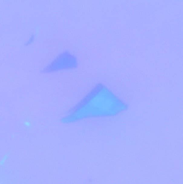
25 Example 2: AFM images of Pentacene (0.2 ML) thick on different substrates

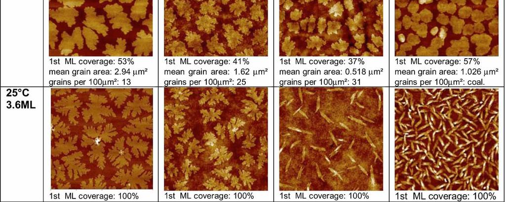
26 Pentacene on different substrates

27 Film thickness ~ 33 ML T s = 25 C Transition from 2D to 3D- island growth Conclusion: Pentacene growth on polymers is correlated critical island size for substrates b/w C is 3<i<4 Condensation is complete although reevaporation plays some role B. Stadlober et. al PRB B 74, (2006)
28 Optical microscope images of Graphene Graphene prepared by CVD method 40 µm 40 µm Graphene prepared by exfoliation 15 µm 15 µm 40 µm


29 Pentacene on Graphene SiO 2 layer on Si wafer ~ 300 nm Pentacene deposition rate ~ 0.2 Å/ s a) Untreated graphene films b) Thermally treated graphene films AFM images of pentacene films on graphene W. H. Lee et. al., J. Am. Chem. Soc., 133, 4447 (07 March 2011)
30 Conclusions Graphene is an excellent 2D structure with unusual electronic and optical properties Organic semiconductors ( OS) on substrates can be successfully grown in sub monolayer or more monolayer by OMBD AFM is an important tool to study initial stages of growth of organic semiconductor on substrates Graphene prepared by CVD and mechanical exfoliation methods can be used as a substrate
Overview. Carbon in all its forms. Background & Discovery Fabrication. Important properties. Summary & References. Overview of current research
 Graphene Prepared for Solid State Physics II Pr Dagotto Spring 2009 Laurene Tetard 03/23/09 Overview Carbon in all its forms Background & Discovery Fabrication Important properties Overview of current
Graphene films on silicon carbide (SiC) wafers supplied by Nitride Crystals, Inc.
 wafers supplied by Nitride Crystals, Inc.") 9702 Gayton Road, Suite 320, Richmond, VA 23238, USA Phone: +1 (804) 709-6696 info@nitride-crystals.com www.nitride-crystals.com Graphene films on silicon carbide (SiC) wafers supplied by Nitride Crystals,
9702 Gayton Road, Suite 320, Richmond, VA 23238, USA Phone: +1 (804) 709-6696 info@nitride-crystals.com www.nitride-crystals.com Graphene films on silicon carbide (SiC) wafers supplied by Nitride Crystals,
Graphene. Tianyu Ye November 30th, 2011
 Graphene Tianyu Ye November 30th, 2011 Outline What is graphene? How to make graphene? (Exfoliation, Epitaxial, CVD) Is it graphene? (Identification methods) Transport properties; Other properties; Applications;
Optimizing Graphene Morphology on SiC(0001)
") Optimizing Graphene Morphology on SiC(0001) James B. Hannon Rudolf M. Tromp Graphene sheets Graphene sheets can be formed into 0D,1D, 2D, and 3D structures Chemically inert Intrinsically high carrier mobility
Optimizing Graphene Morphology on SiC(0001) James B. Hannon Rudolf M. Tromp Graphene sheets Graphene sheets can be formed into 0D,1D, 2D, and 3D structures Chemically inert Intrinsically high carrier mobility
Lecture 10 Thin Film Growth
 Lecture 10 Thin Film Growth 1/76 Announcements Homework: Homework Number 2 is returned today, please pick it up from me at the end of the class. Solutions are online. Homework 3 will be set Thursday (2
Supplementary Figure 1 Experimental setup for crystal growth. Schematic drawing of the experimental setup for C 8 -BTBT crystal growth.
 Supplementary Figure 1 Experimental setup for crystal growth. Schematic drawing of the experimental setup for C 8 -BTBT crystal growth. Supplementary Figure 2 AFM study of the C 8 -BTBT crystal growth
Graphene Novel Material for Nanoelectronics
 Graphene Novel Material for Nanoelectronics Shintaro Sato Naoki Harada Daiyu Kondo Mari Ohfuchi (Manuscript received May 12, 2009) Graphene is a flat monolayer of carbon atoms with a two-dimensional honeycomb
Carbon based Nanoscale Electronics
 Carbon based Nanoscale Electronics 09 02 200802 2008 ME class Outline driving force for the carbon nanomaterial electronic properties of fullerene exploration of electronic carbon nanotube gold rush of
Optical Spectroscopies of Thin Films and Interfaces. Dietrich R. T. Zahn Institut für Physik, Technische Universität Chemnitz, Germany
 Optical Spectroscopies of Thin Films and Interfaces Dietrich R. T. Zahn Institut für Physik, Technische Universität Chemnitz, Germany 1. Introduction 2. Vibrational Spectroscopies (Raman and Infrared)
SEMICONDUCTOR GROWTH TECHNIQUES. Introduction to growth techniques (bulk, epitaxy) Basic concepts in epitaxy (MBE, MOCVD)
 Basic concepts in epitaxy (MBE, MOCVD)") SEMICONDUCTOR GROWTH TECHNIQUES Introduction to growth techniques (bulk, epitaxy) Basic concepts in epitaxy (MBE, MOCVD) Growth Processes Bulk techniques (massive semiconductors, wafers): Si, compounds
SEMICONDUCTOR GROWTH TECHNIQUES Introduction to growth techniques (bulk, epitaxy) Basic concepts in epitaxy (MBE, MOCVD) Growth Processes Bulk techniques (massive semiconductors, wafers): Si, compounds
Transient Photocurrent Measurements of Graphene Related Materials
 Transient Photocurrent Measurements of Graphene Related Materials P. Srinivasa Rao Mentor: Prof. dr. Gvido Bratina Laboratory of Organic Matter Physics University of Nova Gorica 1 Contents: 1. Electrical
A. Optimizing the growth conditions of large-scale graphene films
 1 A. Optimizing the growth conditions of large-scale graphene films Figure S1. Optical microscope images of graphene films transferred on 300 nm SiO 2 /Si substrates. a, Images of the graphene films grown
Wafer-scale fabrication of graphene
 Wafer-scale fabrication of graphene Sten Vollebregt, MSc Delft University of Technology, Delft Institute of Mircosystems and Nanotechnology Delft University of Technology Challenge the future Delft University
Transparent Electrode Applications
 Transparent Electrode Applications LCD Solar Cells Touch Screen Indium Tin Oxide (ITO) Zinc Oxide (ZnO) - High conductivity - High transparency - Resistant to environmental effects - Rare material (Indium)
Lecture 30: Kinetics of Epitaxial Growth: Surface Diffusion and
 Lecture 30: Kinetics of Epitaxial Growth: Surface Diffusion and Nucleation Today s topics Understanding the basics of epitaxial techniques used for surface growth of crystalline structures (films, or layers).
Surface atoms/molecules of a material act as an interface to its surrounding environment;
 1 Chapter 1 Thesis Overview Surface atoms/molecules of a material act as an interface to its surrounding environment; their properties are often complicated by external adsorbates/species on the surface
III-V nanostructured materials synthesized by MBE droplet epitaxy
 III-V nanostructured materials synthesized by MBE droplet epitaxy E.A. Anyebe 1, C. C. Yu 1, Q. Zhuang 1,*, B. Robinson 1, O Kolosov 1, V. Fal ko 1, R. Young 1, M Hayne 1, A. Sanchez 2, D. Hynes 2, and
Plastic Electronics. Joaquim Puigdollers.
 Plastic Electronics Joaquim Puigdollers Joaquim.puigdollers@upc.edu Nobel Prize Chemistry 2000 Origins Technological Interest First products.. MONOCROMATIC PHILIPS Today Future Technological interest Low
Conference Return Seminar- NANO2014,Moscow State University,Moscow,Russia Date: th July 2014
 Conference Return Seminar- NANO2014,Moscow State University,Moscow,Russia Date:13-1818 th July 2014 An electrochemical method for the synthesis of single and few layers graphene sheets for high temperature
Graphene The Search For Two Dimensions. Christopher Scott Friedline Arizona State University
 Graphene The Search For Two Dimensions Christopher Scott Friedline Arizona State University What Is Graphene? Single atomic layer of graphite arranged in a honeycomb crystal lattice Consists of sp 2 -bonded
Graphene FETs EE439 FINAL PROJECT. Yiwen Meng Su Ai
 Graphene FETs EE439 FINAL PROJECT Yiwen Meng Su Ai Introduction What is Graphene? An atomic-scale honeycomb lattice made of carbon atoms Before 2004, Hypothetical Carbon Structure Until 2004, physicists
GRAPHENE the first 2D crystal lattice
 GRAPHENE the first 2D crystal lattice dimensionality of carbon diamond, graphite GRAPHENE realized in 2004 (Novoselov, Science 306, 2004) carbon nanotubes fullerenes, buckyballs what s so special about
STM and graphene. W. W. Larry Pai ( 白偉武 ) Center for condensed matter sciences, National Taiwan University NTHU, 2013/05/23
 Center for condensed matter sciences, National Taiwan University NTHU, 2013/05/23") STM and graphene W. W. Larry Pai ( 白偉武 ) Center for condensed matter sciences, National Taiwan University NTHU, 2013/05/23 Why graphene is important: It is a new form of material (two dimensional, single
STM and graphene W. W. Larry Pai ( 白偉武 ) Center for condensed matter sciences, National Taiwan University NTHU, 2013/05/23 Why graphene is important: It is a new form of material (two dimensional, single
Chapter 1 Introduction
 Chapter 1 Introduction In our planet carbon forms the basis of all organic molecules which makes it the most important element of life. It is present in over 95% of the known chemical compounds overall
Hydrogenated Graphene
 Hydrogenated Graphene Stefan Heun NEST, Istituto Nanoscienze-CNR and Scuola Normale Superiore Pisa, Italy Outline Epitaxial Graphene Hydrogen Chemisorbed on Graphene Hydrogen-Intercalated Graphene Outline
Supplementary Materials for
 advances.sciencemag.org/cgi/content/full/4/3/e1701373/dc1 Supplementary Materials for Atomically thin gallium layers from solid-melt exfoliation Vidya Kochat, Atanu Samanta, Yuan Zhang, Sanjit Bhowmick,
CVD growth of Graphene. SPE ACCE presentation Carter Kittrell James M. Tour group September 9 to 11, 2014
 CVD growth of Graphene SPE ACCE presentation Carter Kittrell James M. Tour group September 9 to 11, 2014 Graphene zigzag armchair History 1500: Pencil-Is it made of lead? 1789: Graphite 1987: The first
Graphene and Carbon Nanotubes
 Graphene and Carbon Nanotubes 1 atom thick films of graphite atomic chicken wire Novoselov et al - Science 306, 666 (004) 100μm Geim s group at Manchester Novoselov et al - Nature 438, 197 (005) Kim-Stormer
Nanostructures. Lecture 13 OUTLINE
 Nanostructures MTX9100 Nanomaterials Lecture 13 OUTLINE -What is quantum confinement? - How can zero-dimensional materials be used? -What are one dimensional structures? -Why does graphene attract so much
Imaging Methods: Scanning Force Microscopy (SFM / AFM)
") Imaging Methods: Scanning Force Microscopy (SFM / AFM) The atomic force microscope (AFM) probes the surface of a sample with a sharp tip, a couple of microns long and often less than 100 Å in diameter.
Imaging Methods: Scanning Force Microscopy (SFM / AFM) The atomic force microscope (AFM) probes the surface of a sample with a sharp tip, a couple of microns long and often less than 100 Å in diameter.
& Dirac Fermion confinement Zahra Khatibi
 Graphene & Dirac Fermion confinement Zahra Khatibi 1 Outline: What is so special about Graphene? applications What is Graphene? Structure Transport properties Dirac fermions confinement Necessity External
Nanostrukturphysik (Nanostructure Physics)
") Nanostrukturphysik (Nanostructure Physics) Prof. Yong Lei & Dr. Yang Xu Fachgebiet 3D-Nanostrukturierung, Institut für Physik Contact: yong.lei@tu-ilmenau.de; yang.xu@tu-ilmenau.de Office: Unterpoerlitzer
Nanostrukturphysik (Nanostructure Physics) Prof. Yong Lei & Dr. Yang Xu Fachgebiet 3D-Nanostrukturierung, Institut für Physik Contact: yong.lei@tu-ilmenau.de; yang.xu@tu-ilmenau.de Office: Unterpoerlitzer
Seminars in Nanosystems - I
 Seminars in Nanosystems - I Winter Semester 2011/2012 Dr. Emanuela Margapoti Emanuela.Margapoti@wsi.tum.de Dr. Gregor Koblmüller Gregor.Koblmueller@wsi.tum.de Seminar Room at ZNN 1 floor Topics of the
Part II. Introduction of Graphene
 Part II. Introduction of Graphene 1 Graphene (Mother of all graphitic form) 2D honeycomb lattice Graphene 0D 1D 3D bulky bll ball Nanotube Graphite Geims et al, Nature Materials,Vol.6 183, 2007 2 History
(a) (b) Supplementary Figure 1. (a) (b) (a) Supplementary Figure 2. (a) (b) (c) (d) (e)
 (b) Supplementary Figure 1. (a) (b) (a) Supplementary Figure 2. (a) (b) (c) (d) (e)") (a) (b) Supplementary Figure 1. (a) An AFM image of the device after the formation of the contact electrodes and the top gate dielectric Al 2 O 3. (b) A line scan performed along the white dashed line
(a) (b) Supplementary Figure 1. (a) An AFM image of the device after the formation of the contact electrodes and the top gate dielectric Al 2 O 3. (b) A line scan performed along the white dashed line
Introduction to Nanotechnology Chapter 5 Carbon Nanostructures Lecture 1
 Introduction to Nanotechnology Chapter 5 Carbon Nanostructures Lecture 1 ChiiDong Chen Institute of Physics, Academia Sinica chiidong@phys.sinica.edu.tw 02 27896766 Carbon contains 6 electrons: (1s) 2,
From nanophysics research labs to cell phones. Dr. András Halbritter Department of Physics associate professor
 From nanophysics research labs to cell phones Dr. András Halbritter Department of Physics associate professor Curriculum Vitae Birth: 1976. High-school graduation: 1994. Master degree: 1999. PhD: 2003.
Novel Soft Materials: Organic Semiconductors
 JSPS Science Dialogue Novel Soft Materials: Organic Semiconductors X.T. HAO Prof. UENO s Lab Faculty of Engineering, Chiba University 21 st Century Center of Excellence Program The route to research Transparent
Carbon nanomaterials. Gavin Lawes Wayne State University.
 Carbon nanomaterials Gavin Lawes Wayne State University glawes@wayne.edu Outline 1. Carbon structures 2. Carbon nanostructures 3. Potential applications for Carbon nanostructures Periodic table from bpc.edu
Semiconductor Polymer
 Semiconductor Polymer Organic Semiconductor for Flexible Electronics Introduction: An organic semiconductor is an organic compound that possesses similar properties to inorganic semiconductors with hole
2D MBE Activities in Sheffield. I. Farrer, J. Heffernan Electronic and Electrical Engineering The University of Sheffield
 2D MBE Activities in Sheffield I. Farrer, J. Heffernan Electronic and Electrical Engineering The University of Sheffield Outline Motivation Van der Waals crystals The Transition Metal Di-Chalcogenides
Physics of Organic Semiconductor Devices: Materials, Fundamentals, Technologies and Applications
 Physics of Organic Semiconductor Devices: Materials, Fundamentals, Technologies and Applications Dr. Alex Zakhidov Assistant Professor, Physics Department Core faculty at Materials Science, Engineering
Outline. Introduction: graphene. Adsorption on graphene: - Chemisorption - Physisorption. Summary
 Outline Introduction: graphene Adsorption on graphene: - Chemisorption - Physisorption Summary 1 Electronic band structure: Electronic properties K Γ M v F = 10 6 ms -1 = c/300 massless Dirac particles!
General Issues. Changhee Lee, SNU, Korea 1/23
 1 Ref. 1. F. Schreiber, Chapter 1. organic molecular beam deposition: Growth studies beyond the 1 st monolayer 2. Lecture notes by John A. Venables: Lecture notes on Surfaces and Thin Films (http://venables.asu.edu/grad/lectures.html)
Physics of Semiconductors
 Physics of Semiconductors 9 th 2016.6.13 Shingo Katsumoto Department of Physics and Institute for Solid State Physics University of Tokyo Site for uploading answer sheet Outline today Answer to the question
Supplementary Figure 1. Electron micrographs of graphene and converted h-bn. (a) Low magnification STEM-ADF images of the graphene sample before
 Low magnification STEM-ADF images of the graphene sample before") Supplementary Figure 1. Electron micrographs of graphene and converted h-bn. (a) Low magnification STEM-ADF images of the graphene sample before conversion. Most of the graphene sample was folded after
Supplementary Figure 1. Electron micrographs of graphene and converted h-bn. (a) Low magnification STEM-ADF images of the graphene sample before conversion. Most of the graphene sample was folded after
3-month progress Report
 3-month progress Report Graphene Devices and Circuits Supervisor Dr. P.A Childs Table of Content Abstract... 1 1. Introduction... 1 1.1 Graphene gold rush... 1 1.2 Properties of graphene... 3 1.3 Semiconductor
Paper and Cellulosic Materials as Flexible Substrates for 2D Electronic Materials
 Paper and Cellulosic Materials as Flexible Substrates for 2D Electronic Materials Prof. Eric M. Vogel, Prof. M. Shofner, Brian Beatty Materials Science & Engineering Trends in Electronics Internet of things
XPS Depth Profiling of Epitaxial Graphene Intercalated with FeCl 3
 XPS Depth Profiling of Epitaxial Graphene Intercalated with FeCl 3 Mahdi Ibrahim Maynard H. Jackson High School Atlanta, GA. Faculty Advisor: Dr. Kristin Shepperd Research Group: Prof. Edward Conrad School
Supplementary Materials for
 advances.sciencemag.org/cgi/content/full/3/10/e1701661/dc1 Supplementary Materials for Defect passivation of transition metal dichalcogenides via a charge transfer van der Waals interface Jun Hong Park,
The influence of growth temperature on CVD grown graphene on SiC
 Department of Physics, Chemistry and Biology Master thesis The influence of growth temperature on CVD grown graphene on SiC Andréa Nicollet June 2015 LITH-IFM-A-EX--15/3103 SE Linköping University Department
High speed vacuum deposition of organic TFTs in a roll-to-roll facility
 High speed vacuum deposition of organic TFTs in a roll-to-roll facility Dr Hazel Assender University of Oxford 1 Prof Martin Taylor Eifion Patchett, Aled Williams Prof Long Lin Prof Steve Yeates Dr John
Vikram Kuppa School of Energy, Environmental, Biological and Medical Engineering College of Engineering and Applied Science University of Cincinnati
 Vikram Kuppa School of Energy, Environmental, Biological and Medical Engineering College of Engineering and Applied Science University of Cincinnati vikram.kuppa@uc.edu Fei Yu Yan Jin Andrew Mulderig Greg
Supplementary Figures Supplementary Figure 1
 Supplementary Figures Supplementary Figure 1 Optical images of graphene grains on Cu after Cu oxidation treatment at 200 for 1m 30s. Each sample was synthesized with different H 2 annealing time for (a)
Nanotechnology in Consumer Products
 Nanotechnology in Consumer Products June 17, 2015 October 31, 2014 The webinar will begin at 1pm Eastern Time Perform an audio check by going to Tools > Audio > Audio Setup Wizard Chat Box Chat Box Send
Marcus Klein, SURAGUS GmbH
 RPGR2017 21.09.2017 Singapore Marcus Klein, SURAGUS GmbH SURAGUS as company and as EU Gladiator Challenges for industrial Graphene applications Example application graphene as TCM Quality characteristics
Electrical Transport Measurements Show Intrinsic Doping and Hysteresis in Graphene p-n Junction Devices
 Electrical Transport Measurements Show Intrinsic Doping and Hysteresis in Graphene p-n Junction Devices Garrett Plunkett Department of Physics Oregon State University June 6, 017 Advisor: Dr. Matthew Graham
Multiply Stacked Graphene Heterostructures
 Department of Physics Faculty of Science Multiply Stacked Graphene Heterostructures Chong Yau Loong (A0074532J) Supervisor: Prof. Barbaros Özyilmaz Acknowledgement The route to writing this final year
TRANSVERSE SPIN TRANSPORT IN GRAPHENE
 International Journal of Modern Physics B Vol. 23, Nos. 12 & 13 (2009) 2641 2646 World Scientific Publishing Company TRANSVERSE SPIN TRANSPORT IN GRAPHENE TARIQ M. G. MOHIUDDIN, A. A. ZHUKOV, D. C. ELIAS,
Supplementary Figure 1 Dark-field optical images of as prepared PMMA-assisted transferred CVD graphene films on silicon substrates (a) and the one
 and the one") Supplementary Figure 1 Dark-field optical images of as prepared PMMA-assisted transferred CVD graphene films on silicon substrates (a) and the one after PBASE monolayer growth (b). 1 Supplementary Figure
Supplementary Figure 1 Dark-field optical images of as prepared PMMA-assisted transferred CVD graphene films on silicon substrates (a) and the one after PBASE monolayer growth (b). 1 Supplementary Figure
SUPPLEMENTARY INFORMATION
 Hihly efficient ate-tunable photocurrent eneration in vertical heterostructures of layered materials Woo Jon Yu, Yuan Liu, Hailon Zhou, Anxian Yin, Zhen Li, Yu Huan, and Xianfen Duan. Schematic illustration
Supplementary Information
 Supplementary Information Supplementary Figure 1. fabrication. A schematic of the experimental setup used for graphene Supplementary Figure 2. Emission spectrum of the plasma: Negative peaks indicate an
Supplementary Figure S1. AFM characterizations and topographical defects of h- BN films on silica substrates. (a) (c) show the AFM height
 (c) show the AFM height") Supplementary Figure S1. AFM characterizations and topographical defects of h- BN films on silica substrates. (a) (c) show the AFM height topographies of h-bn film in a size of ~1.5µm 1.5µm, 30µm 30µm
Supplementary Figure S1. AFM characterizations and topographical defects of h- BN films on silica substrates. (a) (c) show the AFM height topographies of h-bn film in a size of ~1.5µm 1.5µm, 30µm 30µm
Nanostructure. Materials Growth Characterization Fabrication. More see Waser, chapter 2
 Nanostructure Materials Growth Characterization Fabrication More see Waser, chapter 2 Materials growth - deposition deposition gas solid Physical Vapor Deposition Chemical Vapor Deposition Physical Vapor
Introduction to Nanotechnology Chapter 5 Carbon Nanostructures Lecture 1
 Introduction to Nanotechnology Chapter 5 Carbon Nanostructures Lecture 1 ChiiDong Chen Institute of Physics, Academia Sinica chiidong@phys.sinica.edu.tw 02 27896766 Section 5.2.1 Nature of the Carbon Bond
6.5 mm. ε = 1%, r = 9.4 mm. ε = 3%, r = 3.1 mm
 Supplementary Information Supplementary Figures Gold wires Substrate Compression holder 6.5 mm Supplementary Figure 1 Picture of the compression holder. 6.5 mm ε = 0% ε = 1%, r = 9.4 mm ε = 2%, r = 4.7
Introduction to semiconductor nanostructures. Peter Kratzer Modern Concepts in Theoretical Physics: Part II Lecture Notes
 Introduction to semiconductor nanostructures Peter Kratzer Modern Concepts in Theoretical Physics: Part II Lecture Notes What is a semiconductor? The Fermi level (chemical potential of the electrons) falls
Nanostructure Fabrication Using Selective Growth on Nanosize Patterns Drawn by a Scanning Probe Microscope
 Nanostructure Fabrication Using Selective Growth on Nanosize Patterns Drawn by a Scanning Probe Microscope Kentaro Sasaki, Keiji Ueno and Atsushi Koma Department of Chemistry, The University of Tokyo,
Raman Imaging and Electronic Properties of Graphene
 Raman Imaging and Electronic Properties of Graphene F. Molitor, D. Graf, C. Stampfer, T. Ihn, and K. Ensslin Laboratory for Solid State Physics, ETH Zurich, 8093 Zurich, Switzerland ensslin@phys.ethz.ch
Carbon Nanotubes (CNTs)
") Carbon Nanotubes (s) Seminar: Quantendynamik in mesoskopischen Systemen Florian Figge Fakultät für Physik Albert-Ludwigs-Universität Freiburg July 7th, 2010 F. Figge (University of Freiburg) Carbon Nanotubes
Carbon Nanotubes (s) Seminar: Quantendynamik in mesoskopischen Systemen Florian Figge Fakultät für Physik Albert-Ludwigs-Universität Freiburg July 7th, 2010 F. Figge (University of Freiburg) Carbon Nanotubes
Observation of graphene on SiC using various types of microscopy
 SCIENTIFIC INSTRUMENT NEWS 06 Vol. 7 SEPTEMBER Technical magazine of Electron Microscope and Analytical Instruments. Article Observation of graphene on SiC using various types of microscopy Masao Nagase
Solutions for Assignment-8
 Solutions for Assignment-8 Q1. The process of adding impurities to a pure semiconductor is called: [1] (a) Mixing (b) Doping (c) Diffusing (d) None of the above In semiconductor production, doping intentionally
Supporting information
 Supporting information Influence of electrolyte composition on liquid-gated carbon-nanotube and graphene transistors By: Iddo Heller, Sohail Chatoor, Jaan Männik, Marcel A. G. Zevenbergen, Cees Dekker,
High-resolution Characterization of Organic Ultrathin Films Using Atomic Force Microscopy
 High-resolution Characterization of Organic Ultrathin Films Using Atomic Force Microscopy Jing-jiang Yu Nanotechnology Measurements Division Agilent Technologies, Inc. Atomic Force Microscopy High-Resolution
Supporting Information Available:
 Supporting Information Available: Photoresponsive and Gas Sensing Field-Effect Transistors based on Multilayer WS 2 Nanoflakes Nengjie Huo 1, Shengxue Yang 1, Zhongming Wei 2, Shu-Shen Li 1, Jian-Bai Xia
Low Voltage Field Emission SEM (LV FE-SEM): A Promising Imaging Approach for Graphene Samples
: A Promising Imaging Approach for Graphene Samples") Low Voltage Field Emission SEM (LV FE-SEM): A Promising Imaging Approach for Graphene Samples Jining Xie Agilent Technologies May 23 rd, 2012 www.agilent.com/find/nano Outline 1. Introduction 2. Agilent
Low Voltage Field Emission SEM (LV FE-SEM): A Promising Imaging Approach for Graphene Samples Jining Xie Agilent Technologies May 23 rd, 2012 www.agilent.com/find/nano Outline 1. Introduction 2. Agilent
Supplementary Figure S1. AFM images of GraNRs grown with standard growth process. Each of these pictures show GraNRs prepared independently,
 Supplementary Figure S1. AFM images of GraNRs grown with standard growth process. Each of these pictures show GraNRs prepared independently, suggesting that the results is reproducible. Supplementary Figure
Synthesis and Characterization of Exfoliated Graphite (EG) and to Use it as a Reinforcement in Zn-based Metal Matrix Composites
 and to Use it as a Reinforcement in Zn-based Metal Matrix Composites") Synthesis and Characterization of Exfoliated Graphite (EG) and to Use it as a Reinforcement in Zn-based Metal Matrix Composites Here H 2 SO 4 was used as an intercalant and H 2 O 2 as an oxidant. Expandable
Synthesis and Characterization of Exfoliated Graphite (EG) and to Use it as a Reinforcement in Zn-based Metal Matrix Composites Here H 2 SO 4 was used as an intercalant and H 2 O 2 as an oxidant. Expandable
The Effects of Hydrazine Monohydrate Surface Doping on Graphene
 Macalester Journal of Physics and Astronomy Volume 4 Issue 1 Spring 2016 Article 8 May 2016 The Effects of Hydrazine Monohydrate Surface Doping on Graphene Christian M. Stewart Macalester College, cstewart@macalester.edu
Hydrogenation of Single Walled Carbon Nanotubes
 Hydrogenation of Single Walled Carbon Nanotubes Anders Nilsson Stanford Synchrotron Radiation Laboratory (SSRL) and Stockholm University Coworkers and Ackowledgement A. Nikitin 1), H. Ogasawara 1), D.
Graphene based FETs. Raghav Gupta ( )
") 1 Graphene based FETs Raghav Gupta (10327553) Abstract The extraordinary electronic properties along with excellent optical, mechanical, thermodynamic properties have led to a lot of interest in its possible
1 Graphene based FETs Raghav Gupta (10327553) Abstract The extraordinary electronic properties along with excellent optical, mechanical, thermodynamic properties have led to a lot of interest in its possible
1. Nanotechnology & nanomaterials -- Functional nanomaterials enabled by nanotechnologies.
 Novel Nano-Engineered Semiconductors for Possible Photon Sources and Detectors NAI-CHANG YEH Department of Physics, California Institute of Technology 1. Nanotechnology & nanomaterials -- Functional nanomaterials
Atmospheric pressure Plasma Enhanced CVD for large area deposition of TiO 2-x electron transport layers for PV. Heather M. Yates
 Atmospheric pressure Plasma Enhanced CVD for large area deposition of TiO 2-x electron transport layers for PV Heather M. Yates Why the interest? Perovskite solar cells have shown considerable promise
Plasma Deposition (Overview) Lecture 1
 Lecture 1") Plasma Deposition (Overview) Lecture 1 Material Processes Plasma Processing Plasma-assisted Deposition Implantation Surface Modification Development of Plasma-based processing Microelectronics needs (fabrication
Plasma Deposition (Overview) Lecture 1 Material Processes Plasma Processing Plasma-assisted Deposition Implantation Surface Modification Development of Plasma-based processing Microelectronics needs (fabrication
Supporting information
 Supporting information Design, Modeling and Fabrication of CVD Grown MoS 2 Circuits with E-Mode FETs for Large-Area Electronics Lili Yu 1*, Dina El-Damak 1*, Ujwal Radhakrishna 1, Xi Ling 1, Ahmad Zubair
2D Materials for Gas Sensing
 2D Materials for Gas Sensing S. Guo, A. Rani, and M.E. Zaghloul Department of Electrical and Computer Engineering The George Washington University, Washington DC 20052 Outline Background Structures of
Graphene A One-Atom-Thick Material for Microwave Devices
 ROMANIAN JOURNAL OF INFORMATION SCIENCE AND TECHNOLOGY Volume 11, Number 1, 2008, 29 35 Graphene A One-Atom-Thick Material for Microwave Devices D. DRAGOMAN 1, M. DRAGOMAN 2, A. A. MÜLLER3 1 University
Halbleiter. Prof. Yong Lei. Prof. Thomas Hannappel.
 Halbleiter Prof. Yong Lei Prof. Thomas Hannappel yong.lei@tu-ilemnau.de thomas.hannappel@tu-ilmenau.de Important Events in Semiconductors History 1833 Michael Faraday discovered temperature-dependent conductivity
UvA-DARE (Digital Academic Repository) Charge carrier dynamics in photovoltaic materials Jensen, S.A. Link to publication
 Charge carrier dynamics in photovoltaic materials Jensen, S.A. Link to publication") UvA-DARE (Digital Academic Repository) Charge carrier dynamics in photovoltaic materials Jensen, S.A. Link to publication Citation for published version (APA): Jensen, S. A. (2014). Charge carrier dynamics
UvA-DARE (Digital Academic Repository) Charge carrier dynamics in photovoltaic materials Jensen, S.A. Link to publication Citation for published version (APA): Jensen, S. A. (2014). Charge carrier dynamics
LOW-TEMPERATURE Si (111) HOMOEPITAXY AND DOPING MEDIATED BY A MONOLAYER OF Pb
 HOMOEPITAXY AND DOPING MEDIATED BY A MONOLAYER OF Pb") LOW-TEMPERATURE Si (111) HOMOEPITAXY AND DOPING MEDIATED BY A MONOLAYER OF Pb O.D. DUBON, P.G. EVANS, J.F. CHERVINSKY, F. SPAEPEN, M.J. AZIZ, and J.A. GOLOVCHENKO Division of Engineering and Applied Sciences,
LOW-TEMPERATURE Si (111) HOMOEPITAXY AND DOPING MEDIATED BY A MONOLAYER OF Pb O.D. DUBON, P.G. EVANS, J.F. CHERVINSKY, F. SPAEPEN, M.J. AZIZ, and J.A. GOLOVCHENKO Division of Engineering and Applied Sciences,
Halbleiter Prof. Yong Lei Prof. Thomas Hannappel
 Halbleiter Prof. Yong Lei Prof. Thomas Hannappel yong.lei@tu-ilmenau.de thomas.hannappel@tu-ilmenau.de http:///nanostruk/ Organic semiconductors Small-molecular materials Rubrene Pentacene Polymers PEDOT:PSS
Déposition séléctive le rêve reviens
 Willkommen Welcome Bienvenue Déposition séléctive le rêve reviens Patrik Hoffmann Michael Reinke, Yury Kuzminykh Ivo Utke, Carlos Guerra-Nunez, Ali Dabirian, Xavier Multone, Tristan Bret, Estelle Halary-Wagner,
Theoretical Study on Graphene Silicon Heterojunction Solar Cell
 Copyright 2015 American Scientific Publishers All rights reserved Printed in the United States of America Journal of Nanoelectronics and Optoelectronics Vol. 10, 1 5, 2015 Theoretical Study on Graphene
Graphene: Plane and Simple Electrical Metrology?
 Graphene: Plane and Simple Electrical Metrology? R. E. Elmquist, F. L. Hernandez-Marquez, M. Real, T. Shen, D. B. Newell, C. J. Jacob, and G. R. Jones, Jr. National Institute of Standards and Technology,
Supporting Information
 Supporting Information Yao et al. 10.1073/pnas.1416368111 Fig. S1. In situ LEEM imaging of graphene growth via chemical vapor deposition (CVD) on Pt(111). The growth of graphene on Pt(111) via a CVD process
SUPPLEMENTARY INFORMATION
 Direct Visualization of Large-Area Graphene Domains and Boundaries by Optical Birefringency Dae Woo Kim 1,*, Yun Ho Kim 1,2,*, Hyeon Su Jeong 1, Hee-Tae Jung 1 * These authors contributed equally to this
Engineered Flexible Conductive Barrier Films for Advanced Energy Devices
 The 13 th Korea-U.S. Forum on Nanotechnology Engineered Flexible Conductive Barrier Films for Advanced Energy Devices Jinsung Kwak 1, Yongsu Jo 1, Soon-Dong Park 2, Na Yeon Kim 1, Se-Yang Kim 1, Zonghoon
Film Deposition Part 1
 1 Film Deposition Part 1 Chapter 11 : Semiconductor Manufacturing Technology by M. Quirk & J. Serda Spring Semester 2013 Saroj Kumar Patra Semidonductor Manufacturing Technology, Norwegian University of
Graphene FETs with Combined Structure and Transparent Top
 Available online at www.sciencedirect.com Physics Procedia 32 (2012 ) 869 874 18th International Vacuum Congress (IVC-18) Graphene FETs with Combined Structure and Transparent Top Yuanlin Yuan a, Zhen
Basic Laboratory. Materials Science and Engineering. Atomic Force Microscopy (AFM)
") Basic Laboratory Materials Science and Engineering Atomic Force Microscopy (AFM) M108 Stand: 20.10.2015 Aim: Presentation of an application of the AFM for studying surface morphology. Inhalt 1.Introduction...
Basic Laboratory Materials Science and Engineering Atomic Force Microscopy (AFM) M108 Stand: 20.10.2015 Aim: Presentation of an application of the AFM for studying surface morphology. Inhalt 1.Introduction...