Organic Electronic Devices
|
|
|
- Stephanie Perry
- 5 years ago
- Views:
Transcription
1 Organic Electronic Devices Week 5: Organic Light-Emitting Devices and Emerging Technologies Lecture 5.5: Course Review and Summary Bryan W. Boudouris Chemical Engineering Purdue University 1


2 Understanding Device Operation Requires Knowledge of Materials Organic Light-emitting Device (OLED) Displays Thin and Lightweight Flexible Transparent Sony Samsung Organic Photovoltaic (OPV) Devices Polytron Large Area Production Portable Applications Conformal Coverage Konarka Konarka Konarka
3 Commonly-used Polymeric Organic Semiconductors Primarily Hole Transporting (p-type) Polymer Semiconductors MEH-PPV P3AT PBDTTT-C PDTP-DFBT PEDOT:PSS Primarily Electron Transporting (n-type) Polymer Semiconductors CN-MEH-PPV BBL P(NDI2OD-T2) PT01 Further Reading: Boudouris, B. W. Curr. Opin. Chem. Eng. 2013, 2, 294.
 are capable of accepting some of the local electron density.")
4 Electron Donor-Electron Acceptor Copolymers Species that are Electron Rich are capable of donating some of the local electron density. Species that are Electron Poor (or Deficient) are capable of accepting some of the local electron density. Combination of these two effects allows for a lowered energy and a lower bandgap energy Further Reading: Zhang, Z-G.; Wang, J. J. Mater. Chem. 2012, 22, 4178.

 chain")
")

5 Classic Semiconducting Polymer Crystal Structure: P3HT P3AT Crystal Schematic alkyl stacking direction, (h00) chain axis direction, (00l) π-π stacking direction, (0k0) Further Reading: Prosa, T. J.; Moulton, J.; Heeger, A. J. Macromolecules 1999, 32, 4000.
 Energy Level and π 3 * is the Lowest Unoccupied Molecular Orbital (LUMO) Energy Level. Image Reproduced From: Organic Semiconductor World.")
6 Example of Conjugated Bonding in 1,3-Butadiene 1,3-Butadiene 4 Carbons with sp 2 Hybridized Orbitals 4 Frontier p z Orbitals for π-bonding π 4 * π 3 * π 2 Energy p z sp 2 sp 2 sp 2 p z p z p z p z π 1 Here, π 2 is the Highest Occupied Molecular Orbital (HOMO) Energy Level and π 3 * is the Lowest Unoccupied Molecular Orbital (LUMO) Energy Level. Image Reproduced From: Organic Semiconductor World.
7 The Schrödinger Equation The 1D-Time-Independent Schrödinger Equation 2 2 ψ ( x) 2 2m x + V ( x) ψ ( x) = Eψ ( x) Here, We Are Given a Free Electron (i.e., V(x) = 0) Confined to a Box V (x) V (x) V ( x) = 0 Because of the infinite potential energy outside of the box (x < 0, x > L), the electron is confined to the box where the potential energy is 0 everywhere. x = 0 x = L Solving for the Energy with Respect to Different Integer Values Yields: E n = 2 2 n h 8mL 2

8 The Fermi-Dirac Distribution is a Function of Temperature At Temperatures Above 0 K There is a Non-Zero Probability Associated with f(e)
 f(e) n(e), p(e) Image Reproduced From: The Dissertation of Robert Wittmann. http://www.iue.tuwien.ac.at/phd/wittmann/diss.")
9 Plots of D(E), f(e), n, and p as a Function of Energy Density of States Fermi-Dirac Distribution Electron and Hole Densities D(E) f(e) n(e), p(e) Image Reproduced From: The Dissertation of Robert Wittmann.
10 Localized Charges Exist in Organic Semiconductors Imagine a Polymer Chain with Three Chromophoric Units An extra electron is added to the first chromophoric unit such that the electron density on the black portion of the polymer chain is higher than that of the blue and the red segments. The black, blue, and red segments of the polymer chain are all one molecule. However, some chemical or structural defect causes them to have a break in conjugation between the segments. Within each chromophoric unit, however, there is going to be electronic coupling, so we can think of the electron as being delocalized across a single chromophoric unit in the polymer chain. The non-equilibrium electron distribution, causes the first segment to pass the extra charge to the second segment. Then, the second segment may pass the electron density to the third segment, or the charge may be passed back to the first segment. Now, we need to develop a mathematical model that will allow us to describe the rate of charge transport using this type of system.
11 Doping Introduces New Energy Levels in Semiconductors Imagine a Traditional Inorganic Semiconductor, Silicon Intrinsic Si n-doped Extrinsic Si Si Si Si Si Si Si Si Si Si P Has 5 Valence Atoms Si Si Si Si Si Si P Si Si Si Intrinsic Si Band Diagram Doped Si Band Diagram E C E C E D E i E c E D << E g Band Gap Energy (E g ) E g = 1.1 ev E V Band Gap Energy (E g ) E g = 1.1 ev E V
12 Introduction to the Multiple Trap and Thermal Release (MTR) Model The key difference between band transport in traditional solid state physics and organic electronic devices is the LARGE AMOUNT OF DISORDER in most organic electronic systems relative to inorganic semiconductors. In some organic materials, transport is limited by localized states induced by defects and unwanted impurities. These defects and impurities are referred to by the catchall term of traps. Imagine a Transport Band with Impurity States E C Energy E T,1 E T,2 E T,3 Localized states with trap energies at 3 distinct energy levels There is a finite probability that the carrier will be trapped in (and that the carrier will be released from) one of the lower energy trap states available due to the defects and impurities.
13 Variable Range Hopping (VRH) Model The VRH model is in place when the semiconductor is highly disordered both in terms of space and energy. That is, there are no crystal unit cells, no periodic potentials, and in a regime where band theory does not hold well. In this system, the states are localized with: 1. An Energy Distribution that describes the density of states, which provides the probability for a certain binding energy of a charge in a trap site. 2. A Spatial Distribution that accounts for the variable spacings of the trap sites with respect to the ideal repetitive points in a crystal. Crystal Lattice Point Localized Spots Not Necessarily on the Crystal Lattice Conduction Happens between Hopping from State (or Site) to State (or Site)

14 OFET Device Structure and Operating Mechanism Organic Field-effect Transistors (OFETs) Are Useful Devices for Testing the Properties of Organic Semiconductors OFETs Are Three Electrode Devices Operating Mechanism of an OFET in Hole Transporting Mode S Source Electrode D Drain Electrode Gate Gate Electrode V G Voltage Between Source and Gate V D Voltage Between Source and Drain L Channel Length, Distance between Source and Drain Electrodes (Typical Value ~200 µm) W Channel Width, Distance of the Source and Drain Electrodes in the Direction Orthogonal to the Channel Length Direction (Typical Value ~2,000 µm)


15 Rapid Efficiency Increases in Laboratory-scale OPV Devices As compiled by the National Renewable Energy Laboratory (NREL)


16 Nanoscale Morphology and Interfaces Are Crucial in OPVs hν + Domain Sizes and Interfaces Critical

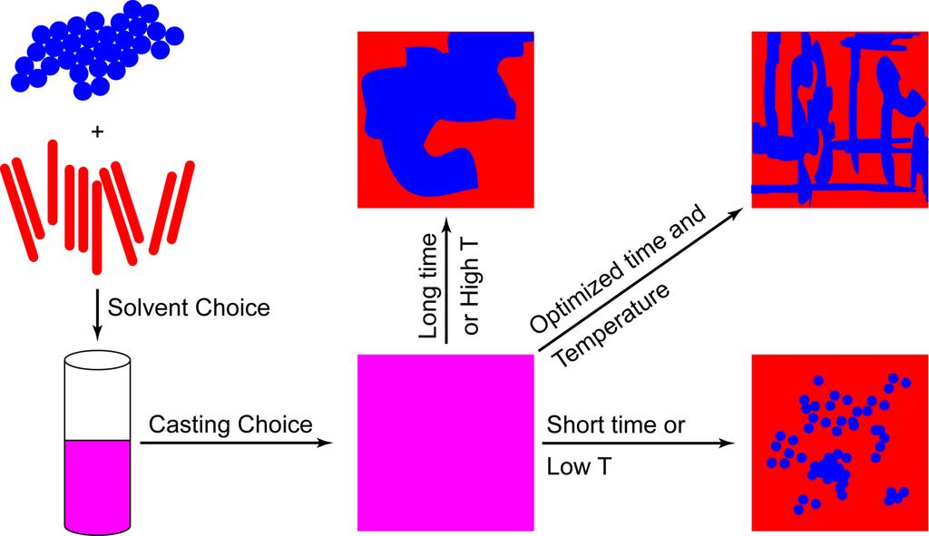
17 Current Active Layer Microstructures are History Dependent

18 Multiple Junction Solar Cells Extend Efficiencies to 11% Triple Junction Device Structure Triple Junction Device J-V Curves Further Reading: Chen, C.-C.; et al. Adv. Mater. 2014, 26, 5670.

19 An OLED Has a Similar Device Structure to an OPV General OLED Structure J-V Response and Emission Curves In OPV Devices, Light Was Input to Generate a Voltage In OLED Devices, a Voltage Bias is Applied to Generate the Emission of Light Holes are Injected from the Anode Electrons are Injected from the Cathode Recombination and Photoemission Occurs in the Organic Active Layer Further Reading: Tang, C. W.; Van Slyke, S. A. Appl. Phys. Lett. 1987, 51, 913.
 and Thermopower (S) while MINIMIZING Thermal Conductivity")
20 Thermoelectric Materials Convert Heat to Electricity Thermoelectric Device Schematic Efficiency Increases with Increasing ZT Figure of Merit η max = T HOT ZT = T T HOT COLD σ 2 S κ T ZT is Related to Efficiency 1+ ZT 1 T 1+ ZT T COLD HOT Goal is to MAXIMIZE Electrical Conductivity (σ) and Thermopower (S) while MINIMIZING Thermal Conductivity (κ)
21 Organic Electronics Have a Bright Future Organic Light-emitting Device (OLED) Displays Thin and Lightweight Flexible Transparent Sony Samsung Organic Photovoltaic (OPV) Devices Polytron Large Area Production Portable Applications Conformal Coverage Konarka Konarka Konarka
Organic Electronic Devices
 Organic Electronic Devices Week 4: Organic Photovoltaic Devices Lecture 4.1: Overview of Organic Photovoltaic Devices Bryan W. Boudouris Chemical Engineering Purdue University 1 Lecture Overview and Learning
Organic Electronic Devices
 Organic Electronic Devices Week 2: Electronic Structure Lecture 2.1: Atomic and Molecular Orbitals Bryan W. Boudouris Chemical Engineering Purdue University 1 Lecture Overview and Learning Objectives Concepts
Photovoltaics. Lecture 7 Organic Thin Film Solar Cells Photonics - Spring 2017 dr inż. Aleksander Urbaniak
 Photovoltaics Lecture 7 Organic Thin Film Solar Cells Photonics - Spring 2017 dr inż. Aleksander Urbaniak Barcelona, Spain Perpignan train station, France source: pinterest Why organic solar cells? 1.
Design of Optoelectronically-active Polymers for Organic Photovoltaic Applications
 Design of Optoelectronically-active Polymers for Organic Photovoltaic Applications Bryan W. Boudouris School of Chemical Engineering Purdue University Spring 2013 Solar Research Series Purdue University
ESE 372 / Spring 2013 / Lecture 5 Metal Oxide Semiconductor Field Effect Transistor
 Metal Oxide Semiconductor Field Effect Transistor V G V G 1 Metal Oxide Semiconductor Field Effect Transistor We will need to understand how this current flows through Si What is electric current? 2 Back
Charge Extraction from Complex Morphologies in Bulk Heterojunctions. Michael L. Chabinyc Materials Department University of California, Santa Barbara
 Charge Extraction from Complex Morphologies in Bulk Heterojunctions Michael L. Chabinyc Materials Department University of California, Santa Barbara OPVs Vs. Inorganic Thin Film Solar Cells Alta Devices
Semiconductor Polymer
 Semiconductor Polymer Organic Semiconductor for Flexible Electronics Introduction: An organic semiconductor is an organic compound that possesses similar properties to inorganic semiconductors with hole
David J. Starling Penn State Hazleton PHYS 214
 Being virtually killed by a virtual laser in a virtual space is just as effective as the real thing, because you are as dead as you think you are. -Douglas Adams, Mostly Harmless David J. Starling Penn
EE 346: Semiconductor Devices
 EE 346: Semiconductor Devices Lecture - 6 02/06/2017 Tewodros A. Zewde 1 DENSTY OF STATES FUNCTON Since current is due to the flow of charge, an important step in the process is to determine the number
Organic solar cells. State of the art and outlooks. Gilles Horowitz LPICM, UMR7647 CNRS - Ecole Polytechnique
 Organic solar cells. State of the art and outlooks Gilles Horowitz LPICM, UMR7647 CNRS - Ecole Polytechnique Solar energy Solar energy on earth: 75,000 tep/year 6000 times the world consumption in 2007
Calculating Band Structure
 Calculating Band Structure Nearly free electron Assume plane wave solution for electrons Weak potential V(x) Brillouin zone edge Tight binding method Electrons in local atomic states (bound states) Interatomic
Chemistry Instrumental Analysis Lecture 8. Chem 4631
 Chemistry 4631 Instrumental Analysis Lecture 8 UV to IR Components of Optical Basic components of spectroscopic instruments: stable source of radiant energy transparent container to hold sample device
Electrons are shared in covalent bonds between atoms of Si. A bound electron has the lowest energy state.
 Photovoltaics Basic Steps the generation of light-generated carriers; the collection of the light-generated carriers to generate a current; the generation of a large voltage across the solar cell; and
Electron Energy, E E = 0. Free electron. 3s Band 2p Band Overlapping energy bands. 3p 3s 2p 2s. 2s Band. Electrons. 1s ATOM SOLID.
 Electron Energy, E Free electron Vacuum level 3p 3s 2p 2s 2s Band 3s Band 2p Band Overlapping energy bands Electrons E = 0 1s ATOM 1s SOLID In a metal the various energy bands overlap to give a single
Vikram Kuppa School of Energy, Environmental, Biological and Medical Engineering College of Engineering and Applied Science University of Cincinnati
 Vikram Kuppa School of Energy, Environmental, Biological and Medical Engineering College of Engineering and Applied Science University of Cincinnati vikram.kuppa@uc.edu Fei Yu Yan Jin Andrew Mulderig Greg
ESE370: Circuit-Level Modeling, Design, and Optimization for Digital Systems
 ESE370: Circuit-Level Modeling, Design, and Optimization for Digital Systems Lec 6: September 14, 2015 MOS Model You are Here: Transistor Edition! Previously: simple models (0 and 1 st order) " Comfortable
Ch. 2: Energy Bands And Charge Carriers In Semiconductors
 Ch. 2: Energy Bands And Charge Carriers In Semiconductors Discrete energy levels arise from balance of attraction force between electrons and nucleus and repulsion force between electrons each electron
Basic Semiconductor Physics
 6 Basic Semiconductor Physics 6.1 Introduction With this chapter we start with the discussion of some important concepts from semiconductor physics, which are required to understand the operation of solar
Lecture (02) Introduction to Electronics II, PN Junction and Diodes I
 Introduction to Electronics II, PN Junction and Diodes I") Lecture (02) Introduction to Electronics II, PN Junction and Diodes I By: Dr. Ahmed ElShafee ١ Agenda Current in semiconductors/conductors N type, P type semiconductors N Type Semiconductor P Type Semiconductor
Lecture (02) Introduction to Electronics II, PN Junction and Diodes I By: Dr. Ahmed ElShafee ١ Agenda Current in semiconductors/conductors N type, P type semiconductors N Type Semiconductor P Type Semiconductor
The photovoltaic effect occurs in semiconductors where there are distinct valence and
 How a Photovoltaic Cell Works The photovoltaic effect occurs in semiconductors where there are distinct valence and conduction bands. (There are energies at which electrons can not exist within the solid)
Sheng S. Li. Semiconductor Physical Electronics. Second Edition. With 230 Figures. 4) Springer
 Springer") Sheng S. Li Semiconductor Physical Electronics Second Edition With 230 Figures 4) Springer Contents Preface 1. Classification of Solids and Crystal Structure 1 1.1 Introduction 1 1.2 The Bravais Lattice
Sheng S. Li Semiconductor Physical Electronics Second Edition With 230 Figures 4) Springer Contents Preface 1. Classification of Solids and Crystal Structure 1 1.1 Introduction 1 1.2 The Bravais Lattice
Basic cell design. Si cell
 Basic cell design Si cell 1 Concepts needed to describe photovoltaic device 1. energy bands in semiconductors: from bonds to bands 2. free carriers: holes and electrons, doping 3. electron and hole current:
smal band gap Saturday, April 9, 2011
 small band gap upper (conduction) band empty small gap valence band filled 2s 2p 2s 2p hybrid (s+p)band 2p no gap 2s (depend on the crystallographic orientation) extrinsic semiconductor semi-metal electron
Electronic Structure and Geometry Relaxation at Excited State
 Electronic Structure and Geometry Relaxation at Excited State Speaker: Chun I Wang ( 王俊壹 ) 2016.07.14 Structure-Performance Relationship Processing schemes Solvent quality Thermal annealing Blend composition
Halbleiter Prof. Yong Lei Prof. Thomas Hannappel
 Halbleiter Prof. Yong Lei Prof. Thomas Hannappel yong.lei@tu-ilmenau.de thomas.hannappel@tu-ilmenau.de http://www.tu-ilmenau.de/nanostruk/ Organic Semiconductors & Organic Electronics Organic semiconductors
Lecture 20: Semiconductor Structures Kittel Ch 17, p , extra material in the class notes
 Lecture 20: Semiconductor Structures Kittel Ch 17, p 494-503, 507-511 + extra material in the class notes MOS Structure Layer Structure metal Oxide insulator Semiconductor Semiconductor Large-gap Semiconductor
EECS130 Integrated Circuit Devices
 EECS130 Integrated Circuit Devices Professor Ali Javey 8/30/2007 Semiconductor Fundamentals Lecture 2 Read: Chapters 1 and 2 Last Lecture: Energy Band Diagram Conduction band E c E g Band gap E v Valence
Lecture (02) PN Junctions and Diodes
 PN Junctions and Diodes") Lecture (02) PN Junctions and Diodes By: Dr. Ahmed ElShafee ١ I Agenda N type, P type semiconductors N Type Semiconductor P Type Semiconductor PN junction Energy Diagrams of the PN Junction and Depletion
Lecture (02) PN Junctions and Diodes By: Dr. Ahmed ElShafee ١ I Agenda N type, P type semiconductors N Type Semiconductor P Type Semiconductor PN junction Energy Diagrams of the PN Junction and Depletion
Towards a deeper understanding of polymer solar cells
 Towards a deeper understanding of polymer solar cells Jan Anton Koster Valentin Mihailetchi Prof. Paul Blom Molecular Electronics Zernike Institute for Advanced Materials and DPI University of Groningen
Free Electron Model for Metals
 Free Electron Model for Metals Metals are very good at conducting both heat and electricity. A lattice of in a sea of electrons shared between all nuclei (moving freely between them): This is referred
Luminescence. Photoluminescence (PL) is luminescence that results from optically exciting a sample.
 is luminescence that results from optically exciting a sample.") Luminescence Topics Radiative transitions between electronic states Absorption and Light emission (spontaneous, stimulated) Excitons (singlets and triplets) Franck-Condon shift(stokes shift) and vibrational
Luminescence Topics Radiative transitions between electronic states Absorption and Light emission (spontaneous, stimulated) Excitons (singlets and triplets) Franck-Condon shift(stokes shift) and vibrational
Flexible Organic Photovoltaics Employ laser produced metal nanoparticles into the absorption layer 1. An Introduction
 Flexible Organic Photovoltaics Employ laser produced metal nanoparticles into the absorption layer 1. An Introduction Among the renewable energy sources that are called to satisfy the continuously increased
Lecture 7: Extrinsic semiconductors - Fermi level
 Lecture 7: Extrinsic semiconductors - Fermi level Contents 1 Dopant materials 1 2 E F in extrinsic semiconductors 5 3 Temperature dependence of carrier concentration 6 3.1 Low temperature regime (T < T
First-Hand Investigation: Modeling of Semiconductors
 perform an investigation to model the behaviour of semiconductors, including the creation of a hole or positive charge on the atom that has lost the electron and the movement of electrons and holes in
! Previously: simple models (0 and 1 st order) " Comfortable with basic functions and circuits. ! This week and next (4 lectures)
 Comfortable with basic functions and circuits. ! This week and next (4 lectures)") ESE370: CircuitLevel Modeling, Design, and Optimization for Digital Systems Lec 6: September 14, 2015 MOS Model You are Here: Transistor Edition! Previously: simple models (0 and 1 st order) " Comfortable
ESE370: CircuitLevel Modeling, Design, and Optimization for Digital Systems Lec 6: September 14, 2015 MOS Model You are Here: Transistor Edition! Previously: simple models (0 and 1 st order) " Comfortable
ELEMENTARY BAND THEORY
 ELEMENTARY BAND THEORY PHYSICIST Solid state band Valence band, VB Conduction band, CB Fermi energy, E F Bloch orbital, delocalized n-doping p-doping Band gap, E g Direct band gap Indirect band gap Phonon
Mesoporous titanium dioxide electrolyte bulk heterojunction
 Mesoporous titanium dioxide electrolyte bulk heterojunction The term "bulk heterojunction" is used to describe a heterojunction composed of two different materials acting as electron- and a hole- transporters,
Semiconductor Physics. Lecture 3
 Semiconductor Physics Lecture 3 Intrinsic carrier density Intrinsic carrier density Law of mass action Valid also if we add an impurity which either donates extra electrons or holes the number of carriers
Lecture 1. OUTLINE Basic Semiconductor Physics. Reading: Chapter 2.1. Semiconductors Intrinsic (undoped) silicon Doping Carrier concentrations
 silicon Doping Carrier concentrations") Lecture 1 OUTLINE Basic Semiconductor Physics Semiconductors Intrinsic (undoped) silicon Doping Carrier concentrations Reading: Chapter 2.1 EE105 Fall 2007 Lecture 1, Slide 1 What is a Semiconductor? Low
Lecture 1 OUTLINE Basic Semiconductor Physics Semiconductors Intrinsic (undoped) silicon Doping Carrier concentrations Reading: Chapter 2.1 EE105 Fall 2007 Lecture 1, Slide 1 What is a Semiconductor? Low
ESE370: Circuit-Level Modeling, Design, and Optimization for Digital Systems
 ESE370: Circuit-Level Modeling, Design, and Optimization for Digital Systems Lec 6: September 18, 2017 MOS Model You are Here: Transistor Edition! Previously: simple models (0 and 1 st order) " Comfortable
Planar Organic Photovoltaic Device. Saiful I. Khondaker
 Planar Organic Photovoltaic Device Saiful I. Khondaker Nanoscience Technology Center and Department of Physics University of Central Florida http://www.physics.ucf.edu/~khondaker W Metal 1 L ch Metal 2
ET3034TUx Utilization of band gap energy
 ET3034TUx - 3.3.1 - Utilization of band gap energy In the last two weeks we have discussed the working principle of a solar cell and the external parameters that define the performance of a solar cell.
MTLE-6120: Advanced Electronic Properties of Materials. Intrinsic and extrinsic semiconductors. Reading: Kasap:
 MTLE-6120: Advanced Electronic Properties of Materials 1 Intrinsic and extrinsic semiconductors Reading: Kasap: 5.1-5.6 Band structure and conduction 2 Metals: partially filled band(s) i.e. bands cross
e - Galvanic Cell 1. Voltage Sources 1.1 Polymer Electrolyte Membrane (PEM) Fuel Cell
 Fuel Cell") Galvanic cells convert different forms of energy (chemical fuel, sunlight, mechanical pressure, etc.) into electrical energy and heat. In this lecture, we are interested in some examples of galvanic cells.
Galvanic cells convert different forms of energy (chemical fuel, sunlight, mechanical pressure, etc.) into electrical energy and heat. In this lecture, we are interested in some examples of galvanic cells.
Nature of Lesson (Lecture/Tutorial) H3 WK No. Day/ Date. Remarks. Duration. 4.00pm 6.30pm ALL. 2.5 hours. Introduction to Semiconductors Lecture 01
 H3 WK No. Day/ Date. Remarks. Duration. 4.00pm 6.30pm ALL. 2.5 hours. Introduction to Semiconductors Lecture 01") JANUARY 2018 INTAKE Subject : Semiconductor Physics & Devices Venue : HCI Schedule : Mondays for Tutorial (3pm 5pm / 5pm 7pm) or Tuesdays for Tutorial (3pm 5pm / 5pm 7pm) and Thursdays for Lecture (4pm-6.30
JANUARY 2018 INTAKE Subject : Semiconductor Physics & Devices Venue : HCI Schedule : Mondays for Tutorial (3pm 5pm / 5pm 7pm) or Tuesdays for Tutorial (3pm 5pm / 5pm 7pm) and Thursdays for Lecture (4pm-6.30
Classification of Solids
 Classification of Solids Classification by conductivity, which is related to the band structure: (Filled bands are shown dark; D(E) = Density of states) Class Electron Density Density of States D(E) Examples
ECE 442. Spring, Lecture -2
 ECE 442 Power Semiconductor Devices and Integrated circuits Spring, 2006 University of Illinois at Chicago Lecture -2 Semiconductor physics band structures and charge carriers 1. What are the types of
What will it take for organic solar cells to be competitive?
 What will it take for organic solar cells to be competitive? Michael D. McGehee Stanford University Director of the Center for Advanced Molecular Photovoltaics Efficiency (%) We will need 20-25 % efficiency
ELEC 4700 Assignment #2
 ELEC 4700 Assignment #2 Question 1 (Kasop 4.2) Molecular Orbitals and Atomic Orbitals Consider a linear chain of four identical atoms representing a hypothetical molecule. Suppose that each atomic wavefunction
Nanotechnology and Solar Energy. Solar Electricity Photovoltaics. Fuel from the Sun Photosynthesis Biofuels Split Water Fuel Cells
 Nanotechnology and Solar Energy Solar Electricity Photovoltaics Fuel from the Sun Photosynthesis Biofuels Split Water Fuel Cells Solar cell A photon from the Sun generates an electron-hole pair in a semiconductor.
Semiconductor Devices and Circuits Fall Midterm Exam. Instructor: Dr. Dietmar Knipp, Professor of Electrical Engineering. Name: Mat. -Nr.
 Semiconductor Devices and Circuits Fall 2003 Midterm Exam Instructor: Dr. Dietmar Knipp, Professor of Electrical Engineering Name: Mat. -Nr.: Guidelines: Duration of the Midterm: 1 hour The exam is a closed
Free Electron Model for Metals
 Free Electron Model for Metals Metals are very good at conducting both heat and electricity. A lattice of in a sea of electrons shared between all nuclei (moving freely between them): This is referred
Lecture 18: Semiconductors - continued (Kittel Ch. 8)
") Lecture 18: Semiconductors - continued (Kittel Ch. 8) + a - Donors and acceptors J U,e e J q,e Transport of charge and energy h E J q,e J U,h Physics 460 F 2006 Lect 18 1 Outline More on concentrations
Lecture 18: Semiconductors - continued (Kittel Ch. 8) + a - Donors and acceptors J U,e e J q,e Transport of charge and energy h E J q,e J U,h Physics 460 F 2006 Lect 18 1 Outline More on concentrations
2.626 Fundamentals of Photovoltaics
 MIT OpenCourseWare http://ocw.mit.edu 2.626 Fundamentals of Photovoltaics Fall 2008 For information about citing these materials or our Terms of Use, visit: http://ocw.mit.edu/terms. Charge Separation:
A. OTHER JUNCTIONS B. SEMICONDUCTOR HETEROJUNCTIONS -- MOLECULES AT INTERFACES: ORGANIC PHOTOVOLTAIC BULK HETEROJUNCTION DYE-SENSITIZED SOLAR CELL
 A. OTHER JUNCTIONS B. SEMICONDUCTOR HETEROJUNCTIONS -- MOLECULES AT INTERFACES: ORGANIC PHOTOVOLTAIC BULK HETEROJUNCTION DYE-SENSITIZED SOLAR CELL February 9 and 14, 2012 The University of Toledo, Department
Introduction. Fang-Chung Chen Department of Photonics and Display Institute National Chiao Tung University. Organic light-emitting diodes
 rganic light-emitting diodes Introduction Fang-Chung Chen Department of Photonics and Display Institute National Chiao Tung University rganic light-emitting diodes --The emerging technology LED Displays
EECS143 Microfabrication Technology
 EECS143 Microfabrication Technology Professor Ali Javey Introduction to Materials Lecture 1 Evolution of Devices Yesterday s Transistor (1947) Today s Transistor (2006) Why Semiconductors? Conductors e.g
PHYS485 Materials Physics
 5/11/017 PHYS485 Materials Physics Dr. Gregory W. Clar Manchester University LET S GO ON A (TEK)ADVENTURE! WHAT? TRIP TO A MAKER S SPACE IN FORT WAYNE WHEN? THURSDAY, MAY 11 TH @ 5PM WHERE? TEKVENTURE
Semiconductor Physics and Devices Chapter 3.
 Introduction to the Quantum Theory of Solids We applied quantum mechanics and Schrödinger s equation to determine the behavior of electrons in a potential. Important findings Semiconductor Physics and
Electrons, Holes, and Defect ionization
 Electrons, Holes, and Defect ionization The process of forming intrinsic electron-hole pairs is excitation a cross the band gap ( formation energy ). intrinsic electronic reaction : null e + h When electrons
Variation of Energy Bands with Alloy Composition E
 Variation of Energy Bands with Alloy Composition E 3.0 E.8.6 L 0.3eV Al x GaAs AlAs 1- xas 1.43eV.16eV X k.4 L. X.0 X 1.8 L 1.6 1.4 0 0. 0.4 0.6 X 0.8 1 1 Carriers in intrinsic Semiconductors Ec 4º 1º
Semiconductor Physical Electronics
 Semiconductor Physical Electronics Sheng S. Li Department of Electrical Engineering University of Florida Gainesville, Florida Plenum Press New York and London Contents CHAPTER 1. Classification of Solids
Conductivity and Semi-Conductors
 Conductivity and Semi-Conductors J = current density = I/A E = Electric field intensity = V/l where l is the distance between two points Metals: Semiconductors: Many Polymers and Glasses 1 Electrical Conduction
3. Two-dimensional systems
 3. Two-dimensional systems Image from IBM-Almaden 1 Introduction Type I: natural layered structures, e.g., graphite (with C nanostructures) Type II: artificial structures, heterojunctions Great technological
Processing of Semiconducting Materials Prof. Pallab Banerji Department of Material Science Indian Institute of Technology, Kharagpur
 Processing of Semiconducting Materials Prof. Pallab Banerji Department of Material Science Indian Institute of Technology, Kharagpur Lecture - 4 Doping in Semiconductors Good morning. Let us start with
Review of Optical Properties of Materials
 Review of Optical Properties of Materials Review of optics Absorption in semiconductors: qualitative discussion Derivation of Optical Absorption Coefficient in Direct Semiconductors Photons When dealing
ECE 606 Homework Week 7 Mark Lundstrom Purdue University (revised 2/25/13) e E i! E T
 e E i! E T") ECE 606 Homework Week 7 Mark Lundstrom Purdue University (revised 2/25/13) 1) Consider an n- type semiconductor for which the only states in the bandgap are donor levels (i.e. ( E T = E D ). Begin with
ECE 606 Homework Week 7 Mark Lundstrom Purdue University (revised 2/25/13) 1) Consider an n- type semiconductor for which the only states in the bandgap are donor levels (i.e. ( E T = E D ). Begin with
n N D n p = n i p N A
 Summary of electron and hole concentration in semiconductors Intrinsic semiconductor: E G n kt i = pi = N e 2 0 Donor-doped semiconductor: n N D where N D is the concentration of donor impurity Acceptor-doped
Numerical model of planar heterojunction organic solar cells
 Article Materials Science July 2011 Vol.56 No.19: 2050 2054 doi: 10.1007/s11434-011-4376-4 SPECIAL TOPICS: Numerical model of planar heterojunction organic solar cells MA ChaoZhu 1 PENG YingQuan 12* WANG
ESE370: Circuit-Level Modeling, Design, and Optimization for Digital Systems. Today MOS MOS. Capacitor. Idea
 ESE370: Circuit-Level Modeling, Design, and Optimization for Digital Systems Day 9: September 26, 2011 MOS Model Today MOS Structure Basic Idea Semiconductor Physics Metals, insulators Silicon lattice
EE143 Fall 2016 Microfabrication Technologies. Evolution of Devices
 EE143 Fall 2016 Microfabrication Technologies Prof. Ming C. Wu wu@eecs.berkeley.edu 511 Sutardja Dai Hall (SDH) 1-1 Evolution of Devices Yesterday s Transistor (1947) Today s Transistor (2006) 1-2 1 Why
CLASS 12th. Semiconductors
 CLASS 12th Semiconductors 01. Distinction Between Metals, Insulators and Semi-Conductors Metals are good conductors of electricity, insulators do not conduct electricity, while the semiconductors have
Sébastien FORGET. Laboratoire de Physique des Lasers Université Paris Nord P13. www-lpl.univ-paris13.fr:8088/lumen/
 OLEDs Basic principles, technology and applications Sébastien FORGET Laboratoire de Physique des Lasers Université Paris Nord P13 www-lpl.univ-paris13.fr:8088/lumen/ Paris Nord University (Paris 13) This
4.2 Molecular orbitals and atomic orbitals Consider a linear chain of four identical atoms representing a hypothetical molecule.
 4. Molecular orbitals and atomic orbitals Consider a linear chain of four identical atoms representing a hypothetical molecule. Suppose that each atomic wavefunction is 1s wavefunction. This system of
Novel Soft Materials: Organic Semiconductors
 JSPS Science Dialogue Novel Soft Materials: Organic Semiconductors X.T. HAO Prof. UENO s Lab Faculty of Engineering, Chiba University 21 st Century Center of Excellence Program The route to research Transparent
! Previously: simple models (0 and 1 st order) " Comfortable with basic functions and circuits. ! This week and next (4 lectures)
 Comfortable with basic functions and circuits. ! This week and next (4 lectures)") ESE370: CircuitLevel Modeling, Design, and Optimization for Digital Systems Lec 6: September 18, 2017 MOS Model You are Here: Transistor Edition! Previously: simple models (0 and 1 st order) " Comfortable
ESE370: CircuitLevel Modeling, Design, and Optimization for Digital Systems Lec 6: September 18, 2017 MOS Model You are Here: Transistor Edition! Previously: simple models (0 and 1 st order) " Comfortable
Surface Transfer Doping of Diamond by Organic Molecules
 Surface Transfer Doping of Diamond by Organic Molecules Qi Dongchen Department of Physics National University of Singapore Supervisor: Prof. Andrew T. S. Wee Dr. Gao Xingyu Scope of presentation Overview
Diodes. anode. cathode. cut-off. Can be approximated by a piecewise-linear-like characteristic. Lecture 9-1
 Diodes mplest nonlinear circuit element Basic operation sets the foundation for Bipolar Junction Transistors (BJTs) Also present in Field Effect Transistors (FETs) Ideal diode characteristic anode cathode
FREQUENTLY ASKED QUESTIONS February 21, 2017
 FREQUENTLY ASKED QUESTIONS February 21, 2017 Content Questions How do you place a single arsenic atom with the ratio 1 in 100 million? Sounds difficult to get evenly spread throughout. Yes, techniques
Semiconductor device structures are traditionally divided into homojunction devices
 0. Introduction: Semiconductor device structures are traditionally divided into homojunction devices (devices consisting of only one type of semiconductor material) and heterojunction devices (consisting
Senior Project Thesis Senior Project Committee, Department of Physics, Case Western Reserve University
 Liquid Crystal Semiconductor Nanostructures Richard Metzger,Department of Physics, Case Western Reserve University Nick Lind, Department of Physics, Case Western Reserve University Professor K. Singer,
Plastic Electronics. Joaquim Puigdollers.
 Plastic Electronics Joaquim Puigdollers Joaquim.puigdollers@upc.edu Nobel Prize Chemistry 2000 Origins Technological Interest First products.. MONOCROMATIC PHILIPS Today Future Technological interest Low
3.1 Introduction to Semiconductors. Y. Baghzouz ECE Department UNLV
 3.1 Introduction to Semiconductors Y. Baghzouz ECE Department UNLV Introduction In this lecture, we will cover the basic aspects of semiconductor materials, and the physical mechanisms which are at the
Chapter 12: Semiconductors
 Chapter 12: Semiconductors Bardeen & Shottky January 30, 2017 Contents 1 Band Structure 4 2 Charge Carrier Density in Intrinsic Semiconductors. 6 3 Doping of Semiconductors 12 4 Carrier Densities in Doped
The Semiconductor in Equilibrium
 Lecture 6 Semiconductor physics IV The Semiconductor in Equilibrium Equilibrium, or thermal equilibrium No external forces such as voltages, electric fields. Magnetic fields, or temperature gradients are
From Last Time Important new Quantum Mechanical Concepts. Atoms and Molecules. Today. Symmetry. Simple molecules.
 Today From Last Time Important new Quantum Mechanical Concepts Indistinguishability: Symmetries of the wavefunction: Symmetric and Antisymmetric Pauli exclusion principle: only one fermion per state Spin
Lecture 20 - Semiconductor Structures
 Lecture 0: Structures Kittel Ch 17, p 494-503, 507-511 + extra material in the class notes MOS Structure metal Layer Structure Physics 460 F 006 Lect 0 1 Outline What is a semiconductor Structure? Created
Lecture 3b. Bonding Model and Dopants. Reading: (Cont d) Notes and Anderson 2 sections
 Notes and Anderson 2 sections") Lecture 3b Bonding Model and Dopants Reading: (Cont d) Notes and Anderson 2 sections 2.3-2.7 The need for more control over carrier concentration Without help the total number of carriers (electrons and
Lecture 3b Bonding Model and Dopants Reading: (Cont d) Notes and Anderson 2 sections 2.3-2.7 The need for more control over carrier concentration Without help the total number of carriers (electrons and
2. The electrochemical potential and Schottky barrier height should be quantified in the schematic of Figure 1.
 Reviewers' comments: Reviewer #1 (Remarks to the Author): The paper reports a photon enhanced thermionic effect (termed the photo thermionic effect) in graphene WSe2 graphene heterostructures. The work
PHYS208 p-n junction. January 15, 2010
 1 PHYS208 p-n junction January 15, 2010 List of topics (1) Density of states Fermi-Dirac distribution Law of mass action Doped semiconductors Dopinglevel p-n-junctions 1 Intrinsic semiconductors List of
Conjugated Polymers Based on Benzodithiophene for Organic Solar Cells. Wei You
 Wake Forest Nanotechnology Conference October 19, 2009 Conjugated Polymers Based on Benzodithiophene for Organic olar Cells Wei You Department of Chemistry and Institute for Advanced Materials, Nanoscience
1 Name: Student number: DEPARTMENT OF PHYSICS AND PHYSICAL OCEANOGRAPHY MEMORIAL UNIVERSITY OF NEWFOUNDLAND. Fall :00-11:00
 1 Name: DEPARTMENT OF PHYSICS AND PHYSICAL OCEANOGRAPHY MEMORIAL UNIVERSITY OF NEWFOUNDLAND Final Exam Physics 3000 December 11, 2012 Fall 2012 9:00-11:00 INSTRUCTIONS: 1. Answer all seven (7) questions.
CME 300 Properties of Materials. ANSWERS: Homework 9 November 26, As atoms approach each other in the solid state the quantized energy states:
 CME 300 Properties of Materials ANSWERS: Homework 9 November 26, 2011 As atoms approach each other in the solid state the quantized energy states: are split. This splitting is associated with the wave
Semiconductors. SEM and EDAX images of an integrated circuit. SEM EDAX: Si EDAX: Al. Institut für Werkstoffe der ElektrotechnikIWE
 SEM and EDAX images of an integrated circuit SEM EDAX: Si EDAX: Al source: [Cal 99 / 605] M&D-.PPT, slide: 1, 12.02.02 Classification semiconductors electronic semiconductors mixed conductors ionic conductors
Introduction to Organic Solar Cells
 Introduction to Organic Solar Cells Dr Chris Fell Solar Group Leader CSIRO Energy Technology, Newcastle, Australia Organic semiconductors Conductivity in polyacetylene 1970s Nobel Prize Alan J. Heeger
LECTURE 23. MOS transistor. 1 We need a smart switch, i.e., an electronically controlled switch. Lecture Digital Circuits, Logic
 LECTURE 23 Lecture 16-20 Digital Circuits, Logic 1 We need a smart switch, i.e., an electronically controlled switch 2 We need a gain element for example, to make comparators. The device of our dreams
Basic Limitations to Third generation PV performance
 Basic Limitations to Third generation PV performance Pabitra K. Nayak Weizmann Institute of Science, Rehovot, Israel THANKS to my COLLEAGUES Lee Barnea and David Cahen. Weizmann Institute of Science Juan
Crystal Properties. MS415 Lec. 2. High performance, high current. ZnO. GaN
 Crystal Properties Crystal Lattices: Periodic arrangement of atoms Repeated unit cells (solid-state) Stuffing atoms into unit cells Determine mechanical & electrical properties High performance, high current
Atoms? All matters on earth made of atoms (made up of elements or combination of elements).
.") Chapter 1 Atoms? All matters on earth made of atoms (made up of elements or combination of elements). Atomic Structure Atom is the smallest particle of an element that can exist in a stable or independent
Chapter 1 Atoms? All matters on earth made of atoms (made up of elements or combination of elements). Atomic Structure Atom is the smallest particle of an element that can exist in a stable or independent
Engineering 2000 Chapter 8 Semiconductors. ENG2000: R.I. Hornsey Semi: 1
 Engineering 2000 Chapter 8 Semiconductors ENG2000: R.I. Hornsey Semi: 1 Overview We need to know the electrical properties of Si To do this, we must also draw on some of the physical properties and we