Review of Optical Properties of Materials
|
|
|
- Leo Rogers
- 5 years ago
- Views:
Transcription
1 Review of Optical Properties of Materials Review of optics Absorption in semiconductors: qualitative discussion Derivation of Optical Absorption Coefficient in Direct Semiconductors
2 Photons When dealing with events on the atomic scale, it is often best to regard light as composed of quasi- particles PHOTONS Photons are Quanta of light Electromagnetic radiation is quantized & occurs in finite "bundles" of energy Photons The energy of a single photon in terms of its frequency, or wavelength is, E ph = h = (hc)/
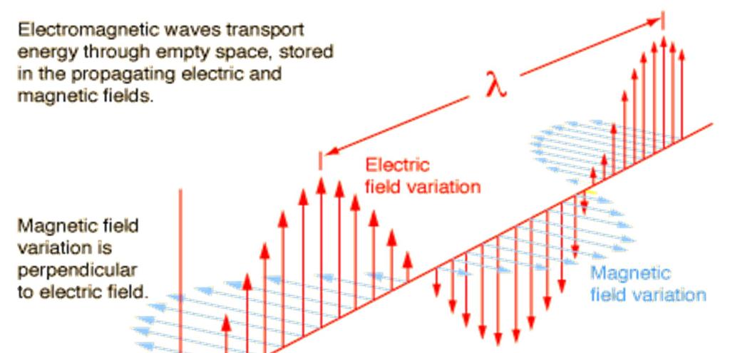
3 Maxwell Electromagnetic Waves
4 Light as an Electromagnetic Wave Light as an electromagnetic wave is characterized by a combination of a time-varying electric field (E) & magnetic field (H) propagating through space. Maxwell s equations give the result that both E & H satisfy the same wave equation: 1 c t EH, EH, Changes in the fields propagate through space with speed c.

5 Speed of Light, c Frequency of oscillation, of the fields and their wavelength, o in vacuum are related by; c = o In any other medium the speed, v is given by; v= c/n = n = refractive index of the medium = wavelength in the medium And, n r r r = relative magnetic permeability of the medium r = relative electric permittivity of the medium The speed of light in a medium is related to the electric and magnetic properties of the medium, and the speed of light can be expressed as
6 Electromagnetic Spectrum Shorter wavelength Larger Photon Energy (ev) Longer wavelength
7 Interaction Between Light & Bulk Material Many different possible processes can occur! Incident light 3a 3c Semi-transparent material 1 4 3b Scattering 1- Refraction - Transmission 3a Specular reflection 3b Total internal reflection 3c Diffused reflection 4 Dispersion where different colors bend differently


8 Refraction, Reflection and Dispersion Light when it travels in a medium can be absorbed and reemitted by every atom in its path. Small n Determined by refractive index; n High n n 1 = refractive index of material 1 n = refractive index of material
9 Total Internal Reflection Transmitted (refracted) light t k t n Evanescent wave k i Incident light i i k r n > n 1 c c i > c TIR Reflected light (a) (b) (c) Light wave travelling in a more dense medium strikes a less dense medium. Depending on the incidence angle with respect to c, which is determined by the ratio of the refractive indices, the wave may be transmitted (refracted) or reflected. (a) i < c (b) i = c (c) i > c and total internal reflection (TIR) S.O. Kasap, Optoelectronics (Prentice Hall)


10 Mechanism and Application of TIR Optical fibre for communication What sort of materials do you think are suitable for fibre optics cables?

11 Review of optical processes Energy levels are everything in quantum mechanics. Excited level Energy E = h Ground level The atom is vibrating at frequency,. The atom is at least partially in an excited state.
12 Review of optical processes Before After Spontaneous emission Absorption Stimulated emission
13 Recall: Semiconductor Bandgaps E g are usually in the range: 0 < E g < 3 ev (up to 6 ev if diamond is included) Also, at equilibrium, at temperature T = 0, the valence band is full & the conduction band is empty. Now, consider what happens if electromagnetic radiation ( light ) is shined on the material. In the photon representation of this radiation If hν E g, some electrons can be promoted to the conduction band leaving some holes in the valence band.
14 Consider various types of spectra associated with this process: Absorption: Looks at the number of absorbed photons (intensity) vs. photon frequency ω Reflection: Looks at the number of reflected photons (intensity) vs. photon frequency ω Transmission: Looks at the number of transmitted photons (intensity) vs. photon frequency ω Emission: Looks at the number of emitted photons (intensity) vs. photon frequency ω Each of these types of spectra are Understanding such spectra gives rich, complicated, & varied! huge amounts of information about electronic energy bands, vibrational properties, defects,
15 Appearance of insulator, metal and semiconductor Appearance in terms of color depends on the interaction between the light with the electronics configuration of the material. Normally, High resistivity material: insulator transparent High conductivity material: metals metallic luster and opaque Semiconductors colored, opaque or transparent, color depending on the band gap of the material For semiconductors the energy band diagram can explain the appearance of the material in terms of luster and color.

16 Question: Why is Silicon Black and Shiny?
17 Answer. Need to know, the energy gap of Si E gap = 1.eV Need to know visible light photon energy E vis ~ eV E vis is larger than Silicon E gap All visible light will be absorbed Silicon appears black Why is Si shiny? Significant photon absorption occurs in silicon, because there are a significant number of electrons in the conduction band. These electrons are delocalized. They scatter photons.
18 Colors of Semiconductors E vis = 1.8eV 3.1eV I B G Y O R If Photon Energy, E vis > E gap Photons will be absorbed If Photon Energy, E vis < E gap Photons will be transmitted If Photon Energy is in the range of E gap ; Those with higher energy than E gap will be absorbed. We see the color of the light being transmitted If all colors are transmitted = White
19 Why is glass transparent? Glass is an insulator (huge band gap) The electrons find it hard to jump across a big energy gap: E gap >> 5eV E gap >> E visible spectrum ~ eV All colored photons are transmitted, no absorption, hence light transmission transparent. Defined transmission and absorption by Lambert s law: I = I o exp (- l) I = incident beam I o = transmitted beam = total linear absorption coefficient (m -1 ) = takes into account the loss of intensity from both scattering centers and absorption centers. = approaching zero for pure insulator.
20 What happens during photon absorption process? Photon interacts with the lattice Photon interacts with defects Photon interacts with valance electrons
21 Absorption an important phenomenon in describing optical properties of semiconductors Light, being a form of electromagnetic radiation, interacts with the electronic structure of atoms of a material. The initial interaction is one of absorption; that is, the electrons of atoms on the surface of a material will absorb the energy of the colliding photons of light and move to the higher-energy states. The degree of absorption depends, among other things, on the number of free electrons capable of receiving this photon energy.
22 Absorption Process of Semiconductors The interaction process is a characteristic of a photon and depends on the energy of the photon Low-energy photons interact principally by ionization or excitation of the outer orbitals in solids atoms. Light of low-energy photons (< 10 ev) is represented by infrared (IR), visible light, and ultraviolet (UV) in the electromagnetic spectrum. High-energy protons (> 10 4 ev) such as x-rays (and gamma rays) scatter mainly elastically and are used for structure determination The minimum photon energy required to excite and/or ionize the component atoms of a solid is called the absorption edge or threshold.
23 Absorption Process of Semiconductors Absorption coefficient (), cm -1 UV Important region: Wavelength (m) E g ~ vis Vis IR Photon energy (ev) Absorption spectrum of a semiconductor.
24 Valance-Conduction Absorption Process requires the lowest E of photon to initiate electron jumping (excitation) E C -E V = h Conduction band, E C E C -E V = E gap If h > E gap then transition happens E gap h E photon Electrons in the conduction band and excited. Valance band, E V
25 Absorption Types Direct and Indirect photon absorption For all absorption process there must be: Conservation of energy Conservation of momentum or the wavevector The production of e-h pairs is very important for various electronics devices especially the photovoltaic and photodetectors devices. The absorbed light can be transformed to current in these devices
26 Direct Band Gap E Direct vertical transition Conservation of E h = E C(min) -E v (max) = E gap Momentum of photon is negligible K (wave number) Conservation of wavevector K vmax + photon = kc h
27 Interband absorption in indirect gap semiconductors Indirect-gap semiconductor: highest occupied and lowest unoccupied state have k 0 Direct transitions possible for k0 strong direct interband absorption occurs at E > E gap E gap Other possibility: momentum and energy can be conserved by photon absorption and simultaneous absorption or emission of a phonon: Indirect transitions possible with assistance of a phonon Shown here are optically induced transitions E gap - during phonon emission a phonon is generated in the process - during phonon absorption a phonon is generated in the process
28 Excitons Excitons are combined electron-hole states: A free electron and a free hole (empty electronic state in the valence band) exert Coulomb force on each other: hydrogen-like bound states possible: excitonic states e n=3 n= n=1 Coulomb force h E b E E b is the exciton binding energy = energy released upon exciton formation, or k energy required for exciton breakup Wave functions of electron and hole look similar to free electron and free hole Note: exciton can move through crystal, i.e. not bound to specific atom!
29 Excitonic absorption Light can excite an electron from the valence band and generate an exciton at energies slightly below the bandgap see absorption at E phot = E gap E b (absorption slightly below E gap ) E E b k Exciton binding energy on the order of a few mev Thermal energy at room temperature: kt ~ 5 mev exciton rapidly dissociates at room temperature absorption lines broaden / disappear for higher temperatures


30 Optical transitions related to dopant atoms Ga: 3 valence electrons Si: 4 valence electrons As: 5 valence electrons
31 Donor levels Substitute Si atom with As atom (impurity atom in the Si lattice): weakly bound extra valence electron Low T Low T: donors neutral, electron weakly bound low energy light can excite donor electron in to conduciton band Binding energy E d similar to kt at room temperature ( RT ): At room temperature the bound electron is quickly released impurity mostly ionized at RT : Arsenic is a donor in Si RT At RT such transitions are typically too broad to observe
32 Acceptor levels Substitute Si atom with Ga atom : empty electronic state just above the Si valence band: at finite temperature, Si valence electron may fill acceptor level location of unoccupied valence state (hole) can orbit the charged Ga dopant hole = available electron state Binding energy E a similar to kt at room temperature ( RT ): At room temperature the hole can leave the dopant, producing a free charge
33 Infrared absorption due to dopants Dopant binding energies low: donor level related absorptions invisible at RT, but observable at low temperatures Example: direct valence band acceptor level absorption in boron doped Si Transition at ~40 mev absorption at 30 m : infrared
34 Dopant related transitions Possible dopant related transitions: Typically visible at low T, but not clearly observable at RT
35 Free carrier absorption At RT, predominant dopant related absorption is free carrier absorption in which a photon excites an electron into a higher lying state Example: p-type semiconductors: filled states in the conduction band: optical transitions possible at E phot < E gap! Free electrons: absorption typically indirect phonon-assisted transition Free holes can make direct transitions from the heavy-hole band to the light-hole band holes cause stronger free carrier absorption than electrons
36 Free carrier absorption Free electron absorption can be described by the Drude model Dopant levels in semiconductors range from ~ /cm 3 which is ~ lower than free electron densities in metals Plasma frequency of doped semiconductors lower than of metals: IR 3 3 ) "(, 1 ) '( p p r p r ) "( ) ( p p c c c At frequencies above plasma frequency, ε r is complex and is described by Electron FCA up for lower energies Free hole absorption less well defined
37 Derivation of Optical Absorption Coefficient in Direct Semiconductors Chuang Ch. 9

38 Outline of derivation Absorption Coefficient: ( ) I(, z) I (, z) e o ( ) z Examples: lasers, solar cells, etc. Time-dependent perturbation Fermi s Golden rule poly-si Solar Cells Direct-gap net absorption rate Absorption Coefficient & Simplifications
39 Fermi s Golden Rule ' W i f Hfi ( ( Ef Ei ) ( Ef Ei )) E f E i E i E f Absorption Emission
40 Direct-Gap Net Absorption Rate E c E π R H' δ(ε Ε )f 1f V vc cv c v v c k k k v c Assumptions: k v = k c = k Undoped, low excitation E v f v = 1, f c = 0 E E v c k * mh E g k m * e R abs π H ' cv δ(εc Ε v ) V k
41 ( ) How to find H cv? H ( r, t) H ' ( r ) Absorption Coefficient R abs P / nc A V ( r o o /) 1 m o ea m pˆ ea V ( r ) o o eˆ (no. of photons absorbed per second per unit volume) (no. of injected photons per second per unit area) pˆ r o o H ' cv k π H ' cv δ(ε c Ε v ) ψ * c H' ( r ) ψ πe ( ) eˆ pcv δ(εc Ε v ) nc m V k v d Momentum matrix element 3 r
42 ( ) More Practical Form πe V k nc m V m 3 eˆ p cv δ(e 3 g ) k r o o k r ep δ(e )d k nc m m ( ) πe eˆ pcv NJ ( Eg ) nc m m oeg 1 p cv 1 me r o o πe k 3 ˆ cv 3 g r o o r Using E-k (dispersion) relationship: ( ) nc 3/ πe 1 1/ ˆ mr e p cv k δ(e g k )d k r omo 3/ 1 mr NJ( k) k
43 Conclusions Absorption Coefficient at 5K Example: InSb Eg = 0.17eV Different for D,1D,0D Density of States Yu, Cardona: p. 60 Red: calculation at 300K Not 100% accurate Parabolic band approximation n r depends on wavelength Exciton absorption below bandgap
EECS130 Integrated Circuit Devices
 EECS130 Integrated Circuit Devices Professor Ali Javey 8/30/2007 Semiconductor Fundamentals Lecture 2 Read: Chapters 1 and 2 Last Lecture: Energy Band Diagram Conduction band E c E g Band gap E v Valence
Lecture 15: Optoelectronic devices: Introduction
 Lecture 15: Optoelectronic devices: Introduction Contents 1 Optical absorption 1 1.1 Absorption coefficient....................... 2 2 Optical recombination 5 3 Recombination and carrier lifetime 6 3.1
ELECTRONIC DEVICES AND CIRCUITS SUMMARY
 ELECTRONIC DEVICES AND CIRCUITS SUMMARY Classification of Materials: Insulator: An insulator is a material that offers a very low level (or negligible) of conductivity when voltage is applied. Eg: Paper,
EECS143 Microfabrication Technology
 EECS143 Microfabrication Technology Professor Ali Javey Introduction to Materials Lecture 1 Evolution of Devices Yesterday s Transistor (1947) Today s Transistor (2006) Why Semiconductors? Conductors e.g
Chapter 1 Overview of Semiconductor Materials and Physics
 Chapter 1 Overview of Semiconductor Materials and Physics Professor Paul K. Chu Conductivity / Resistivity of Insulators, Semiconductors, and Conductors Semiconductor Elements Period II III IV V VI 2 B
Session 5: Solid State Physics. Charge Mobility Drift Diffusion Recombination-Generation
 Session 5: Solid State Physics Charge Mobility Drift Diffusion Recombination-Generation 1 Outline A B C D E F G H I J 2 Mobile Charge Carriers in Semiconductors Three primary types of carrier action occur
Chemistry Instrumental Analysis Lecture 8. Chem 4631
 Chemistry 4631 Instrumental Analysis Lecture 8 UV to IR Components of Optical Basic components of spectroscopic instruments: stable source of radiant energy transparent container to hold sample device
Optical Properties of Solid from DFT
 Optical Properties of Solid from DFT 1 Prof.P. Ravindran, Department of Physics, Central University of Tamil Nadu, India & Center for Materials Science and Nanotechnology, University of Oslo, Norway http://folk.uio.no/ravi/cmt15
CME 300 Properties of Materials. ANSWERS: Homework 9 November 26, As atoms approach each other in the solid state the quantized energy states:
 CME 300 Properties of Materials ANSWERS: Homework 9 November 26, 2011 As atoms approach each other in the solid state the quantized energy states: are split. This splitting is associated with the wave
Minimal Update of Solid State Physics
 Minimal Update of Solid State Physics It is expected that participants are acquainted with basics of solid state physics. Therefore here we will refresh only those aspects, which are absolutely necessary
Luminescence Process
 Luminescence Process The absorption and the emission are related to each other and they are described by two terms which are complex conjugate of each other in the interaction Hamiltonian (H er ). In an
EE143 Fall 2016 Microfabrication Technologies. Evolution of Devices
 EE143 Fall 2016 Microfabrication Technologies Prof. Ming C. Wu wu@eecs.berkeley.edu 511 Sutardja Dai Hall (SDH) 1-1 Evolution of Devices Yesterday s Transistor (1947) Today s Transistor (2006) 1-2 1 Why
Direct and Indirect Semiconductor
 Direct and Indirect Semiconductor Allowed values of energy can be plotted vs. the propagation constant, k. Since the periodicity of most lattices is different in various direction, the E-k diagram must
The Semiconductor in Equilibrium
 Lecture 6 Semiconductor physics IV The Semiconductor in Equilibrium Equilibrium, or thermal equilibrium No external forces such as voltages, electric fields. Magnetic fields, or temperature gradients are
3.1 Introduction to Semiconductors. Y. Baghzouz ECE Department UNLV
 3.1 Introduction to Semiconductors Y. Baghzouz ECE Department UNLV Introduction In this lecture, we will cover the basic aspects of semiconductor materials, and the physical mechanisms which are at the
Luminescence basics. Slide # 1
 Luminescence basics Types of luminescence Cathodoluminescence: Luminescence due to recombination of EHPs created by energetic electrons. Example: CL mapping system Photoluminescence: Luminescence due to
PHYSICS nd TERM Outline Notes (continued)
") PHYSICS 2800 2 nd TERM Outline Notes (continued) Section 6. Optical Properties (see also textbook, chapter 15) This section will be concerned with how electromagnetic radiation (visible light, in particular)
PHYSICS 2800 2 nd TERM Outline Notes (continued) Section 6. Optical Properties (see also textbook, chapter 15) This section will be concerned with how electromagnetic radiation (visible light, in particular)
Electronic and Optoelectronic Properties of Semiconductor Structures
 Electronic and Optoelectronic Properties of Semiconductor Structures Jasprit Singh University of Michigan, Ann Arbor CAMBRIDGE UNIVERSITY PRESS CONTENTS PREFACE INTRODUCTION xiii xiv 1.1 SURVEY OF ADVANCES
Lecture 20 Optical Characterization 2
 Lecture 20 Optical Characterization 2 Schroder: Chapters 2, 7, 10 1/68 Announcements Homework 5/6: Is online now. Due Wednesday May 30th at 10:00am. I will return it the following Wednesday (6 th June).
Engineering 2000 Chapter 8 Semiconductors. ENG2000: R.I. Hornsey Semi: 1
 Engineering 2000 Chapter 8 Semiconductors ENG2000: R.I. Hornsey Semi: 1 Overview We need to know the electrical properties of Si To do this, we must also draw on some of the physical properties and we
Optical Properties of Lattice Vibrations
 Optical Properties of Lattice Vibrations For a collection of classical charged Simple Harmonic Oscillators, the dielectric function is given by: Where N i is the number of oscillators with frequency ω
Chapter 12: Semiconductors
 Chapter 12: Semiconductors Bardeen & Shottky January 30, 2017 Contents 1 Band Structure 4 2 Charge Carrier Density in Intrinsic Semiconductors. 6 3 Doping of Semiconductors 12 4 Carrier Densities in Doped
Chapter 2 Optical Transitions
 Chapter 2 Optical Transitions 2.1 Introduction Among energy states, the state with the lowest energy is most stable. Therefore, the electrons in semiconductors tend to stay in low energy states. If they
Bohr s Model, Energy Bands, Electrons and Holes
 Dual Character of Material Particles Experimental physics before 1900 demonstrated that most of the physical phenomena can be explained by Newton's equation of motion of material particles or bodies and
Optical Properties of Semiconductors. Prof.P. Ravindran, Department of Physics, Central University of Tamil Nadu, India
 Optical Properties of Semiconductors 1 Prof.P. Ravindran, Department of Physics, Central University of Tamil Nadu, India http://folk.uio.no/ravi/semi2013 Light Matter Interaction Response to external electric
Basic Principles of Light Emission in Semiconductors
 Basic Principles of Light Emission in Semiconductors Class: Integrated Photonic Devices Time: Fri. 8:00am ~ 11:00am. Classroom: 資電 06 Lecturer: Prof. 李明昌 (Ming-Chang Lee) Model for Light Generation and
Lecture 1. OUTLINE Basic Semiconductor Physics. Reading: Chapter 2.1. Semiconductors Intrinsic (undoped) silicon Doping Carrier concentrations
 silicon Doping Carrier concentrations") Lecture 1 OUTLINE Basic Semiconductor Physics Semiconductors Intrinsic (undoped) silicon Doping Carrier concentrations Reading: Chapter 2.1 EE105 Fall 2007 Lecture 1, Slide 1 What is a Semiconductor? Low
Lecture 1 OUTLINE Basic Semiconductor Physics Semiconductors Intrinsic (undoped) silicon Doping Carrier concentrations Reading: Chapter 2.1 EE105 Fall 2007 Lecture 1, Slide 1 What is a Semiconductor? Low
MTLE-6120: Advanced Electronic Properties of Materials. Intrinsic and extrinsic semiconductors. Reading: Kasap:
 MTLE-6120: Advanced Electronic Properties of Materials 1 Intrinsic and extrinsic semiconductors Reading: Kasap: 5.1-5.6 Band structure and conduction 2 Metals: partially filled band(s) i.e. bands cross
Mat E 272 Lecture 25: Electrical properties of materials
 Mat E 272 Lecture 25: Electrical properties of materials December 6, 2001 Introduction: Calcium and copper are both metals; Ca has a valence of +2 (2 electrons per atom) while Cu has a valence of +1 (1
From Last Time Important new Quantum Mechanical Concepts. Atoms and Molecules. Today. Symmetry. Simple molecules.
 Today From Last Time Important new Quantum Mechanical Concepts Indistinguishability: Symmetries of the wavefunction: Symmetric and Antisymmetric Pauli exclusion principle: only one fermion per state Spin
EE495/695 Introduction to Semiconductors I. Y. Baghzouz ECE Department UNLV
 EE495/695 Introduction to Semiconductors I Y. Baghzouz ECE Department UNLV Introduction Solar cells have always been aligned closely with other electronic devices. We will cover the basic aspects of semiconductor
Semiconductor Physics and Devices Chapter 3.
 Introduction to the Quantum Theory of Solids We applied quantum mechanics and Schrödinger s equation to determine the behavior of electrons in a potential. Important findings Semiconductor Physics and
SEMICONDUCTOR PHYSICS
 SEMICONDUCTOR PHYSICS by Dibyendu Chowdhury Semiconductors The materials whose electrical conductivity lies between those of conductors and insulators, are known as semiconductors. Silicon Germanium Cadmium
Lecture 3: Optical Properties of Insulators, Semiconductors, and Metals. 5 nm
 Metals Lecture 3: Optical Properties of Insulators, Semiconductors, and Metals 5 nm Course Info Next Week (Sept. 5 and 7) no classes First H/W is due Sept. 1 The Previous Lecture Origin frequency dependence
I. Introduction II. Solid State Physics Detection of Light Bernhard Brandl 1
 Detection of Light I. Introduction II. Solid State Physics 4-2-2015 Detection of Light Bernhard Brandl 1 4-2-2015 Detection of Light Bernhard Brandl 2 Blabla Recommended 4-2-2015 Detection of Light Bernhard
Modern Physics for Frommies IV The Universe - Small to Large Lecture 4
 Fromm Institute for Lifelong Learning University of San Francisco Modern Physics for Frommies IV The Universe - Small to Large Lecture 4 3 February 06 Modern Physics IV Lecture 4 Agenda Administrative
Basic cell design. Si cell
 Basic cell design Si cell 1 Concepts needed to describe photovoltaic device 1. energy bands in semiconductors: from bonds to bands 2. free carriers: holes and electrons, doping 3. electron and hole current:
Chapter Two. Energy Bands and Effective Mass
 Chapter Two Energy Bands and Effective Mass Energy Bands Formation At Low Temperature At Room Temperature Valence Band Insulators Metals Effective Mass Energy-Momentum Diagrams Direct and Indirect Semiconduction
Free Electron Model for Metals
 Free Electron Model for Metals Metals are very good at conducting both heat and electricity. A lattice of in a sea of electrons shared between all nuclei (moving freely between them): This is referred
OPTICAL PROPERTIES of Nanomaterials
 OPTICAL PROPERTIES of Nanomaterials Advanced Reading Optical Properties and Spectroscopy of Nanomaterials Jin Zhong Zhang World Scientific, Singapore, 2009. Optical Properties Many of the optical properties
Microscopic Ohm s Law
 Microscopic Ohm s Law Outline Semiconductor Review Electron Scattering and Effective Mass Microscopic Derivation of Ohm s Law 1 TRUE / FALSE 1. Judging from the filled bands, material A is an insulator.
Lecture contents. Burstein shift Excitons Interband transitions in quantum wells Quantum confined Stark effect. NNSE 618 Lecture #15
 1 Lecture contents Burstein shift Excitons Interband transitions in quantum wells Quantum confined Stark effect Absorption edges in semiconductors Offset corresponds to bandgap Abs. coefficient is orders
Ch. 2: Energy Bands And Charge Carriers In Semiconductors
 Ch. 2: Energy Bands And Charge Carriers In Semiconductors Discrete energy levels arise from balance of attraction force between electrons and nucleus and repulsion force between electrons each electron
Chapter 3 Properties of Nanostructures
 Chapter 3 Properties of Nanostructures In Chapter 2, the reduction of the extent of a solid in one or more dimensions was shown to lead to a dramatic alteration of the overall behavior of the solids. Generally,
smal band gap Saturday, April 9, 2011
 small band gap upper (conduction) band empty small gap valence band filled 2s 2p 2s 2p hybrid (s+p)band 2p no gap 2s (depend on the crystallographic orientation) extrinsic semiconductor semi-metal electron
Fall 2014 Nobby Kobayashi (Based on the notes by E.D.H Green and E.L Allen, SJSU) 1.0 Learning Objectives
 1.0 Learning Objectives") University of California at Santa Cruz Electrical Engineering Department EE-145L: Properties of Materials Laboratory Lab 7: Optical Absorption, Photoluminescence Fall 2014 Nobby Kobayashi (Based on the
University of California at Santa Cruz Electrical Engineering Department EE-145L: Properties of Materials Laboratory Lab 7: Optical Absorption, Photoluminescence Fall 2014 Nobby Kobayashi (Based on the
Physics of Semiconductor Devices. Unit 2: Revision of Semiconductor Band Theory
 Physics of Semiconductor Devices Unit : Revision of Semiconductor Band Theory Unit Revision of Semiconductor Band Theory Contents Introduction... 5 Learning outcomes... 5 The Effective Mass... 6 Electrons
Semiconductor Physics. Lecture 3
 Semiconductor Physics Lecture 3 Intrinsic carrier density Intrinsic carrier density Law of mass action Valid also if we add an impurity which either donates extra electrons or holes the number of carriers
Lecture 18: Semiconductors - continued (Kittel Ch. 8)
") Lecture 18: Semiconductors - continued (Kittel Ch. 8) + a - Donors and acceptors J U,e e J q,e Transport of charge and energy h E J q,e J U,h Physics 460 F 2006 Lect 18 1 Outline More on concentrations
Lecture 18: Semiconductors - continued (Kittel Ch. 8) + a - Donors and acceptors J U,e e J q,e Transport of charge and energy h E J q,e J U,h Physics 460 F 2006 Lect 18 1 Outline More on concentrations
The Electromagnetic Properties of Materials
 The Electromagnetic Properties of Materials Electrical conduction Metals Semiconductors Insulators (dielectrics) Superconductors Magnetic materials Ferromagnetic materials Others Photonic Materials (optical)
KATIHAL FİZİĞİ MNT-510
 KATIHAL FİZİĞİ MNT-510 YARIİLETKENLER Kaynaklar: Katıhal Fiziği, Prof. Dr. Mustafa Dikici, Seçkin Yayıncılık Katıhal Fiziği, Şakir Aydoğan, Nobel Yayıncılık, Physics for Computer Science Students: With
Laser Basics. What happens when light (or photon) interact with a matter? Assume photon energy is compatible with energy transition levels.
 interact with a matter? Assume photon energy is compatible with energy transition levels.") What happens when light (or photon) interact with a matter? Assume photon energy is compatible with energy transition levels. Electron energy levels in an hydrogen atom n=5 n=4 - + n=3 n=2 13.6 = [ev]
What happens when light (or photon) interact with a matter? Assume photon energy is compatible with energy transition levels. Electron energy levels in an hydrogen atom n=5 n=4 - + n=3 n=2 13.6 = [ev]
Chapter 3. Electromagnetic Theory, Photons. and Light. Lecture 7
 Lecture 7 Chapter 3 Electromagnetic Theory, Photons. and Light Sources of light Emission of light by atoms The electromagnetic spectrum see supplementary material posted on the course website Electric
ELEMENTARY BAND THEORY
 ELEMENTARY BAND THEORY PHYSICIST Solid state band Valence band, VB Conduction band, CB Fermi energy, E F Bloch orbital, delocalized n-doping p-doping Band gap, E g Direct band gap Indirect band gap Phonon
Review of Semiconductor Fundamentals
 ECE 541/ME 541 Microelectronic Fabrication Techniques Review of Semiconductor Fundamentals Zheng Yang (ERF 3017, email: yangzhen@uic.edu) Page 1 Semiconductor A semiconductor is an almost insulating material,
PH575 Spring Lecture #20 Semiconductors: optical properties: Kittel Ch. 8 pp ; Ch 15 pp
 PH575 Spring 2014 Lecture #20 Semiconductors: optical properties: Kittel Ch. 8 pp. 187-191; Ch 15 pp. 435-444 Figure VI-1-1: Different types of optical absorption phenomena; (1) transitions of highlying
ECE 442. Spring, Lecture -2
 ECE 442 Power Semiconductor Devices and Integrated circuits Spring, 2006 University of Illinois at Chicago Lecture -2 Semiconductor physics band structures and charge carriers 1. What are the types of
Lecture 21: Lasers, Schrödinger s Cat, Atoms, Molecules, Solids, etc. Review and Examples. Lecture 21, p 1
 Lecture 21: Lasers, Schrödinger s Cat, Atoms, Molecules, Solids, etc. Review and Examples Lecture 21, p 1 Act 1 The Pauli exclusion principle applies to all fermions in all situations (not just to electrons
Electromagnetic Waves
 4/15/12 Chapter 26: Properties of Light Field Induction Ok, so a changing magnetic field causes a current (Faraday s law) Why do we have currents in the first place? electric fields of the charges Changing
Diamond. Covalent Insulators and Semiconductors. Silicon, Germanium, Gray Tin. Chem 462 September 24, 2004
 Covalent Insulators and Chem 462 September 24, 2004 Diamond Pure sp 3 carbon All bonds staggered- ideal d(c-c) - 1.54 Å, like ethane Silicon, Germanium, Gray Tin Diamond structure Si and Ge: semiconductors
Crystal Properties. MS415 Lec. 2. High performance, high current. ZnO. GaN
 Crystal Properties Crystal Lattices: Periodic arrangement of atoms Repeated unit cells (solid-state) Stuffing atoms into unit cells Determine mechanical & electrical properties High performance, high current
Taking fingerprints of stars, galaxies, and interstellar gas clouds
 - - Taking fingerprints of stars, galaxies, and interstellar gas clouds Absorption and emission from atoms, ions, and molecules Periodic Table of Elements The universe is mostly hydrogen H and helium He
LN 3 IDLE MIND SOLUTIONS
 IDLE MIND SOLUTIONS 1. Let us first look in most general terms at the optical properties of solids with band gaps (E g ) of less than 4 ev, semiconductors by definition. The band gap energy (E g ) can
Chapter 6: Light-Emitting Diodes
 Chapter 6: Light-Emitting Diodes Photoluminescence and electroluminescence Basic transitions Luminescence efficiency Light-emitting diodes Internal quantum efficiency External quantum efficiency Device
Semiconductor Devices and Circuits Fall Midterm Exam. Instructor: Dr. Dietmar Knipp, Professor of Electrical Engineering. Name: Mat. -Nr.
 Semiconductor Devices and Circuits Fall 2003 Midterm Exam Instructor: Dr. Dietmar Knipp, Professor of Electrical Engineering Name: Mat. -Nr.: Guidelines: Duration of the Midterm: 1 hour The exam is a closed
Chapter 39. Particles Behaving as Waves
 Chapter 39 Particles Behaving as Waves 39.1 Electron Waves Light has a dual nature. Light exhibits both wave and particle characteristics. Louis de Broglie postulated in 1924 that if nature is symmetric,
Radiation Detection for the Beta- Delayed Alpha and Gamma Decay of 20 Na. Ellen Simmons
 Radiation Detection for the Beta- Delayed Alpha and Gamma Decay of 20 Na Ellen Simmons 1 Contents Introduction Review of the Types of Radiation Charged Particle Radiation Detection Review of Semiconductor
Introduction to Sources: Radiative Processes and Population Inversion in Atoms, Molecules, and Semiconductors Atoms and Molecules
 OPTI 500 DEF, Spring 2012, Lecture 2 Introduction to Sources: Radiative Processes and Population Inversion in Atoms, Molecules, and Semiconductors Atoms and Molecules Energy Levels Every atom or molecule
CHEM6416 Theory of Molecular Spectroscopy 2013Jan Spectroscopy frequency dependence of the interaction of light with matter
 CHEM6416 Theory of Molecular Spectroscopy 2013Jan22 1 1. Spectroscopy frequency dependence of the interaction of light with matter 1.1. Absorption (excitation), emission, diffraction, scattering, refraction
CHEM Atomic and Molecular Spectroscopy
 CHEM 21112 Atomic and Molecular Spectroscopy References: 1. Fundamentals of Molecular Spectroscopy by C.N. Banwell 2. Physical Chemistry by P.W. Atkins Dr. Sujeewa De Silva Sub topics Light and matter
DO PHYSICS ONLINE 9.4 ROM IDEAS TO IMPLEMENTATION MINDMAP SUMMARIES
 DO PHYSICS ONLINE 9.4 ROM IDEAS TO IMPLEMENTATION MINDMAP SUMMARIES 1 13/14 ELECTRIC POTENTIAL V [V] Measure of charge imbalance + 6 V + + + + + + - 3 V + 6 V + 3 V + + + + 15 V 0 V - V - - + 6 V -14 V
PHYSICS OF SEMICONDUCTORS AND THEIR HETEROSTRUCTURES
 PHYSICS OF SEMICONDUCTORS AND THEIR HETEROSTRUCTURES Jasprit Singh University of Michigan McGraw-Hill, Inc. New York St. Louis San Francisco Auckland Bogota Caracas Lisbon London Madrid Mexico Milan Montreal
Conductivity and Semi-Conductors
 Conductivity and Semi-Conductors J = current density = I/A E = Electric field intensity = V/l where l is the distance between two points Metals: Semiconductors: Many Polymers and Glasses 1 Electrical Conduction
1 P a g e h t t p s : / / w w w. c i e n o t e s. c o m / Physics (A-level)
") 1 P a g e h t t p s : / / w w w. c i e n o t e s. c o m / Physics (A-level) Electromagnetic induction (Chapter 23): For a straight wire, the induced current or e.m.f. depends on: The magnitude of the magnetic
1 P a g e h t t p s : / / w w w. c i e n o t e s. c o m / Physics (A-level) Electromagnetic induction (Chapter 23): For a straight wire, the induced current or e.m.f. depends on: The magnitude of the magnetic
EE301 Electronics I , Fall
 EE301 Electronics I 2018-2019, Fall 1. Introduction to Microelectronics (1 Week/3 Hrs.) Introduction, Historical Background, Basic Consepts 2. Rewiev of Semiconductors (1 Week/3 Hrs.) Semiconductor materials
Photochemical principles
 Chapter 1 Photochemical principles Dr. Suzan A. Khayyat 1 Photochemistry Photochemistry is concerned with the absorption, excitation and emission of photons by atoms, atomic ions, molecules, molecular
Semiconductor device structures are traditionally divided into homojunction devices
 0. Introduction: Semiconductor device structures are traditionally divided into homojunction devices (devices consisting of only one type of semiconductor material) and heterojunction devices (consisting
Intensity / a.u. 2 theta / deg. MAPbI 3. 1:1 MaPbI 3-x. Cl x 3:1. Supplementary figures
 Intensity / a.u. Supplementary figures 110 MAPbI 3 1:1 MaPbI 3-x Cl x 3:1 220 330 0 10 15 20 25 30 35 40 45 2 theta / deg Supplementary Fig. 1 X-ray Diffraction (XRD) patterns of MAPbI3 and MAPbI 3-x Cl
External (differential) quantum efficiency Number of additional photons emitted / number of additional electrons injected
 quantum efficiency Number of additional photons emitted / number of additional electrons injected") Semiconductor Lasers Comparison with LEDs The light emitted by a laser is generally more directional, more intense and has a narrower frequency distribution than light from an LED. The external efficiency
Semiconductor Lasers Comparison with LEDs The light emitted by a laser is generally more directional, more intense and has a narrower frequency distribution than light from an LED. The external efficiency
Taking fingerprints of stars, galaxies, and interstellar gas clouds. Absorption and emission from atoms, ions, and molecules
 Taking fingerprints of stars, galaxies, and interstellar gas clouds Absorption and emission from atoms, ions, and molecules 1 Periodic Table of Elements The universe is mostly hydrogen H and helium He
ESE 372 / Spring 2013 / Lecture 5 Metal Oxide Semiconductor Field Effect Transistor
 Metal Oxide Semiconductor Field Effect Transistor V G V G 1 Metal Oxide Semiconductor Field Effect Transistor We will need to understand how this current flows through Si What is electric current? 2 Back
The Bohr Model of Hydrogen
 The Bohr Model of Hydrogen Suppose you wanted to identify and measure the energy high energy photons. One way to do this is to make a calorimeter. The CMS experiment s electromagnetic calorimeter is made
Designing Information Devices and Systems II A. Sahai, J. Roychowdhury, K. Pister Discussion 1A
 EECS 16B Spring 2019 Designing Information Devices and Systems II A. Sahai, J. Roychowdhury, K. Pister Discussion 1A 1 Semiconductor Physics Generally, semiconductors are crystalline solids bonded into
Taking Fingerprints of Stars, Galaxies, and Other Stuff. The Bohr Atom. The Bohr Atom Model of Hydrogen atom. Bohr Atom. Bohr Atom
 Periodic Table of Elements Taking Fingerprints of Stars, Galaxies, and Other Stuff Absorption and Emission from Atoms, Ions, and Molecules Universe is mostly (97%) Hydrogen and Helium (H and He) The ONLY
PHYS 172: Modern Mechanics Fall 2009
 PHYS 172: Modern Mechanics Fall 2009 Lecture 14 Energy Quantization Read 7.1 7.9 Reading Question: Ch. 7, Secs 1-5 A simple model for the hydrogen atom treats the electron as a particle in circular orbit
A semiconductor is an almost insulating material, in which by contamination (doping) positive or negative charge carriers can be introduced.
 positive or negative charge carriers can be introduced.") Semiconductor A semiconductor is an almost insulating material, in which by contamination (doping) positive or negative charge carriers can be introduced. Page 2 Semiconductor materials Page 3 Energy levels
Semiconductor A semiconductor is an almost insulating material, in which by contamination (doping) positive or negative charge carriers can be introduced. Page 2 Semiconductor materials Page 3 Energy levels
Essentials of Quantum Physics
 Essentials of Quantum Physics References Direct energy conversion by S.W. Angrist, Ch 3. (out of print text book) Essential Quantum Physics by Peter Landshoff, Allen Metherell and Gareth Rees, 1997, Cambridge
Basic Semiconductor Physics
 6 Basic Semiconductor Physics 6.1 Introduction With this chapter we start with the discussion of some important concepts from semiconductor physics, which are required to understand the operation of solar
Chapter 24 Photonics Question 1 Question 2 Question 3 Question 4 Question 5
 Chapter 24 Photonics Data throughout this chapter: e = 1.6 10 19 C; h = 6.63 10 34 Js (or 4.14 10 15 ev s); m e = 9.1 10 31 kg; c = 3.0 10 8 m s 1 Question 1 Visible light has a range of photons with wavelengths
Dept. of Physics, MIT Manipal 1
 Chapter 1: Optics 1. In the phenomenon of interference, there is A Annihilation of light energy B Addition of energy C Redistribution energy D Creation of energy 2. Interference fringes are obtained using
Chemistry 304B, Spring 1999 Lecture 5 1. UV Spectroscopy:
 Chemistry 304B, Spring 1999 Lecture 5 1 Ultraviolet spectroscopy; UV Spectroscopy: Infrared spectroscopy; Nuclear magnetic resonance spectroscopy General basis of spectroscopy: Shine light at a collection
Lecture 2 Electrons and Holes in Semiconductors
 EE 471: Transport Phenomena in Solid State Devices Spring 2018 Lecture 2 Electrons and Holes in Semiconductors Bryan Ackland Department of Electrical and Computer Engineering Stevens Institute of Technology
Semiconductor Module
 Semiconductor Module Optics Seminar July 18, 2018 Yosuke Mizuyama, Ph.D. COMSOL, Inc. The COMSOL Product Suite Governing Equations Semiconductor Schrödinger Equation Semiconductor Optoelectronics, FD Semiconductor
Semiconductors and Optoelectronics. Today Semiconductors Acoustics. Tomorrow Come to CH325 Exercises Tours
 Semiconductors and Optoelectronics Advanced Physics Lab, PHYS 3600 Don Heiman, Northeastern University, 2017 Today Semiconductors Acoustics Tomorrow Come to CH325 Exercises Tours Semiconductors and Optoelectronics
Course overview. Me: Dr Luke Wilson. The course: Physics and applications of semiconductors. Office: E17 open door policy
 Course overview Me: Dr Luke Wilson Office: E17 open door policy email: luke.wilson@sheffield.ac.uk The course: Physics and applications of semiconductors 10 lectures aim is to allow time for at least one
EE 346: Semiconductor Devices
 EE 346: Semiconductor Devices Lecture - 5 02/01/2017 Tewodros A. Zewde 1 The One-Electron Atom The potential function is due to the coulomb attraction between the proton and electron and is given by where
ELECTRONIC I Lecture 1 Introduction to semiconductor. By Asst. Prof Dr. Jassim K. Hmood
 ELECTRONIC I Lecture 1 Introduction to semiconductor By Asst. Prof Dr. Jassim K. Hmood SOLID-STATE ELECTRONIC MATERIALS Electronic materials generally can be divided into three categories: insulators,
Calculating Band Structure
 Calculating Band Structure Nearly free electron Assume plane wave solution for electrons Weak potential V(x) Brillouin zone edge Tight binding method Electrons in local atomic states (bound states) Interatomic
Chap. 1 (Introduction), Chap. 2 (Components and Circuits)
, Chap. 2 (Components and Circuits)") CHEM 455 The class describes the principles and applications of modern analytical instruments. Emphasis is placed upon the theoretical basis of each type of instrument, its optimal area of application,
CHEM 455 The class describes the principles and applications of modern analytical instruments. Emphasis is placed upon the theoretical basis of each type of instrument, its optimal area of application,
sin[( t 2 Home Problem Set #1 Due : September 10 (Wed), 2008
, 2008") Home Problem Set #1 Due : September 10 (Wed), 008 1. Answer the following questions related to the wave-particle duality. (a) When an electron (mass m) is moving with the velocity of υ, what is the wave
Home Problem Set #1 Due : September 10 (Wed), 008 1. Answer the following questions related to the wave-particle duality. (a) When an electron (mass m) is moving with the velocity of υ, what is the wave