ELEMENTARY BAND THEORY
|
|
|
- Dustin Wood
- 5 years ago
- Views:
Transcription
1 ELEMENTARY BAND THEORY PHYSICIST Solid state band Valence band, VB Conduction band, CB Fermi energy, E F Bloch orbital, delocalized n-doping p-doping Band gap, E g Direct band gap Indirect band gap Phonon or lattice vibration Peierls distotion CHEMIST Molecular orbital HOMO LUMO Chemical potential Molecular orbital, localized Reduction, ph scale base Oxidation, ph scale acid HOMO-LUMO gap Dipole allowed Dipole forbidden Vibrational mode Jahn-Teller effect 1
2 Electronic Structure of Solids Valence electrons from the atoms spread throughout the entire structure Molecular orbitals are extended over all the constituent atoms A large number of overlapping atomic orbitals lead to molecular orbitals with very similar energies = continuous band. The bands are separated by band gaps (energy values where there are no available levels) 2

3 Band Theory 1 atom N A atoms 4p 4s 3d Energies of electrons are quantized = can possess only allowed energies, can occupy only allowed levels, cannot enter forbidden band 3 gaps.
4 Molecular orbital Electronic band N atomic orbitals combine to form bonding and antibonding molecular orbitals, N energy levels. Large rings - cyclic boundary condition A rough rule of thumb: the separation of the energy levels in the dimer corresponds to about half width of the energy band. 4
5 Electronic Bands 5
6 Electronic Structure of Solids Bands arise from many MO s of slightly different energies - different degree of bonding The bottom of the band the lowest energy MO, all bonding character The top the highest energy MO with all anti-bonding character The rest of the band is formed from all the MO s with intermediate bonding character between the two extremes 6
7 Crystal Orbitals in 1D - Nodes 7
8 Crystal Orbitals N atoms in the chain = N energy levels and N electronic states (MO) The wavefunction for each electronic state: Ψ k = Σ e ikna χ n Where: a is the lattice constant (spacing between atoms) n identifies the individual atoms within the chain χ n represents the atomic orbitals k is a quantum number that identifies the wavefunction and the phase of the orbitals 8
9 Bloch functions, crystal orbitals simple example: infinite one-dimensional array of s- orbitals Band Theory k = wavevector gives the phase of the AOs as well as the wavelength of the electron wavefunction (crystal momentum) a = lattice constant n = orbital counter Antibonding Large number of discreet levels = band Bonding 9
10 Band Theory Antibonding orbitals Bonding orbitals 10

11 Filling Bands by Electrons N atoms, 1 electron on each N levels in a band Occupied by pairs of electrons N/2 levels filled N/2 levels empty 11

12 Bands in Metals 3s 3p 12
13 Bandwidth or Band Dispersion Energy difference between the highest and lowest level Bandwidth increases with better orbital overlap shorter interatomic distance closer energy match topology density, oxides more diffuse than halides, wider bands localization of electrons narrow bands Bandwidth arising from sigma > pi > delta overlap Core orbitals narrow bands (0.1 ev), 4f in lanthanides Valence orbitals, s, p wide bands (10 ev) Wide bands = Large intermolecular overlap = delocalized e - Narrow bands = Weak intermolecular overlap = localized e - 13
14 Bandwidth or Band Dispersion energy difference between the highest and lowest level 14
15 Different types of orbitals (symmetry) form separate bands s, p, d bands distinct bands with a band gap overlaping bands depends on the separation of the orbitals and strength of the interaction between the atoms Strong interaction = wide bands and a greater overlap. 15
16 Two dimensional lattice 16
17 Two dimensional lattice Band structure of a square lattice of H atoms (d HH = 2.0 Å) 17
18 Density of states a) MO diagram with translational symmetry taken into account b) Density of states (DOS, N(E) de) Number of levels available for electrons at different energies per unit volume of the solid. DOS is zero in the band gap a) b) 18
 and DOS (b)")
19 Rutile TiO 2 Band Structure Ti e g Ti t 2g O 2p O 2s Band structure spaghetti (a) and DOS (b) 19
20 Contributions to the total DOS of rutile (a) Ti and O (b) Ti d-orbitals, t 2g and e g 20
21 Classification of solids Molecular solids N 2, C 6 H 6, I 2, Van der Waals forces, little change from the gas phase, electronic bands correspond to empty and filled MOs of the individual molecules. Ionic solids NaCl, CaF 2, NiO, Charge transfer from cations to anions, energy bands made up from the atomic orbitals of cations and anions. NaCl: 3p of Cl is the top filled band, 3s of Na is the lowest empty band. Covalent solids diamond, Si,.. Overlap of orbitals and electron sharing between adjacent atoms. Filled bands are made up from bonding MOs, empty bands are made up from antibonding MOs. Metallic solids Cu, Mg, W, TiO,. Simple metals Na Very strong overlap of atomic orbitals on adjacent atoms, arising bands are very broad, 3s, 3p, and 3d merge into a single wide band, electrons move freely, little attraction to the atomic cores. 21
22 Ionic solids Example NaCl, E g = 9 ev i = ions in the gas phase ii = ions in the lattice, Madelung potential, filled levels stabilized by positive potential of cations, empty levels destabilized iii = polarization energy 22
23 Metallic and Non-metallic Solids The distinction between metallic and non-metallic solids - the orbitals filling Metallic behavior a partially filled band, no gap between the top filled level (Fermi level) and the lowest empty one Non-metallic behavior a completely filled level (the valence band) and an empty one (the conduction band) separated by a band gap 23
 = 1/[1 + exp{(e E F )/kt}] The Fermi level cuts a band in a")
24 Fermi level E F = the thermodynamic chemical potential for electrons in the solid Metals boundary between filled and unfilled levels The Fermi-Dirac distribution function: f(e) = 1/[1 + exp{(e E F )/kt}] The Fermi level cuts a band in a metal 24
25 E f occupation probability ½ Levels E < E f occupied E > E f empty Fermi Level 25

26 Fermi Level 26
27 Metallic and Non-metallic Solids In the filled band every electron is matched by another - no overall net motion of electric charge For conduction to occur electrons have to be excited up to the conduction band by overcoming an activation energy and hence, the conduction of these compounds increases with temperature 27
28 Metallic and Non-metallic Solids 28
29 Semiconductors and Insulators Band gap = the minimum photon energy required to excite an electron up to the conduction band from the valence band The band gap size determines a semiconductor or an insulator Insulators - a completely filled valence band separated from the next empty energy band by a large, forbidden gap Diamond = insulator, a very large band gap of 6eV very few electrons have sufficient energy to be promoted and the conductivity is negligibly small Conductivity of insulators increases with temperature 29
30 Band Gap Energies, kj mol 1 NaCl 840 Diamond 480 ZnO 315 CdO 210 B 170 Si 125 Ge 85 Te, InAs 40 PbTe, InSb 20 α-sn (grey) 8 Mg, Al, Cu, β-sn (white) 0 1 ev = J 1 ev (molekula) 1 = 1 ev N A = J mol 1 30

31 Electrical Conductivity 31


32 Bands in Graphite Graphite is a conductor 32

33 Bands in Diamond 33
34 Semiconductors Semiconductors - a similar band structure to insulators but the band gap is small, some electrons have sufficient thermal energy to be promoted up to the empty conduction band. Two types of conduction mechanism in semiconductors: - Electrons promoted into the conduction band = negative charge carriers, move towards a positive electrode under an applied potential. - The holes these electrons leave behind = positive holes. Holes move when an electron enters them - new positive hole. The positive holes move in an opposite direction to the 34 electrons.
35 Semiconductors Fermi level a gap between the filled and empty states in a semiconductor/insulator 35
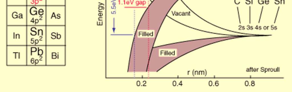
36 Semiconductors INTRINSIC Intrinsic semiconductors are pure materials with the band structure. The number of electrons in the conduction band is determined only by the size of the band gap and the temperature (more electrons with small band gap and high temperature). EXTRINSIC Extrinsic semiconductors are materials where the conductivity is controlled by adding dopants with different numbers of valenece electrons to that of the original material. 36
 the band edges are not aligned so the electron doesn't transit directly to the conduction band.")
37 Semiconductors A direct band gap (InAs, GaAs) the band edges aligned in k, so that a electron can transit from the valence band to the conduction band, with the emission of a photon, without changing considerably the momentum. An indirect band gap (Si, Ge, AlSb) the band edges are not aligned so the electron doesn't transit directly to the conduction band. In this process both a photon and a phonon are involved. 37
38 38
39 39
40 Two fundamental differences between extrinsic and intrinsic semiconductors: 1) At standard temperatures extrinsic semiconductors tend to have significantly greater conductivities than comparable intrinsic ones. 2) The conductivity of an extrinsic semiconductor can easily and accurately be controlled by controlling the amount of dopant. Materials can be manufactured to exact specifications of conductivity. 40
41 Metals T > 0 E C Valence band E F E = 0 41
42 Insulators T > 0 Conduction E C E gap E F Valence band E V 42
43 Intrinsic Semiconductors T > 0 Conduction Valence band E F E C E V 43
44 Extrinsic Semiconductors 44
45 Extrinsic Semiconductors Doping of semiconductors - introducing atoms with more or less electrons than the parent element. Doping is substitutional, the dopant atoms directly replace the original atoms. Very low levels of dopant are required, only 1 atom in 10 9 of the parent atoms. 45
46 Extrinsic Semiconductors n-type n-type Si E C E F E D E V E gap ~ 1 ev 46
47 Extrinsic Semiconductors n-type Silicon - phosphorous atoms introduce extra electrons (one extra valence electron for each dopant atom introduced as P) The dopant atoms form a set of energy levels that lie in the band gap between the valence and conduction bands, but close to the conduction band. The electrons in the dopant levels cannot move directly - there is not enough of them to form a continuous band. The levels act as donor levels because the electrons have enough thermal energy to get up into the conduction band where they can move freely. n-type semiconductors, the negative charge carriers or electrons. 47
48 Extrinsic Semiconductors p-type E C E F E V p-type Si E A 48
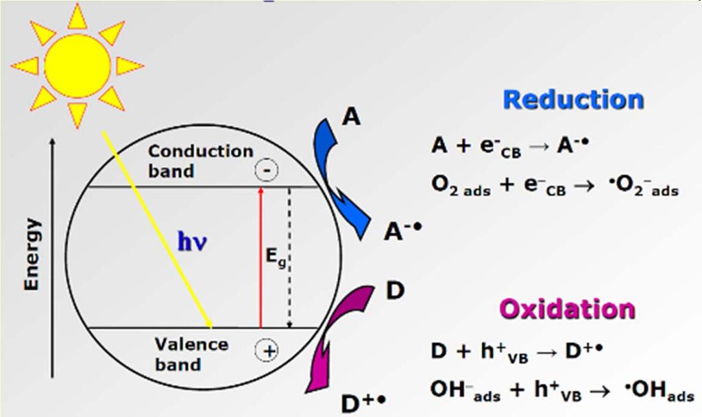
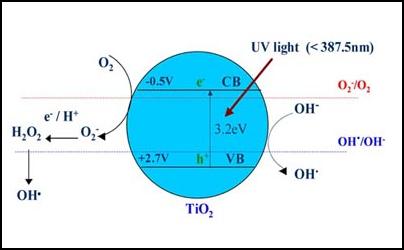
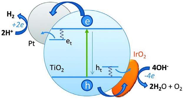
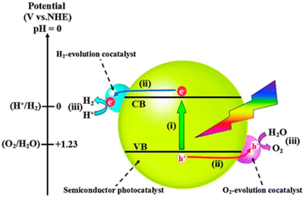
49 Extrinsic Semiconductors p-type Doping with an element with one less valence electron such as Ga For every dopant atom - an electron missing, form a narrow, empty band consisting of acceptor levels which lie just above the valence band, discrete levels if the concentration of gallium atoms is small. Electrons from the valence band have enough thermal energy to be promoted into the acceptor levels, electrons in the acceptor levels cannot contribute to the conductivity of the material. The positive holes in the valence band left behind by the promoted electrons are able to move - p-type semiconductors, the positive holes. 49
50 50
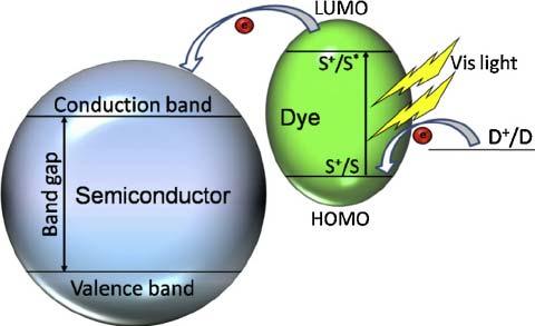
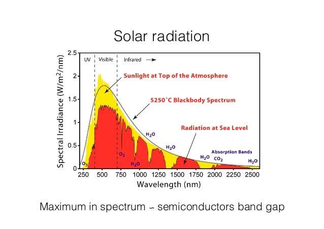
51 Controlled Valency Semiconductors Some transition metal compounds can be conductors due to the presence of an element in more than one oxidation state. NiO On oxidation - turns black and becomes a relatively good conductor Some of the Ni 2+ ions oxidized to Ni 3+ and some Ni 2+ ions diffuse out to maintain charge balance leaving cation holes. The reason for the conduction is the ability of electrons to transfer from Ni 2+ to Ni 3+ ions. This basically allows the Ni 3+ ions to move and black NiO is therefore a p-type semiconductor. 51
52 The transfer process is thermally controlled and therefore highly dependent on temperature, makes controlling the conductivity difficult. Controlled valency semiconductors rely on control of the concentration of Ni 3+ ions by controlled addition of a dopant (such as lithium). NiO Li + x Ni x Ni 3+ x O Hopping Semiconductor the concentration of Li + ions controls the conductivity 52
53 Delocalized Bands Localized Bonds Molecules: Mulliken overlap population Σ 2 c 1 c 2 S 12 c 1, c 2 same sign = bonding c 1, c 2 opposite sign = antibonding S 12 overlap integral Solids: Overlap population-weighted density of states = crystal orbital overlap population (COOP) for a specific bond COOP curves Sign positive = bonding, negative = antibonding Amplitude depends on DOS, orbital overlap, MO coefficients 53
54 DOS and COOP for the Ti-O bonds in rutile 54
55 DOS and COOP for the Ni-Ni bonds in Ni metal 55
56 Peierls distortion 56

57 Peierls distortion maximizing bonding, lowering the DOS at the Fermi level, bonding states down in energy, antibonding states up, a band gap opens at the Fermi level Destabilization Stabilization 57
58 Peierls distortion 58
59 Photocatalysis 59
60 Photocatalysis 60

61 Solar cells 61
The electronic structure of solids. Charge transport in solids
 The electronic structure of solids We need a picture of the electronic structure of solid that we can use to explain experimental observations and make predictions Why is diamond an insulator? Why is sodium
Chapter 4: Bonding in Solids and Electronic Properties. Free electron theory
 Chapter 4: Bonding in Solids and Electronic Properties Free electron theory Consider free electrons in a metal an electron gas. regards a metal as a box in which electrons are free to move. assumes nuclei
Introduction to Engineering Materials ENGR2000. Dr.Coates
 Introduction to Engineering Materials ENGR2000 Chapter 18: Electrical Properties Dr.Coates 18.2 Ohm s Law V = IR where R is the resistance of the material, V is the voltage and I is the current. l R A
CME 300 Properties of Materials. ANSWERS: Homework 9 November 26, As atoms approach each other in the solid state the quantized energy states:
 CME 300 Properties of Materials ANSWERS: Homework 9 November 26, 2011 As atoms approach each other in the solid state the quantized energy states: are split. This splitting is associated with the wave
Chem 241. Lecture 21. UMass Amherst Biochemistry... Teaching Initiative
 Chem 241 Lecture 21 UMass Amherst Biochemistry... Teaching Initiative Announcement March 26 Second Exam Recap Calculation of space filling Counting atoms Alloys Ionic Solids Rock Salt CsCl... 2 ZnS Sphalerite/
Ch. 2: Energy Bands And Charge Carriers In Semiconductors
 Ch. 2: Energy Bands And Charge Carriers In Semiconductors Discrete energy levels arise from balance of attraction force between electrons and nucleus and repulsion force between electrons each electron
Free Electron Model for Metals
 Free Electron Model for Metals Metals are very good at conducting both heat and electricity. A lattice of in a sea of electrons shared between all nuclei (moving freely between them): This is referred
Chapter 1 Overview of Semiconductor Materials and Physics
 Chapter 1 Overview of Semiconductor Materials and Physics Professor Paul K. Chu Conductivity / Resistivity of Insulators, Semiconductors, and Conductors Semiconductor Elements Period II III IV V VI 2 B
Semiconductor Physics and Devices Chapter 3.
 Introduction to the Quantum Theory of Solids We applied quantum mechanics and Schrödinger s equation to determine the behavior of electrons in a potential. Important findings Semiconductor Physics and
Electrons, Holes, and Defect ionization
 Electrons, Holes, and Defect ionization The process of forming intrinsic electron-hole pairs is excitation a cross the band gap ( formation energy ). intrinsic electronic reaction : null e + h When electrons
Basic cell design. Si cell
 Basic cell design Si cell 1 Concepts needed to describe photovoltaic device 1. energy bands in semiconductors: from bonds to bands 2. free carriers: holes and electrons, doping 3. electron and hole current:
Free Electron Model for Metals
 Free Electron Model for Metals Metals are very good at conducting both heat and electricity. A lattice of in a sea of electrons shared between all nuclei (moving freely between them): This is referred
Chemistry Instrumental Analysis Lecture 8. Chem 4631
 Chemistry 4631 Instrumental Analysis Lecture 8 UV to IR Components of Optical Basic components of spectroscopic instruments: stable source of radiant energy transparent container to hold sample device
A semiconductor is an almost insulating material, in which by contamination (doping) positive or negative charge carriers can be introduced.
 positive or negative charge carriers can be introduced.") Semiconductor A semiconductor is an almost insulating material, in which by contamination (doping) positive or negative charge carriers can be introduced. Page 2 Semiconductor materials Page 3 Energy levels
Semiconductor A semiconductor is an almost insulating material, in which by contamination (doping) positive or negative charge carriers can be introduced. Page 2 Semiconductor materials Page 3 Energy levels
CH676 Physical Chemistry: Principles and Applications. CH676 Physical Chemistry: Principles and Applications
 CH676 Physical Chemistry: Principles and Applications Crystal Structure: XRD XRD: Diffraction Peak Positions Centering Allowed Peaks I-centered h+k+l is an even number F-centered hkl either all even or
4.2 Molecular orbitals and atomic orbitals Consider a linear chain of four identical atoms representing a hypothetical molecule.
 4. Molecular orbitals and atomic orbitals Consider a linear chain of four identical atoms representing a hypothetical molecule. Suppose that each atomic wavefunction is 1s wavefunction. This system of
Ionic Bonding. Example: Atomic Radius: Na (r = 0.192nm) Cl (r = 0.099nm) Ionic Radius : Na (r = 0.095nm) Cl (r = 0.181nm)
 Cl (r = 0.099nm) Ionic Radius : Na (r = 0.095nm) Cl (r = 0.181nm)") Ionic Bonding Ion: an atom or molecule that gains or loses electrons (acquires an electrical charge). Atoms form cations (+charge), when they lose electrons, or anions (- charge), when they gain electrons.
Ionic Bonding Ion: an atom or molecule that gains or loses electrons (acquires an electrical charge). Atoms form cations (+charge), when they lose electrons, or anions (- charge), when they gain electrons.
Lecture 7: Extrinsic semiconductors - Fermi level
 Lecture 7: Extrinsic semiconductors - Fermi level Contents 1 Dopant materials 1 2 E F in extrinsic semiconductors 5 3 Temperature dependence of carrier concentration 6 3.1 Low temperature regime (T < T
Charge Carriers in Semiconductor
 Charge Carriers in Semiconductor To understand PN junction s IV characteristics, it is important to understand charge carriers behavior in solids, how to modify carrier densities, and different mechanisms
ENERGY BANDS AND GAPS IN SEMICONDUCTOR. Muhammad Hafeez Javed
 ENERGY BANDS AND GAPS IN SEMICONDUCTOR Muhammad Hafeez Javed www.rmhjaved.com rmhjaved@gmail.com Out Line Introduction Energy band Classification of materials Direct and indirect band gap of SC Classification
EECS130 Integrated Circuit Devices
 EECS130 Integrated Circuit Devices Professor Ali Javey 8/30/2007 Semiconductor Fundamentals Lecture 2 Read: Chapters 1 and 2 Last Lecture: Energy Band Diagram Conduction band E c E g Band gap E v Valence
Semiconductors 1. Explain different types of semiconductors in detail with necessary bond diagrams. Intrinsic semiconductors:
 Semiconductors 1. Explain different types of semiconductors in detail with necessary bond diagrams. There are two types of semi conductors. 1. Intrinsic semiconductors 2. Extrinsic semiconductors Intrinsic
CLASS 12th. Semiconductors
 CLASS 12th Semiconductors 01. Distinction Between Metals, Insulators and Semi-Conductors Metals are good conductors of electricity, insulators do not conduct electricity, while the semiconductors have
EE143 Fall 2016 Microfabrication Technologies. Evolution of Devices
 EE143 Fall 2016 Microfabrication Technologies Prof. Ming C. Wu wu@eecs.berkeley.edu 511 Sutardja Dai Hall (SDH) 1-1 Evolution of Devices Yesterday s Transistor (1947) Today s Transistor (2006) 1-2 1 Why
MO s in one-dimensional arrays of like orbitals
 MO s in one-dimensional arrays of like orbitals There will be as many MO s as orbitals in the array. Every molecular orbital is characterized by a specific pattern of nodes, The lowest energy orbital will
Review of Semiconductor Fundamentals
 ECE 541/ME 541 Microelectronic Fabrication Techniques Review of Semiconductor Fundamentals Zheng Yang (ERF 3017, email: yangzhen@uic.edu) Page 1 Semiconductor A semiconductor is an almost insulating material,
Microscopic Ohm s Law
 Microscopic Ohm s Law Outline Semiconductor Review Electron Scattering and Effective Mass Microscopic Derivation of Ohm s Law 1 TRUE / FALSE 1. Judging from the filled bands, material A is an insulator.
Diamond. Covalent Insulators and Semiconductors. Silicon, Germanium, Gray Tin. Chem 462 September 24, 2004
 Covalent Insulators and Chem 462 September 24, 2004 Diamond Pure sp 3 carbon All bonds staggered- ideal d(c-c) - 1.54 Å, like ethane Silicon, Germanium, Gray Tin Diamond structure Si and Ge: semiconductors
Chem 241. Lecture 23. UMass Amherst Biochemistry... Teaching Initiative
 Chem 241 Lecture 23 UMass Amherst Biochemistry... Teaching Initiative Announcement Mistake we have class on the 3 rd not 4 th Exam 3 Originally scheduled April 23 rd (Friday) What about April 26 th (Next
Electrical Properties
 Electrical Properties Electrical Conduction R Ohm s law V = IR I l Area, A V where I is current (Ampere), V is voltage (Volts) and R is the resistance (Ohms or ) of the conductor Resistivity Resistivity,
General Chemistry I (2012) Lecture by B. H. Hong
 Lecture by B. H. Hong") 3.8 The Limitations of Lewis's Theory 3.9 Molecular Orbitals The valence-bond (VB) and molecular orbital (MO) theories are both procedures for constructing approximate wavefunctions of electrons. The MO
3.8 The Limitations of Lewis's Theory 3.9 Molecular Orbitals The valence-bond (VB) and molecular orbital (MO) theories are both procedures for constructing approximate wavefunctions of electrons. The MO
per unit cell Motif: Re at (0, 0, 0); 3O at ( 1 / 2, 0), (0, 0, 1 / 2 ) Re: 6 (octahedral coordination) O: 2 (linear coordination) ReO 6
; 3O at ( 1 / 2, 0), (0, 0, 1 / 2 ) Re: 6 (octahedral coordination) O: 2 (linear coordination) ReO 6") Lattice: Primitive Cubic 1ReO 3 per unit cell Motif: Re at (0, 0, 0); 3O at ( 1 / 2, 0, 0), (0, 1 / 2, 0), (0, 0, 1 / 2 ) Re: 6 (octahedral coordination) O: 2 (linear coordination) ReO 6 octahedra share
Lattice: Primitive Cubic 1ReO 3 per unit cell Motif: Re at (0, 0, 0); 3O at ( 1 / 2, 0, 0), (0, 1 / 2, 0), (0, 0, 1 / 2 ) Re: 6 (octahedral coordination) O: 2 (linear coordination) ReO 6 octahedra share
Lecture 2 Electrons and Holes in Semiconductors
 EE 471: Transport Phenomena in Solid State Devices Spring 2018 Lecture 2 Electrons and Holes in Semiconductors Bryan Ackland Department of Electrical and Computer Engineering Stevens Institute of Technology
Introduction to Semiconductor Physics. Prof.P. Ravindran, Department of Physics, Central University of Tamil Nadu, India
 Introduction to Semiconductor Physics 1 Prof.P. Ravindran, Department of Physics, Central University of Tamil Nadu, India http://folk.uio.no/ravi/cmp2013 Review of Semiconductor Physics Semiconductor fundamentals
Chem 241. Lecture 24. UMass Amherst Biochemistry... Teaching Initiative
 Chem 241 Lecture 24 UMass Amherst Biochemistry... Teaching Initiative Announcement Mistake we have class on the 3 rd not 4 th Exam 3 Originally scheduled April 23 rd (Friday) What about April 26 th (Next
Solid State Device Fundamentals
 Solid State Device Fundamentals ENS 345 Lecture Course by Alexander M. Zaitsev alexander.zaitsev@csi.cuny.edu Tel: 718 982 2812 Office 4N101b 1 The free electron model of metals The free electron model
Calculating Band Structure
 Calculating Band Structure Nearly free electron Assume plane wave solution for electrons Weak potential V(x) Brillouin zone edge Tight binding method Electrons in local atomic states (bound states) Interatomic
EECS143 Microfabrication Technology
 EECS143 Microfabrication Technology Professor Ali Javey Introduction to Materials Lecture 1 Evolution of Devices Yesterday s Transistor (1947) Today s Transistor (2006) Why Semiconductors? Conductors e.g
Electron Energy, E E = 0. Free electron. 3s Band 2p Band Overlapping energy bands. 3p 3s 2p 2s. 2s Band. Electrons. 1s ATOM SOLID.
 Electron Energy, E Free electron Vacuum level 3p 3s 2p 2s 2s Band 3s Band 2p Band Overlapping energy bands Electrons E = 0 1s ATOM 1s SOLID In a metal the various energy bands overlap to give a single
Energy bands in solids. Some pictures are taken from Ashcroft and Mermin from Kittel from Mizutani and from several sources on the web.
 Energy bands in solids Some pictures are taken from Ashcroft and Mermin from Kittel from Mizutani and from several sources on the web. we are starting to remind p E = = mv 1 2 = k mv = 2 2 k 2m 2 Some
Lecture 1. OUTLINE Basic Semiconductor Physics. Reading: Chapter 2.1. Semiconductors Intrinsic (undoped) silicon Doping Carrier concentrations
 silicon Doping Carrier concentrations") Lecture 1 OUTLINE Basic Semiconductor Physics Semiconductors Intrinsic (undoped) silicon Doping Carrier concentrations Reading: Chapter 2.1 EE105 Fall 2007 Lecture 1, Slide 1 What is a Semiconductor? Low
Lecture 1 OUTLINE Basic Semiconductor Physics Semiconductors Intrinsic (undoped) silicon Doping Carrier concentrations Reading: Chapter 2.1 EE105 Fall 2007 Lecture 1, Slide 1 What is a Semiconductor? Low
Bonding in solids The interaction of electrons in neighboring atoms of a solid serves the very important function of holding the crystal together.
 Bonding in solids The interaction of electrons in neighboring atoms of a solid serves the very important function of holding the crystal together. For example Nacl In the Nacl lattice, each Na atom is
Three Most Important Topics (MIT) Today
 Today") Three Most Important Topics (MIT) Today Electrons in periodic potential Energy gap nearly free electron Bloch Theorem Energy gap tight binding Chapter 1 1 Electrons in Periodic Potential We now know the
Three Most Important Topics (MIT) Today Electrons in periodic potential Energy gap nearly free electron Bloch Theorem Energy gap tight binding Chapter 1 1 Electrons in Periodic Potential We now know the
Mat E 272 Lecture 25: Electrical properties of materials
 Mat E 272 Lecture 25: Electrical properties of materials December 6, 2001 Introduction: Calcium and copper are both metals; Ca has a valence of +2 (2 electrons per atom) while Cu has a valence of +1 (1
Chapter 3. Crystal Binding
 Chapter 3. Crystal Binding Energy of a crystal and crystal binding Cohesive energy of Molecular crystals Ionic crystals Metallic crystals Elasticity What causes matter to exist in three different forms?
* motif: a single or repeated design or color
 Chapter 2. Structure A. Electronic structure vs. Geometric structure B. Clean surface vs. Adsorbate covered surface (substrate + overlayer) C. Adsorbate structure - how are the adsorbed molecules bound
So why is sodium a metal? Tungsten Half-filled 5d band & half-filled 6s band. Insulators. Interaction of metals with light?
 Bonding in Solids: Metals, Insulators, & CHEM 107 T. Hughbanks Delocalized bonding in Solids Think of a pure solid as a single, very large molecule. Use our bonding pictures to try to understand properties.
Minimal Update of Solid State Physics
 Minimal Update of Solid State Physics It is expected that participants are acquainted with basics of solid state physics. Therefore here we will refresh only those aspects, which are absolutely necessary
LN 3 IDLE MIND SOLUTIONS
 IDLE MIND SOLUTIONS 1. Let us first look in most general terms at the optical properties of solids with band gaps (E g ) of less than 4 ev, semiconductors by definition. The band gap energy (E g ) can
R measurements (resistivity, magnetoresistance, Hall). Makariy A. Tanatar
. Makariy A. Tanatar") R measurements (resistivity, magnetoresistance, Hall). 590B Makariy A. Tanatar April 18, 2014 Resistivity Typical resistivity temperature dependence: metals, semiconductors Magnetic scattering Resistivities
R measurements (resistivity, magnetoresistance, Hall). 590B Makariy A. Tanatar April 18, 2014 Resistivity Typical resistivity temperature dependence: metals, semiconductors Magnetic scattering Resistivities
The Semiconductor in Equilibrium
 Lecture 6 Semiconductor physics IV The Semiconductor in Equilibrium Equilibrium, or thermal equilibrium No external forces such as voltages, electric fields. Magnetic fields, or temperature gradients are
From Last Time Important new Quantum Mechanical Concepts. Atoms and Molecules. Today. Symmetry. Simple molecules.
 Today From Last Time Important new Quantum Mechanical Concepts Indistinguishability: Symmetries of the wavefunction: Symmetric and Antisymmetric Pauli exclusion principle: only one fermion per state Spin
smal band gap Saturday, April 9, 2011
 small band gap upper (conduction) band empty small gap valence band filled 2s 2p 2s 2p hybrid (s+p)band 2p no gap 2s (depend on the crystallographic orientation) extrinsic semiconductor semi-metal electron
SEMICONDUCTOR PHYSICS
 SEMICONDUCTOR PHYSICS by Dibyendu Chowdhury Semiconductors The materials whose electrical conductivity lies between those of conductors and insulators, are known as semiconductors. Silicon Germanium Cadmium
Semiconductors. SEM and EDAX images of an integrated circuit. SEM EDAX: Si EDAX: Al. Institut für Werkstoffe der ElektrotechnikIWE
 SEM and EDAX images of an integrated circuit SEM EDAX: Si EDAX: Al source: [Cal 99 / 605] M&D-.PPT, slide: 1, 12.02.02 Classification semiconductors electronic semiconductors mixed conductors ionic conductors
ELECTRONIC I Lecture 1 Introduction to semiconductor. By Asst. Prof Dr. Jassim K. Hmood
 ELECTRONIC I Lecture 1 Introduction to semiconductor By Asst. Prof Dr. Jassim K. Hmood SOLID-STATE ELECTRONIC MATERIALS Electronic materials generally can be divided into three categories: insulators,
Bohr s Model, Energy Bands, Electrons and Holes
 Dual Character of Material Particles Experimental physics before 1900 demonstrated that most of the physical phenomena can be explained by Newton's equation of motion of material particles or bodies and
CLASS 1 & 2 REVISION ON SEMICONDUCTOR PHYSICS. Reference: Electronic Devices by Floyd
 CLASS 1 & 2 REVISION ON SEMICONDUCTOR PHYSICS Reference: Electronic Devices by Floyd 1 ELECTRONIC DEVICES Diodes, transistors and integrated circuits (IC) are typical devices in electronic circuits. All
ECE 442. Spring, Lecture -2
 ECE 442 Power Semiconductor Devices and Integrated circuits Spring, 2006 University of Illinois at Chicago Lecture -2 Semiconductor physics band structures and charge carriers 1. What are the types of
Crystal Properties. MS415 Lec. 2. High performance, high current. ZnO. GaN
 Crystal Properties Crystal Lattices: Periodic arrangement of atoms Repeated unit cells (solid-state) Stuffing atoms into unit cells Determine mechanical & electrical properties High performance, high current
Atomic Structure. Atomic weight = m protons + m neutrons Atomic number (Z) = # of protons Isotope corresponds to # of neutrons
 = # of protons Isotope corresponds to # of neutrons") Atomic Structure Neutrons: neutral Protons: positive charge (1.6x10 19 C, 1.67x10 27 kg) Electrons: negative charge (1.6x10 19 C, 9.11x10 31 kg) Atomic weight = m protons + m neutrons Atomic number (Z)
Atomic Structure Neutrons: neutral Protons: positive charge (1.6x10 19 C, 1.67x10 27 kg) Electrons: negative charge (1.6x10 19 C, 9.11x10 31 kg) Atomic weight = m protons + m neutrons Atomic number (Z)
Semiconductor Device Physics
 1 Semiconductor Device Physics Lecture 1 http://zitompul.wordpress.com 2 0 1 3 2 Semiconductor Device Physics Textbook: Semiconductor Device Fundamentals, Robert F. Pierret, International Edition, Addison
Two-dimensional lattice
 1 Two-dimensional lattice a 1 *, k x k x = 0, k y = 0 X M a 2, y a 1, x Γ X a 2 *, k y k x = 0.5 a 1 *, k y = 0 k x = 0, k y = 0.5 a 2 * Γ k x = 0.5 a 1 *, k y = 0.5 a 2 * X X M k x = 0.25 a 1 *, k y =
Lecture 2. Semiconductor Physics. Sunday 4/10/2015 Semiconductor Physics 1-1
 Lecture 2 Semiconductor Physics Sunday 4/10/2015 Semiconductor Physics 1-1 Outline Intrinsic bond model: electrons and holes Charge carrier generation and recombination Intrinsic semiconductor Doping:
Semiconductor Polymer
 Semiconductor Polymer Organic Semiconductor for Flexible Electronics Introduction: An organic semiconductor is an organic compound that possesses similar properties to inorganic semiconductors with hole
MTLE-6120: Advanced Electronic Properties of Materials. Intrinsic and extrinsic semiconductors. Reading: Kasap:
 MTLE-6120: Advanced Electronic Properties of Materials 1 Intrinsic and extrinsic semiconductors Reading: Kasap: 5.1-5.6 Band structure and conduction 2 Metals: partially filled band(s) i.e. bands cross
Semiconductor Physics. Lecture 3
 Semiconductor Physics Lecture 3 Intrinsic carrier density Intrinsic carrier density Law of mass action Valid also if we add an impurity which either donates extra electrons or holes the number of carriers
3. Two-dimensional systems
 3. Two-dimensional systems Image from IBM-Almaden 1 Introduction Type I: natural layered structures, e.g., graphite (with C nanostructures) Type II: artificial structures, heterojunctions Great technological
Molecular Orbital Theory This means that the coefficients in the MO will not be the same!
 Diatomic molecules: Heteronuclear molecules In heteronuclear diatomic molecules, the relative contribution of atomic orbitals to each MO is not equal. Some MO s will have more contribution from AO s on
V, I, R measurements: how to generate and measure quantities and then how to get data (resistivity, magnetoresistance, Hall). Makariy A.
. Makariy A.") V, I, R measurements: how to generate and measure quantities and then how to get data (resistivity, magnetoresistance, Hall). 590B Makariy A. Tanatar November 12, 2008 Resistivity Typical resistivity temperature
V, I, R measurements: how to generate and measure quantities and then how to get data (resistivity, magnetoresistance, Hall). 590B Makariy A. Tanatar November 12, 2008 Resistivity Typical resistivity temperature
Lecture 2: Bonding in solids
 Lecture 2: Bonding in solids Electronegativity Van Arkel-Ketalaar Triangles Atomic and ionic radii Band theory of solids Molecules vs. solids Band structures Analysis of chemical bonds in Reciprocal space
Lecture 4: Band theory
 Lecture 4: Band theory Very short introduction to modern computational solid state chemistry Band theory of solids Molecules vs. solids Band structures Analysis of chemical bonding in Reciprocal space
From Last Time. Several important conceptual aspects of quantum mechanics Indistinguishability. Symmetry
 From Last Time Several important conceptual aspects of quantum mechanics Indistinguishability particles are absolutely identical Leads to Pauli exclusion principle (one Fermion / quantum state). Symmetry
I. Introduction II. Solid State Physics Detection of Light Bernhard Brandl 1
 Detection of Light I. Introduction II. Solid State Physics 4-2-2015 Detection of Light Bernhard Brandl 1 4-2-2015 Detection of Light Bernhard Brandl 2 Blabla Recommended 4-2-2015 Detection of Light Bernhard
Electronics The basics of semiconductor physics
 Electronics The basics of semiconductor physics Prof. Márta Rencz, Gergely Nagy BME DED September 16, 2013 The basic properties of semiconductors Semiconductors conductance is between that of conductors
ECE 250 Electronic Devices 1. Electronic Device Modeling
 ECE 250 Electronic Devices 1 ECE 250 Electronic Device Modeling ECE 250 Electronic Devices 2 Introduction to Semiconductor Physics You should really take a semiconductor device physics course. We can only
Week 13 MO Theory, Solids, & metals
 Week 13 MO Theory, Solids, & metals Q UEST IO N 1 Using the molecular orbital energy diagrams below, which one of the following diatomic molecules is LEAST likely to exist? A. Li2 B. Be2 C. B2 D. C2 E.
EE 346: Semiconductor Devices
 EE 346: Semiconductor Devices Lecture - 6 02/06/2017 Tewodros A. Zewde 1 DENSTY OF STATES FUNCTON Since current is due to the flow of charge, an important step in the process is to determine the number
Solids. properties & structure
 Solids properties & structure Determining Crystal Structure crystalline solids have a very regular geometric arrangement of their particles the arrangement of the particles and distances between them is
Chapter Two. Energy Bands and Effective Mass
 Chapter Two Energy Bands and Effective Mass Energy Bands Formation At Low Temperature At Room Temperature Valence Band Insulators Metals Effective Mass Energy-Momentum Diagrams Direct and Indirect Semiconduction
Atoms? All matters on earth made of atoms (made up of elements or combination of elements).
.") Chapter 1 Atoms? All matters on earth made of atoms (made up of elements or combination of elements). Atomic Structure Atom is the smallest particle of an element that can exist in a stable or independent
Chapter 1 Atoms? All matters on earth made of atoms (made up of elements or combination of elements). Atomic Structure Atom is the smallest particle of an element that can exist in a stable or independent
Review of Optical Properties of Materials
 Review of Optical Properties of Materials Review of optics Absorption in semiconductors: qualitative discussion Derivation of Optical Absorption Coefficient in Direct Semiconductors Photons When dealing
Semiconductors and Optoelectronics. Today Semiconductors Acoustics. Tomorrow Come to CH325 Exercises Tours
 Semiconductors and Optoelectronics Advanced Physics Lab, PHYS 3600 Don Heiman, Northeastern University, 2017 Today Semiconductors Acoustics Tomorrow Come to CH325 Exercises Tours Semiconductors and Optoelectronics
ESE 372 / Spring 2013 / Lecture 5 Metal Oxide Semiconductor Field Effect Transistor
 Metal Oxide Semiconductor Field Effect Transistor V G V G 1 Metal Oxide Semiconductor Field Effect Transistor We will need to understand how this current flows through Si What is electric current? 2 Back
ELEC 4700 Assignment #2
 ELEC 4700 Assignment #2 Question 1 (Kasop 4.2) Molecular Orbitals and Atomic Orbitals Consider a linear chain of four identical atoms representing a hypothetical molecule. Suppose that each atomic wavefunction
Lecture contents. A few concepts from Quantum Mechanics. Tight-binding model Solid state physics review
 Lecture contents A few concepts from Quantum Mechanics Particle in a well Two wells: QM perturbation theory Many wells (atoms) BAND formation Tight-binding model Solid state physics review Approximations
Classification of Solids
 Classification of Solids Classification by conductivity, which is related to the band structure: (Filled bands are shown dark; D(E) = Density of states) Class Electron Density Density of States D(E) Examples
We have arrived to the question: how do molecular bonds determine the band gap? We have discussed that the silicon atom has four outer electrons.
 ET3034Tux - 2.2.2 - Band Gap 2 - Electrons in Molecular Bonds We have arrived to the question: how do molecular bonds determine the band gap? We have discussed that the silicon atom has four outer electrons.
 lectures accompanying the book: Solid State Physics: An Introduction, by Philip ofmann (2nd edition 2015, ISBN-10: 3527412824, ISBN-13: 978-3527412822, Wiley-VC Berlin. www.philiphofmann.net 1 Bonds between
CHAPTER 2: ENERGY BANDS & CARRIER CONCENTRATION IN THERMAL EQUILIBRIUM. M.N.A. Halif & S.N. Sabki
 CHAPTER 2: ENERGY BANDS & CARRIER CONCENTRATION IN THERMAL EQUILIBRIUM OUTLINE 2.1 INTRODUCTION: 2.1.1 Semiconductor Materials 2.1.2 Basic Crystal Structure 2.1.3 Basic Crystal Growth technique 2.1.4 Valence
Electrons and Molecular Forces
 Electrons and Molecular Forces Chemistry 30 Ms. Hayduk Electron Configuration Atomic Structure Atomic Number Number of protons in the nucleus Defines the element Used to organize the periodic table 1 Bohr
Electronic Structure of Surfaces
 Electronic Structure of Surfaces When solids made of an infinite number of atoms are formed, it is a common misconception to consider each atom individually. Rather, we must consider the structure of the
Metallic & Ionic Solids. Crystal Lattices. Properties of Solids. Network Solids. Types of Solids. Chapter 13 Solids. Chapter 13
 1 Metallic & Ionic Solids Chapter 13 The Chemistry of Solids Jeffrey Mack California State University, Sacramento Crystal Lattices Properties of Solids Regular 3-D arrangements of equivalent LATTICE POINTS
Semiconductors. Semiconductors also can collect and generate photons, so they are important in optoelectronic or photonic applications.
 Semiconductors Semiconducting materials have electrical properties that fall between true conductors, (like metals) which are always highly conducting and insulators (like glass or plastic or common ceramics)
Semiconductor physics I. The Crystal Structure of Solids
 Lecture 3 Semiconductor physics I The Crystal Structure of Solids 1 Semiconductor materials Types of solids Space lattices Atomic Bonding Imperfection and doping in SOLIDS 2 Semiconductor Semiconductors
Two-dimensional lattice
 Two-dimensional lattice a 1 *, k x k x =0,k y =0 X M a 2, y Γ X a 2 *, k y a 1, x Reciprocal lattice Γ k x = 0.5 a 1 *, k y =0 k x = 0, k y = 0.5 a 2 * k x =0.5a 1 *, k y =0.5a 2 * X X M k x = 0.25 a 1
What happens when substances freeze into solids? Less thermal energy available Less motion of the molecules More ordered spatial properties
 Chapter #16 Liquids and Solids 16.1) Intermolecular Forces 16.2) The Liquid State 16.3) An Introduction to Structures and Types of Solids 16.4) Structure and Bonding of Metals 16.5) Carbon and Silicon:
Modern Physics for Frommies IV The Universe - Small to Large Lecture 4
 Fromm Institute for Lifelong Learning University of San Francisco Modern Physics for Frommies IV The Universe - Small to Large Lecture 4 3 February 06 Modern Physics IV Lecture 4 Agenda Administrative
Course overview. Me: Dr Luke Wilson. The course: Physics and applications of semiconductors. Office: E17 open door policy
 Course overview Me: Dr Luke Wilson Office: E17 open door policy email: luke.wilson@sheffield.ac.uk The course: Physics and applications of semiconductors 10 lectures aim is to allow time for at least one
Engineering 2000 Chapter 8 Semiconductors. ENG2000: R.I. Hornsey Semi: 1
 Engineering 2000 Chapter 8 Semiconductors ENG2000: R.I. Hornsey Semi: 1 Overview We need to know the electrical properties of Si To do this, we must also draw on some of the physical properties and we