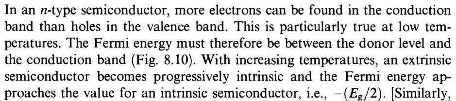
smal band gap Saturday, April 9, 2011
|
|
|
- Hope Booth
- 5 years ago
- Views:
Transcription
1
2 small band gap
3 upper (conduction) band empty small gap valence band filled

4 2s 2p 2s 2p hybrid (s+p)band

5 2p no gap 2s
6 (depend on the crystallographic orientation) extrinsic semiconductor semi-metal
7

8 electron hole
9 reference energy T>0K average Fermi Energy (between F(E)=0 and F(E)=1 100% filled T=0K
10 Recall, Population density (for energy above EF) = at room temperature
11 (number of conduction electrons between E and E+dE above EF or Ec ) (bottom of conduction band)
12
13 At room temperature, Ne~10 9 / cm 3 1cm 3 ~10 22 Si atoms only one in every atoms contributes an electron to conduction band ~poor conductivity
14 Mobility, μ
15 more electrons to conduction band
16 intrinsic semi-conductor, very small amount of electrons in conduction band 10 9 /cm 3 extrinsic semi-conductor, by doping elements form III and V groups n type semi-conductor, donor impurities (P, As, Sb) major carrier: electrons p type semi-conductor, acceptor impurities (B, Al, Ga, In) major carrier: holes
17 (1) the bonding energy of Si to the fifth (extra) electron is 0.045eV. (2) more electrons in valence bands are excited to conduction band ~the number of conduction electron increases
 level (2) acceptor")
18 of extrinsic semiconductor (1) donor(extra) level (2) acceptor (extra) level
 donor band")
19 (2) donor band empty (1) donor band filled
20 p-type semiconductor with increasing temperature, the electrons are excited to acceptor band Np (2) acceptor band filled (1) acceptor band empty
21 of extrinsic semiconductor At room temperature, Ne(intrinsic) is very small, Nde>>Ne(intrinsic) Nde~Nd (number of doping atoms) depends on the doping level like metals number of carrier increase (semiconductor)
22 Conductivity of Metals at high temperature, the phonon scattering dominates σ measure the conductivity of material at very low temperature, we know the behavior of metal or semiconductor
23 temperature dependent

24 (measure types and number of charge carriers) n-type dopant electron deficient electron accumulates Hall field builds up
25 Hall constant, Hall constant is negative for electron carrier
26 III-V GaAs GaP GaN InP InAs InSb II-VI ZnO ZnS ZnSe CdS CdTe HgS GaAs ~ direct band gap ~ high speed device large electron mobility smaller effective mass ~ Laser/ LED (Optical Application) ~ high frequency device Tele-communication military applications, Satellite Pre-amplifier
27
 (space")
28 As + n-type p-type repel electrons negative bias positive bias repel holes (space charge) (space charge)
29
30 ionization energy
31
32
33
34
35
36
37 Photoelectric effect and Solar cell of Metal Photon in > Electron out

38 Work function and Fermi energy (Metal) Φ Ef: the highest energy of the occupied levels at 0K

39 Work function of Metals In general, the work function of metals is between 3~5 ev
40 Photoelectric Effect and Solar Cell of Metal photon Φ Voc Isc
41 Photoelectric Effect and Solar Cell of Metal 3 5eV - 1% 0.001% (photovoltaic)
42 Photovoltaic effect of Semiconductor Photon in > Electron out 1~2eV - ( )

43 Some semiconductor physics a) Band structure and Doping when silicon is doped with group 5 impurity atoms (for example, phosphorus) which are called donnors. this doping creates extra electron in this band. The extra electrons - called electrons A semiconductor where the electric current is carried predominantly by electrons is called n-type when silicon is doped with group 3 impurity atoms (for example, boron) which are called acceptors. this doping creates electron deficiency in this band. The missing electrons - called holes A semiconductor where the electric current is carried predominantly by holes is called p-type
44


45 Some semiconductor physics b) Semiconductor Junction space charge The potential barrier of a junction permits the flow of electric current in only one direction - the junction acts as a rectifier, or diode. This can be seen in our example where electrons can only flow from the p region to the n region, and holes can only flow in the opposite direction. Electric current, which is the sum of the two, can therefore flow only from the p-side to the n-side of the junction (remember that it is defined as the direction of flow of the positive carriers!)


46 Some semiconductor physics c) Light absorption by a semiconductor = generation Only some of these photons - those with energy in excess of the bandgap - can be converted into electricity by the solar cell. Each semiconductor is restricted to converting only a part of the solar spectrum.
47 How a p-n junction solar cells work?
48 How a p-n junction solar cells work?
49 How a p-n junction solar cells work?
50 How a p-n junction solar cells work?


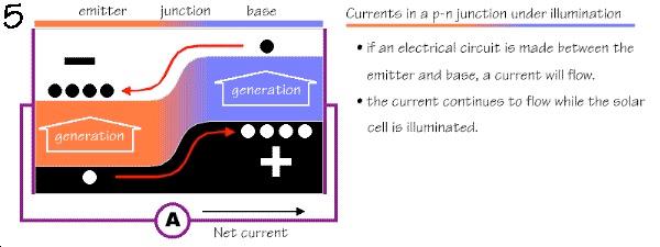
51 How a p-n junction solar cells work? photo-current (emitter--> base)
52 How solar cells work? (space charge) Metal-semiconductor contact) Ec Ev Eg Immediately after their creation, the electron and hole decay to states near the edges of their respective bands. The excess energy is lost as heat and cannot be converted into useful power. This represents one of the fundamental loss mechanisms in a solar cell.

 that supply current to a larger bus bar.")
53 How solar cells work? This diagram shows a typical crystalline silicon solar cell. The electrical current generated in the semiconductor is extracted by contacts to the front and rear of the cell. The top contact structure which must allow light to pass through is made in the form of widely-spaced thin metal strips (usually called fingers) that supply current to a larger bus bar. The cell is covered with a thin layer of dielectric material - the anti-reflection coating, ARC (Si3N4)- to minimize light reflection from the top surface.

54 diode solar cell photo-current

55 (space charge) Metal-semiconductor contact) η=pmax/ Most frequent conditions are: irradiance 100 mw/cm 2, standard
56 Efficiency of Solar Cell
Chemistry Instrumental Analysis Lecture 8. Chem 4631
 Chemistry 4631 Instrumental Analysis Lecture 8 UV to IR Components of Optical Basic components of spectroscopic instruments: stable source of radiant energy transparent container to hold sample device
Conductivity and Semi-Conductors
 Conductivity and Semi-Conductors J = current density = I/A E = Electric field intensity = V/l where l is the distance between two points Metals: Semiconductors: Many Polymers and Glasses 1 Electrical Conduction
Chapter 1 Overview of Semiconductor Materials and Physics
 Chapter 1 Overview of Semiconductor Materials and Physics Professor Paul K. Chu Conductivity / Resistivity of Insulators, Semiconductors, and Conductors Semiconductor Elements Period II III IV V VI 2 B
Lecture 1. OUTLINE Basic Semiconductor Physics. Reading: Chapter 2.1. Semiconductors Intrinsic (undoped) silicon Doping Carrier concentrations
 silicon Doping Carrier concentrations") Lecture 1 OUTLINE Basic Semiconductor Physics Semiconductors Intrinsic (undoped) silicon Doping Carrier concentrations Reading: Chapter 2.1 EE105 Fall 2007 Lecture 1, Slide 1 What is a Semiconductor? Low
Lecture 1 OUTLINE Basic Semiconductor Physics Semiconductors Intrinsic (undoped) silicon Doping Carrier concentrations Reading: Chapter 2.1 EE105 Fall 2007 Lecture 1, Slide 1 What is a Semiconductor? Low
Semiconductors 1. Explain different types of semiconductors in detail with necessary bond diagrams. Intrinsic semiconductors:
 Semiconductors 1. Explain different types of semiconductors in detail with necessary bond diagrams. There are two types of semi conductors. 1. Intrinsic semiconductors 2. Extrinsic semiconductors Intrinsic
EE143 Fall 2016 Microfabrication Technologies. Evolution of Devices
 EE143 Fall 2016 Microfabrication Technologies Prof. Ming C. Wu wu@eecs.berkeley.edu 511 Sutardja Dai Hall (SDH) 1-1 Evolution of Devices Yesterday s Transistor (1947) Today s Transistor (2006) 1-2 1 Why
EECS130 Integrated Circuit Devices
 EECS130 Integrated Circuit Devices Professor Ali Javey 8/30/2007 Semiconductor Fundamentals Lecture 2 Read: Chapters 1 and 2 Last Lecture: Energy Band Diagram Conduction band E c E g Band gap E v Valence
Basic cell design. Si cell
 Basic cell design Si cell 1 Concepts needed to describe photovoltaic device 1. energy bands in semiconductors: from bonds to bands 2. free carriers: holes and electrons, doping 3. electron and hole current:
Semiconductors. SEM and EDAX images of an integrated circuit. SEM EDAX: Si EDAX: Al. Institut für Werkstoffe der ElektrotechnikIWE
 SEM and EDAX images of an integrated circuit SEM EDAX: Si EDAX: Al source: [Cal 99 / 605] M&D-.PPT, slide: 1, 12.02.02 Classification semiconductors electronic semiconductors mixed conductors ionic conductors
First-Hand Investigation: Modeling of Semiconductors
 perform an investigation to model the behaviour of semiconductors, including the creation of a hole or positive charge on the atom that has lost the electron and the movement of electrons and holes in
EECS143 Microfabrication Technology
 EECS143 Microfabrication Technology Professor Ali Javey Introduction to Materials Lecture 1 Evolution of Devices Yesterday s Transistor (1947) Today s Transistor (2006) Why Semiconductors? Conductors e.g
Basic Semiconductor Physics
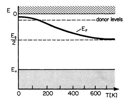
 6 Basic Semiconductor Physics 6.1 Introduction With this chapter we start with the discussion of some important concepts from semiconductor physics, which are required to understand the operation of solar
Lecture 7: Extrinsic semiconductors - Fermi level
 Lecture 7: Extrinsic semiconductors - Fermi level Contents 1 Dopant materials 1 2 E F in extrinsic semiconductors 5 3 Temperature dependence of carrier concentration 6 3.1 Low temperature regime (T < T
EE 346: Semiconductor Devices. 02/08/2017 Tewodros A. Zewde 1
 EE 346: Semiconductor Devices 02/08/2017 Tewodros A. Zewde 1 DOPANT ATOMS AND ENERGY LEVELS Without help the total number of carriers (electrons and holes) is limited to 2ni. For most materials, this is
CLASS 12th. Semiconductors
 CLASS 12th Semiconductors 01. Distinction Between Metals, Insulators and Semi-Conductors Metals are good conductors of electricity, insulators do not conduct electricity, while the semiconductors have
Unit IV Semiconductors Engineering Physics
 Introduction A semiconductor is a material that has a resistivity lies between that of a conductor and an insulator. The conductivity of a semiconductor material can be varied under an external electrical
Crystal Properties. MS415 Lec. 2. High performance, high current. ZnO. GaN
 Crystal Properties Crystal Lattices: Periodic arrangement of atoms Repeated unit cells (solid-state) Stuffing atoms into unit cells Determine mechanical & electrical properties High performance, high current
Charge Carriers in Semiconductor
 Charge Carriers in Semiconductor To understand PN junction s IV characteristics, it is important to understand charge carriers behavior in solids, how to modify carrier densities, and different mechanisms
CME 300 Properties of Materials. ANSWERS: Homework 9 November 26, As atoms approach each other in the solid state the quantized energy states:
 CME 300 Properties of Materials ANSWERS: Homework 9 November 26, 2011 As atoms approach each other in the solid state the quantized energy states: are split. This splitting is associated with the wave
EE 346: Semiconductor Devices
 EE 346: Semiconductor Devices Lecture - 6 02/06/2017 Tewodros A. Zewde 1 DENSTY OF STATES FUNCTON Since current is due to the flow of charge, an important step in the process is to determine the number
EE 446/646 Photovoltaic Devices I. Y. Baghzouz
 EE 446/646 Photovoltaic Devices I Y. Baghzouz What is Photovoltaics? First used in about 1890, the word has two parts: photo, derived from the Greek word for light, volt, relating to electricity pioneer
Ga and P Atoms to Covalent Solid GaP
 Ga and P Atoms to Covalent Solid GaP Band Gaps in Binary Group III-V Semiconductors Mixed Semiconductors Affect of replacing some of the As with P in GaAs Band Gap (ev) (nm) GaAs 1.35 919 (IR) GaP 2.24
Calculating Band Structure
 Calculating Band Structure Nearly free electron Assume plane wave solution for electrons Weak potential V(x) Brillouin zone edge Tight binding method Electrons in local atomic states (bound states) Interatomic
Semiconductors and Optoelectronics. Today Semiconductors Acoustics. Tomorrow Come to CH325 Exercises Tours
 Semiconductors and Optoelectronics Advanced Physics Lab, PHYS 3600 Don Heiman, Northeastern University, 2017 Today Semiconductors Acoustics Tomorrow Come to CH325 Exercises Tours Semiconductors and Optoelectronics
Advantages / Disadvantages of semiconductor detectors
 Advantages / Disadvantages of semiconductor detectors Semiconductor detectors have a high density (compared to gas detector) large energy loss in a short distance diffusion effect is smaller than in gas
A semiconductor is an almost insulating material, in which by contamination (doping) positive or negative charge carriers can be introduced.
 positive or negative charge carriers can be introduced.") Semiconductor A semiconductor is an almost insulating material, in which by contamination (doping) positive or negative charge carriers can be introduced. Page 2 Semiconductor materials Page 3 Energy levels
Semiconductor A semiconductor is an almost insulating material, in which by contamination (doping) positive or negative charge carriers can be introduced. Page 2 Semiconductor materials Page 3 Energy levels
Lecture 2. Semiconductor Physics. Sunday 4/10/2015 Semiconductor Physics 1-1
 Lecture 2 Semiconductor Physics Sunday 4/10/2015 Semiconductor Physics 1-1 Outline Intrinsic bond model: electrons and holes Charge carrier generation and recombination Intrinsic semiconductor Doping:
KATIHAL FİZİĞİ MNT-510
 KATIHAL FİZİĞİ MNT-510 YARIİLETKENLER Kaynaklar: Katıhal Fiziği, Prof. Dr. Mustafa Dikici, Seçkin Yayıncılık Katıhal Fiziği, Şakir Aydoğan, Nobel Yayıncılık, Physics for Computer Science Students: With
Free Electron Model for Metals
 Free Electron Model for Metals Metals are very good at conducting both heat and electricity. A lattice of in a sea of electrons shared between all nuclei (moving freely between them): This is referred
EXTRINSIC SEMICONDUCTOR
 EXTRINSIC SEMICONDUCTOR In an extrinsic semiconducting material, the charge carriers originate from impurity atoms added to the original material is called impurity [or] extrinsic semiconductor. This Semiconductor
Free Electron Model for Metals
 Free Electron Model for Metals Metals are very good at conducting both heat and electricity. A lattice of in a sea of electrons shared between all nuclei (moving freely between them): This is referred
EE495/695 Introduction to Semiconductors I. Y. Baghzouz ECE Department UNLV
 EE495/695 Introduction to Semiconductors I Y. Baghzouz ECE Department UNLV Introduction Solar cells have always been aligned closely with other electronic devices. We will cover the basic aspects of semiconductor
Review of Semiconductor Fundamentals
 ECE 541/ME 541 Microelectronic Fabrication Techniques Review of Semiconductor Fundamentals Zheng Yang (ERF 3017, email: yangzhen@uic.edu) Page 1 Semiconductor A semiconductor is an almost insulating material,
Introduction to Engineering Materials ENGR2000. Dr.Coates
 Introduction to Engineering Materials ENGR2000 Chapter 18: Electrical Properties Dr.Coates 18.2 Ohm s Law V = IR where R is the resistance of the material, V is the voltage and I is the current. l R A
3.1 Introduction to Semiconductors. Y. Baghzouz ECE Department UNLV
 3.1 Introduction to Semiconductors Y. Baghzouz ECE Department UNLV Introduction In this lecture, we will cover the basic aspects of semiconductor materials, and the physical mechanisms which are at the
PHOTOVOLTAICS Fundamentals
 PHOTOVOLTAICS Fundamentals PV FUNDAMENTALS Semiconductor basics pn junction Solar cell operation Design of silicon solar cell SEMICONDUCTOR BASICS Allowed energy bands Valence and conduction band Fermi
Semiconductor Detectors
 Semiconductor Detectors Summary of Last Lecture Band structure in Solids: Conduction band Conduction band thermal conductivity: E g > 5 ev Valence band Insulator Charge carrier in conductor: e - Charge
Chapter 12: Semiconductors
 Chapter 12: Semiconductors Bardeen & Shottky January 30, 2017 Contents 1 Band Structure 4 2 Charge Carrier Density in Intrinsic Semiconductors. 6 3 Doping of Semiconductors 12 4 Carrier Densities in Doped
EE301 Electronics I , Fall
 EE301 Electronics I 2018-2019, Fall 1. Introduction to Microelectronics (1 Week/3 Hrs.) Introduction, Historical Background, Basic Consepts 2. Rewiev of Semiconductors (1 Week/3 Hrs.) Semiconductor materials
Classification of Solids
 Classification of Solids Classification by conductivity, which is related to the band structure: (Filled bands are shown dark; D(E) = Density of states) Class Electron Density Density of States D(E) Examples
LN 3 IDLE MIND SOLUTIONS
 IDLE MIND SOLUTIONS 1. Let us first look in most general terms at the optical properties of solids with band gaps (E g ) of less than 4 ev, semiconductors by definition. The band gap energy (E g ) can
Engineering 2000 Chapter 8 Semiconductors. ENG2000: R.I. Hornsey Semi: 1
 Engineering 2000 Chapter 8 Semiconductors ENG2000: R.I. Hornsey Semi: 1 Overview We need to know the electrical properties of Si To do this, we must also draw on some of the physical properties and we
Note that it is traditional to draw the diagram for semiconductors rotated 90 degrees, i.e. the version on the right above.
 5 Semiconductors The nearly free electron model applies equally in the case where the Fermi level lies within a small band gap (semiconductors), as it does when the Fermi level lies within a band (metal)
Session 5: Solid State Physics. Charge Mobility Drift Diffusion Recombination-Generation
 Session 5: Solid State Physics Charge Mobility Drift Diffusion Recombination-Generation 1 Outline A B C D E F G H I J 2 Mobile Charge Carriers in Semiconductors Three primary types of carrier action occur
ELECTRONIC I Lecture 1 Introduction to semiconductor. By Asst. Prof Dr. Jassim K. Hmood
 ELECTRONIC I Lecture 1 Introduction to semiconductor By Asst. Prof Dr. Jassim K. Hmood SOLID-STATE ELECTRONIC MATERIALS Electronic materials generally can be divided into three categories: insulators,
Course overview. Me: Dr Luke Wilson. The course: Physics and applications of semiconductors. Office: E17 open door policy
 Course overview Me: Dr Luke Wilson Office: E17 open door policy email: luke.wilson@sheffield.ac.uk The course: Physics and applications of semiconductors 10 lectures aim is to allow time for at least one
ELECTRONIC DEVICES AND CIRCUITS SUMMARY
 ELECTRONIC DEVICES AND CIRCUITS SUMMARY Classification of Materials: Insulator: An insulator is a material that offers a very low level (or negligible) of conductivity when voltage is applied. Eg: Paper,
Due to the quantum nature of electrons, one energy state can be occupied only by one electron.
 In crystalline solids, not all values of the electron energy are possible. The allowed intervals of energy are called allowed bands (shown as blue and chess-board blue). The forbidden intervals are called
Ch. 2: Energy Bands And Charge Carriers In Semiconductors
 Ch. 2: Energy Bands And Charge Carriers In Semiconductors Discrete energy levels arise from balance of attraction force between electrons and nucleus and repulsion force between electrons each electron
Lecture 2 Electrons and Holes in Semiconductors
 EE 471: Transport Phenomena in Solid State Devices Spring 2018 Lecture 2 Electrons and Holes in Semiconductors Bryan Ackland Department of Electrical and Computer Engineering Stevens Institute of Technology
Lecture 3b. Bonding Model and Dopants. Reading: (Cont d) Notes and Anderson 2 sections
 Notes and Anderson 2 sections") Lecture 3b Bonding Model and Dopants Reading: (Cont d) Notes and Anderson 2 sections 2.3-2.7 The need for more control over carrier concentration Without help the total number of carriers (electrons and
Lecture 3b Bonding Model and Dopants Reading: (Cont d) Notes and Anderson 2 sections 2.3-2.7 The need for more control over carrier concentration Without help the total number of carriers (electrons and
Semiconductor Devices and Circuits Fall Midterm Exam. Instructor: Dr. Dietmar Knipp, Professor of Electrical Engineering. Name: Mat. -Nr.
 Semiconductor Devices and Circuits Fall 2003 Midterm Exam Instructor: Dr. Dietmar Knipp, Professor of Electrical Engineering Name: Mat. -Nr.: Guidelines: Duration of the Midterm: 1 hour The exam is a closed
Semiconductor Device Physics
 1 Semiconductor Device Physics Lecture 1 http://zitompul.wordpress.com 2 0 1 3 2 Semiconductor Device Physics Textbook: Semiconductor Device Fundamentals, Robert F. Pierret, International Edition, Addison
n N D n p = n i p N A
 Summary of electron and hole concentration in semiconductors Intrinsic semiconductor: E G n kt i = pi = N e 2 0 Donor-doped semiconductor: n N D where N D is the concentration of donor impurity Acceptor-doped
UConn ECE 4211, Semiconductor Devices and Nanostructures Lecture Week 1 January 17, 2017
 UConn ECE 411, Semiconductor Devices and Nanostructures Lecture Week 1 January 17, 017 Device Operation: One of the objectives of this course is to understand operation of carrier transport in semiconductor
Key Questions. ECE 340 Lecture 6 : Intrinsic and Extrinsic Material I 9/10/12. Class Outline: Effective Mass Intrinsic Material
 9/1/1 ECE 34 Lecture 6 : Intrinsic and Extrinsic Material I Class Outline: Things you should know when you leave Key Questions What is the physical meaning of the effective mass What does a negative effective
David J. Starling Penn State Hazleton PHYS 214
 Being virtually killed by a virtual laser in a virtual space is just as effective as the real thing, because you are as dead as you think you are. -Douglas Adams, Mostly Harmless David J. Starling Penn
Lecture (02) Introduction to Electronics II, PN Junction and Diodes I
 Introduction to Electronics II, PN Junction and Diodes I") Lecture (02) Introduction to Electronics II, PN Junction and Diodes I By: Dr. Ahmed ElShafee ١ Agenda Current in semiconductors/conductors N type, P type semiconductors N Type Semiconductor P Type Semiconductor
Lecture (02) Introduction to Electronics II, PN Junction and Diodes I By: Dr. Ahmed ElShafee ١ Agenda Current in semiconductors/conductors N type, P type semiconductors N Type Semiconductor P Type Semiconductor
Higher Physics. Electricity. Summary Notes. Monitoring and measuring a.c. Current, potential difference, power and resistance
 Higher Physics Electricity Summary Notes Monitoring and measuring a.c. Current, potential difference, power and resistance Electrical sources and internal resistance Capacitors Conductors, semiconductors
Bohr s Model, Energy Bands, Electrons and Holes
 Dual Character of Material Particles Experimental physics before 1900 demonstrated that most of the physical phenomena can be explained by Newton's equation of motion of material particles or bodies and
Carrier Recombination
 Notes for ECE-606: Spring 013 Carrier Recombination Professor Mark Lundstrom Electrical and Computer Engineering Purdue University, West Lafayette, IN USA lundstro@purdue.edu /19/13 1 carrier recombination-generation
Sheng S. Li. Semiconductor Physical Electronics. Second Edition. With 230 Figures. 4) Springer
 Springer") Sheng S. Li Semiconductor Physical Electronics Second Edition With 230 Figures 4) Springer Contents Preface 1. Classification of Solids and Crystal Structure 1 1.1 Introduction 1 1.2 The Bravais Lattice
Sheng S. Li Semiconductor Physical Electronics Second Edition With 230 Figures 4) Springer Contents Preface 1. Classification of Solids and Crystal Structure 1 1.1 Introduction 1 1.2 The Bravais Lattice
Lecture 2. Introduction to semiconductors Structures and characteristics in semiconductors
 Lecture 2 Introduction to semiconductors Structures and characteristics in semiconductors Semiconductor p-n junction Metal Oxide Silicon structure Semiconductor contact Literature Glen F. Knoll, Radiation
Semiconductors. Semiconductors also can collect and generate photons, so they are important in optoelectronic or photonic applications.
 Semiconductors Semiconducting materials have electrical properties that fall between true conductors, (like metals) which are always highly conducting and insulators (like glass or plastic or common ceramics)
Electrons are shared in covalent bonds between atoms of Si. A bound electron has the lowest energy state.
 Photovoltaics Basic Steps the generation of light-generated carriers; the collection of the light-generated carriers to generate a current; the generation of a large voltage across the solar cell; and
Qualitative Picture of the Ideal Diode. G.R. Tynan UC San Diego MAE 119 Lecture Notes
 Qualitative Picture of the Ideal Diode G.R. Tynan UC San Diego MAE 119 Lecture Notes Band Theory of Solids: From Single Attoms to Solid Crystals Isolated Li atom (conducting metal) Has well-defined, isolated
Semiconductor Physics. Lecture 3
 Semiconductor Physics Lecture 3 Intrinsic carrier density Intrinsic carrier density Law of mass action Valid also if we add an impurity which either donates extra electrons or holes the number of carriers
* motif: a single or repeated design or color
 Chapter 2. Structure A. Electronic structure vs. Geometric structure B. Clean surface vs. Adsorbate covered surface (substrate + overlayer) C. Adsorbate structure - how are the adsorbed molecules bound
Electro - Principles I
 Electro - Principles I Page 10-1 Atomic Theory It is necessary to know what goes on at the atomic level of a semiconductor so the characteristics of the semiconductor can be understood. In many cases a
The Semiconductor in Equilibrium
 Lecture 6 Semiconductor physics IV The Semiconductor in Equilibrium Equilibrium, or thermal equilibrium No external forces such as voltages, electric fields. Magnetic fields, or temperature gradients are
EXTRINSIC SEMICONDUCTOR
 EXTRINSIC SEMICONDUCTOR EXTRINSIC SEMICONDUCTOR A semiconductor in which the impurity atoms are added by doping process is called Extrinsic semiconductor. The addition of impurities increases the carrier
Lecture (02) PN Junctions and Diodes
 PN Junctions and Diodes") Lecture (02) PN Junctions and Diodes By: Dr. Ahmed ElShafee ١ I Agenda N type, P type semiconductors N Type Semiconductor P Type Semiconductor PN junction Energy Diagrams of the PN Junction and Depletion
Lecture (02) PN Junctions and Diodes By: Dr. Ahmed ElShafee ١ I Agenda N type, P type semiconductors N Type Semiconductor P Type Semiconductor PN junction Energy Diagrams of the PN Junction and Depletion
electronics fundamentals
 electronics fundamentals circuits, devices, and applications THOMAS L. FLOYD DAVID M. BUCHLA Lesson 1: Diodes and Applications Semiconductors Figure 1-1 The Bohr model of an atom showing electrons in orbits
The photovoltaic effect occurs in semiconductors where there are distinct valence and
 How a Photovoltaic Cell Works The photovoltaic effect occurs in semiconductors where there are distinct valence and conduction bands. (There are energies at which electrons can not exist within the solid)
Electron Energy, E E = 0. Free electron. 3s Band 2p Band Overlapping energy bands. 3p 3s 2p 2s. 2s Band. Electrons. 1s ATOM SOLID.
 Electron Energy, E Free electron Vacuum level 3p 3s 2p 2s 2s Band 3s Band 2p Band Overlapping energy bands Electrons E = 0 1s ATOM 1s SOLID In a metal the various energy bands overlap to give a single
Electrical Properties
 Electrical Properties Electrical Conduction R Ohm s law V = IR I l Area, A V where I is current (Ampere), V is voltage (Volts) and R is the resistance (Ohms or ) of the conductor Resistivity Resistivity,
Lecture 18: Semiconductors - continued (Kittel Ch. 8)
") Lecture 18: Semiconductors - continued (Kittel Ch. 8) + a - Donors and acceptors J U,e e J q,e Transport of charge and energy h E J q,e J U,h Physics 460 F 2006 Lect 18 1 Outline More on concentrations
Lecture 18: Semiconductors - continued (Kittel Ch. 8) + a - Donors and acceptors J U,e e J q,e Transport of charge and energy h E J q,e J U,h Physics 460 F 2006 Lect 18 1 Outline More on concentrations
ESE 372 / Spring 2013 / Lecture 5 Metal Oxide Semiconductor Field Effect Transistor
 Metal Oxide Semiconductor Field Effect Transistor V G V G 1 Metal Oxide Semiconductor Field Effect Transistor We will need to understand how this current flows through Si What is electric current? 2 Back
Lecture 2. Introduction to semiconductors Structures and characteristics in semiconductors
 Lecture 2 Introduction to semiconductors Structures and characteristics in semiconductors Semiconductor p-n junction Metal Oxide Silicon structure Semiconductor contact Literature Glen F. Knoll, Radiation
1 Name: Student number: DEPARTMENT OF PHYSICS AND PHYSICAL OCEANOGRAPHY MEMORIAL UNIVERSITY OF NEWFOUNDLAND. Fall :00-11:00
 1 Name: DEPARTMENT OF PHYSICS AND PHYSICAL OCEANOGRAPHY MEMORIAL UNIVERSITY OF NEWFOUNDLAND Final Exam Physics 3000 December 11, 2012 Fall 2012 9:00-11:00 INSTRUCTIONS: 1. Answer all seven (7) questions.
Chapter 1 Semiconductor basics
 Chapter 1 Semiconductor basics ELEC-H402/CH1: Semiconductor basics 1 Basic semiconductor concepts Semiconductor basics Semiconductors, silicon and hole-electron pair Intrinsic silicon properties Doped
The Electromagnetic Properties of Materials
 The lectromagnetic Properties of Materials lectrical conduction Metals Semiconductors Insulators (dielectrics) Superconductors Magnetic materials Ferromagnetic materials Others Photonic Materials (optical)
3.1 Absorption and Transparency
 3.1 Absorption and Transparency 3.1.1 Optical Devices (definitions) 3.1.2 Photon and Semiconductor Interactions 3.1.3 Photon Intensity 3.1.4 Absorption 3.1 Absorption and Transparency Objective 1: Recall
PHYS485 Materials Physics
 5/11/017 PHYS485 Materials Physics Dr. Gregory W. Clar Manchester University LET S GO ON A (TEK)ADVENTURE! WHAT? TRIP TO A MAKER S SPACE IN FORT WAYNE WHEN? THURSDAY, MAY 11 TH @ 5PM WHERE? TEKVENTURE
ECE 250 Electronic Devices 1. Electronic Device Modeling
 ECE 250 Electronic Devices 1 ECE 250 Electronic Device Modeling ECE 250 Electronic Devices 2 Introduction to Semiconductor Physics You should really take a semiconductor device physics course. We can only
Electrons, Holes, and Defect ionization
 Electrons, Holes, and Defect ionization The process of forming intrinsic electron-hole pairs is excitation a cross the band gap ( formation energy ). intrinsic electronic reaction : null e + h When electrons
Solid State Electronics EC210 Arab Academy for Science and Technology AAST Cairo Fall Lecture 10: Semiconductors
 Solid State Electronics EC210 Arab Academy for Science and Technology AAST Cairo Fall 2014 Lecture 10: Semiconductors Lecture Notes Prepared by: Dr. Amr Bayoumi, Dr. Nadia Rafat These PowerPoint color
12/10/09. Chapter 18: Electrical Properties. View of an Integrated Circuit. Electrical Conduction ISSUES TO ADDRESS...
 Chapter 18: Electrical Properties ISSUES TO ADDRESS... How are electrical conductance and resistance characterized? What are the physical phenomena that distinguish? For metals, how is affected by and
MTLE-6120: Advanced Electronic Properties of Materials. Intrinsic and extrinsic semiconductors. Reading: Kasap:
 MTLE-6120: Advanced Electronic Properties of Materials 1 Intrinsic and extrinsic semiconductors Reading: Kasap: 5.1-5.6 Band structure and conduction 2 Metals: partially filled band(s) i.e. bands cross
PN Junction
 P Junction 2017-05-04 Definition Power Electronics = semiconductor switches are used Analogue amplifier = high power loss 250 200 u x 150 100 u Udc i 50 0 0 50 100 150 200 250 300 350 400 i,u dc i,u u
ECE 442. Spring, Lecture -2
 ECE 442 Power Semiconductor Devices and Integrated circuits Spring, 2006 University of Illinois at Chicago Lecture -2 Semiconductor physics band structures and charge carriers 1. What are the types of
Chapter 2. Semiconductor Fundamentals
 hapter Semiconductor Fundamentals.0 Introduction There are altogether 9 types of natural occurring elements, of which only few types are important in semiconductor physics and technology. They are the
Lecture 15: Optoelectronic devices: Introduction
 Lecture 15: Optoelectronic devices: Introduction Contents 1 Optical absorption 1 1.1 Absorption coefficient....................... 2 2 Optical recombination 5 3 Recombination and carrier lifetime 6 3.1
Direct and Indirect Semiconductor
 Direct and Indirect Semiconductor Allowed values of energy can be plotted vs. the propagation constant, k. Since the periodicity of most lattices is different in various direction, the E-k diagram must
Atoms? All matters on earth made of atoms (made up of elements or combination of elements).
.") Chapter 1 Atoms? All matters on earth made of atoms (made up of elements or combination of elements). Atomic Structure Atom is the smallest particle of an element that can exist in a stable or independent
Chapter 1 Atoms? All matters on earth made of atoms (made up of elements or combination of elements). Atomic Structure Atom is the smallest particle of an element that can exist in a stable or independent
ISSUES TO ADDRESS...
 Chapter 12: Electrical Properties School of Mechanical Engineering Choi, Hae-Jin Materials Science - Prof. Choi, Hae-Jin Chapter 12-1 ISSUES TO ADDRESS... How are electrical conductance and resistance
CHAPTER 18: Electrical properties
 CHAPTER 18: Electrical properties ISSUES TO ADDRESS... How are electrical conductance and resistance characterized? What are the physical phenomena that distinguish conductors, semiconductors, and insulators?
5. Semiconductors and P-N junction
 5. Semiconductors and P-N junction Thomas Zimmer, University of Bordeaux, France Summary Learning Outcomes... 2 Physical background of semiconductors... 2 The silicon crystal... 2 The energy bands... 3
ELEC 4700 Assignment #2
 ELEC 4700 Assignment #2 Question 1 (Kasop 4.2) Molecular Orbitals and Atomic Orbitals Consider a linear chain of four identical atoms representing a hypothetical molecule. Suppose that each atomic wavefunction
Semiconductor Physics fall 2012 problems
 Semiconductor Physics fall 2012 problems 1. An n-type sample of silicon has a uniform density N D = 10 16 atoms cm -3 of arsenic, and a p-type silicon sample has N A = 10 15 atoms cm -3 of boron. For each